Growth of the [110] oriented TiO2 nanorods on ITO substrates by sputtering technique for dye-sensitized solar cells
 Lijian Meng
 Hong Chen
 Can Li4
  Manuel Pereira dos Santos
- 1Departamento de Física, Instituto Superior de Engenharia do Porto, Instituto Politécnico do Porto, Porto, Portugal
- 2Centro de Física, Universidade do Minho, Guimarães, Portugal
- 3Key Laboratory of Optical System Advanced Manufacturing Technology, Changchun Institute of Optics, Fine Mechanics and Physics, Chinese Academy of Science, Changchun, China
- 4State Key Laboratory of Catalysis, Dalian Institute of Chemical Physics, Chinese Academy of Sciences, Dalian, China
- 5Centro de Física e Investigação Tecnológica (CEFITEC), Faculdade de Ciências e Tecnologia da Universidade Nova de Lisboa, Caparica, Portugal
- 6Departamento de Física, Escola de Ciências e Tecnologia, Universidade de Évora, Évora, Portugal
TiO2 films have been deposited on ITO substrates by DC reactive magnetron sputtering technique. It has been found that the sputtering pressure is a very important parameter for the structure of the deposited TiO2 films. When the pressure is lower than 1 Pa, the deposited film has a dense structure and shows a preferred orientation along the [101] direction. However, the nanorod structure has been obtained as the sputtering pressure is higher than 1 Pa. These nanorod structure TiO2 films show a preferred orientation along the [110] direction. The phases of the deposited TiO2 films have been characterized by the x-ray diffraction and the Raman scattering measurements. All the films show an anatase phase and no other phase has been observed. The results of the scanning electron microscope show that these TiO2 nanorods are perpendicular to the ITO substrate. The TEM measurement shows that the nanorods have a very rough surface. The dye-sensitized solar cells (DSSCs) have been assembled using these TiO2 nanorod films prepared at different sputtering pressures as photoelectrode. And the effect of the sputtering pressure on the properties of the photoelectric conversion of the DSSCs has been studied.
Introduction
Dye-sensitized solar cells (DSSCs) show a very promising future in the field of photovoltaic cells for their outstanding performance in light harvesting and low production cost compared to conventional semiconductor solar cells as well as their compatibility with flexible substrate. The cells generally employ high-area, mesoporous photoelectrodes commonly composed of a network of TiO2 nanoparticles sensitized with an adsorbed molecular dye (O’Regan and Gratzel, 1991). In this configuration, photoexcited dye molecules inject electrons into the porous TiO2 network. The electrons will pass through the network until they are collected at the anode. The electron transport, recombination, and collection processes in DSSC play the very important roles and have been extensive studied (Gao et al., 2007; Burke et al., 2008; Thavasi et al., 2009; Wang et al., 2011; Wu et al., 2011, 2012; Kuo et al., 2012; Kwon et al., 2012; Wang and Peter, 2012; Liang et al., 2013; Zhang et al., 2013a,b; Zhao et al., 2013; Gu et al., 2014; He et al., 2014; Park et al., 2014). As the processes of the transport and the collection of photo-injected electrons compete with the process of the recombination, high charge-collection efficiency requires that transport is significantly faster than recombination. One dimension (1D) materials, such as nanorod, nanotube, and nanowire, give a promising solution to increase the electron diffusion length. Electron transport in 1D structure is expected to be several orders of magnitude faster than in random network (Law et al., 2005; Zhu et al., 2007; Thavasi et al., 2009). Many works have been done for 1D structure based DSSC and the conversation efficiency is approaching that for 3D nanoparticles based DSSC (Adachi et al., 2004; Ngamsinlapasathian et al., 2004; Jiu et al., 2006; Lee et al., 2009; Ren et al., 2014; Sabba et al., 2014; Shao et al., 2014).
Usually, the fabrication of DSSC required the addition of binder such as polyethylene glycols (PEG) in order to form the paste with a proper viscosity. The subsequent heat treatment at 450°C for 30 min was then required to remove the binder, and densification of the titania films was achieved. However, for the fabrication of flexible DSSCs, high temperature heat treatment could not be used due to the polymeric substrates. Therefore, a low-temperature process is needed for the flexible plastics. Magnetron sputtering technique has been considered for industrial processes that are applicable to large scale deposition with high uniformity at a relatively low deposition temperature. Gomez et al. (2000a,b) have studied the DSSC assembled with TiO2 electrode prepared by sputtering technique in the beginning of this century. After that, some works on DSSC based on TiO2 films prepared by sputtering from the other groups have been reported (Sung and Kim, 2007; Waita et al., 2007; Hossain et al., 2008; Kang et al., 2008). However, so far the energy conversion efficiency is still low for the DSSCs based on sputtered TiO2 films as it cannot adsorb a large amount of dye molecules because of the lower specific surface area resulting from the compact structure, which is a typical characteristic of the sputtered films. In order to improve the adsorption of the dye molecules, it is necessary to get the porous structure instead of the compact one. In our previous studies, the TiO2 nanorods have been made by DC reactive magnetron sputtering and the effects of the nanorods dimension, blocking layer, and annealing temperature on the efficiency of DSSCs have been reported (Meng et al., 2010, 2011a,b, 2013; Meng and Li, 2011). In this work, the effect of the sputtering pressure on the structure of these nanorods is discussed and the DSSCs were assembled using these TiO2 nanorods as the electrode. The photovoltaic properties of DSSCs are studied.
Experimental Section
The titanium oxide films were deposited both on glass and commercial ITO substrates by DC reactive magnetron sputtering technique. The films deposited on glass substrates were used for the simulations of the transmittance in order to get the film thickness and the optical constants. The films deposited on ITO substrates were used for DSSCs. The commercial ITO substrate has a resistance per square of 30–40 Ω. The target was titanium metal with a purity of 99.99% (Φ 60 mm × 3 mm, Grikin Advanced Materials Co., Ltd.). The sputtering system was pumped using a turbo molecular pump backed with a mechanic pump. Before the deposition, the chamber was evacuated to 1 × 10⁻³ Pa, and then high purity Ar and O2 gases were introduced into the chamber. All the gas flows were controlled by individual mass flow controller. For all deposition processes, the oxygen partial pressure in the chamber was kept at 5 × 10⁻² Pa, and the total sputtering pressure was varied from 0.7 to 4 Pa. The distance between the target and the substrate was kept at 60 mm. No extra heating and biasing have been applied for the substrate during all the deposition processes. The sputtering current was kept at 0.52 A for all the depositions and the cathode potential was varied from 420 to 460 V when the total pressure is varied from 4 to 0.7 Pa.
The transmittance of the films was measured using a Jasco V-550 UV–Vis spectrophotometer. The film thickness and the optical constants have been calculated by fitting the transmittance using Scout software. The XRD measurements have been done using Rigaku miniflex goniometer (30 kV, 15 mA). The surface morphologies were studied using field emission scanning electron microscope (FE-SEM). In order to get the clear images, the low vacuum model has been used. Raman scattering measurements have been done using a semiconductor laser and a 532 nm laser line is used as exciting light. The laser line is focused on the sample surface in a strict 180° backscattering geometry.
The deposited TiO2 films were sensitized with N719 dye by soaking the films in an ethanolic solution of the N719 dye [0.5 mM of (Ru(II)L2(NCS)2:2TBA, where L = 2,2′-bipyridyl-4,4′-dicarboxylic acid] for 24 h at room temperature. The counter-electrode is sputtered Pt on the FTO glass and the electrolyte is composed of 0.1 M I2, 0.1 M LiI, 0.6 M 1-hexyl-3-methylimidazolium iodide, and 0.5 M 4-tert-butylpyridine in 3-methoxypropionitrile. The photocurrent-voltage measurements were carried out with a princeton 2273 applied research electrochemical system, a 500 W xenon lamp under AM 1.5G (100 mW cm−2) illumination and a water filter. The light intensity was adjusted to 100 mW/cm2. Cells were tested using a metal mask with an active area of 0.15 cm2.
Results and Discussion
The deposition rate of TiO2 films as a function of the sputtering pressure is shown in Figure 1. The deposition rate shows a quick decrease when the sputtering pressure is increased from 0.7 to 1 Pa and a gradual decrease when the pressure is increased further to 4 Pa. In the sputtering process, positively charged argon ions from the plasma are accelerated toward the negatively biased target (cathode), resulting in material being sputtered from the target surface and then deposited on the substrate. As the sputtering pressure is increased, the collision rate between Ar ions with neutral Ar atoms will also increase. It means that the average energy of the Ar ions will eventually decrease because the existing electric field will have less time to accelerate an Ar ion between collisions. On the other hand, collisions of sputtered particles with chamber particles (argon gas and ions) increase as the sputtering pressure is increased. Both of them cause a decrease of the deposition rate with increasing sputtering pressure.
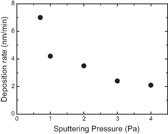
Figure 1. Variation of the deposition rate of TiO2 films as a function of the sputtering pressure.
Scanning electron microscope images of the TiO2 films prepared at different sputtering pressures are shown in Figure 2. Figure 2A shows the surface SEM images and Figure 2B shows the cross-sectional SEM images. From the Figure 2A, it can be seen that the rough surface has been obtained for all the films. Indeed, a rough surface is desirable for solar energy application because it allows the light that enters into the solar cells through the TCO layer to scatter efficiently so as to enhance absorption. It can also be seen that the structure is totally different for the films prepared at different sputtering pressures. For the film prepared at pressure of 0.7 Pa, only a close-packed compact structure can be observed. The surface view shows the various sizes of angular grains and no voids between the grains can be observed. For the films prepared at pressure higher than 1 Pa, the structure becomes different. Ball of yarn shaped grains and the voids between these grains are observed. The cross-sectional views show that these films have the nanorod structures. The TEM images shown that the surface of these nanorods is very rough (Meng et al., 2011a), which is favorable for the dye adsorption. From the surface view, it also can be seen that the voids between the grains become big as the sputtering pressure is increased. It means that the film prepared at high sputtering pressure has a more porous structure than film prepared at low sputtering pressure. The microstructure of thin films is related to the mobility of the adatoms during growth. Sputtered atoms from the target make their way on to the substrate through diffusion. At low sputtering pressure, sputtered atoms can reach the substrate without any collision, which means that they can reach the substrate with a relative high energy and result in a dense structure. At high sputtering pressure, the sputtered atoms will collide with the Ar ions or atoms before they reach the substrate and will lose their energy during the collisions. It means that they will reach the substrate with a relative low energy and form a porous structure. The results are agreed well with the structure zone model (Thornton, 1974).
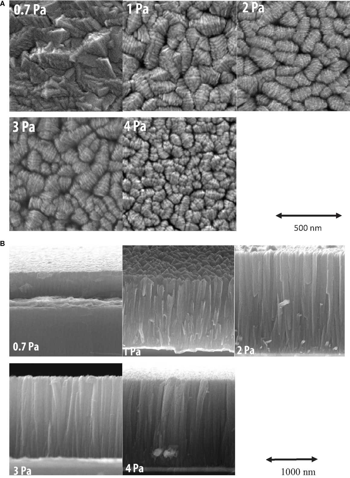
Figure 2. (A) The surface SEM images of TiO2 samples prepared at different sputtering pressures. (B) The cross-sectional SEM images of TiO2 samples prepared at different sputtering pressures.
Figure 3 shows the XRD patterns of TiO2 films deposited at different sputtering pressures. It can be seen that the film prepared at low sputtering pressure (0.7 Pa) has a preferred orientation along the [101] direction. The preferred orientation changes into the [110] direction as the sputtering pressure is higher than 1 Pa. All the peaks in the XRD patterns can be indexed as anatase phase of TiO2 and the diffraction data were in good agreement with PDF card 21–1272. No other phase of TiO2 has been observed. The [101] and the [220] peak intensities have been calculated by fitting the XRD patterns and the ratio of the I[220]/I[101] for the films prepared at different sputtering pressures has been presented in Figure 4. It can be seen that this ratio is increased from zero to the maximum value when the sputtering pressure is increased from 0.7 to 2 Pa and then decreases, as the sputtering pressure is increased further. From Figure 3 it can be seen that the [101] peak intensity does not show a very clear change when the sputtering pressure is higher than 1 Pa. It means that the film prepared at 2 Pa sputtering pressure has the strongest [220] diffraction peak intensity.
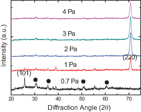
Figure 3. The X-ray diffraction patterns of TiO2 thin films deposited onto ITO substrates at different sputtering pressures. (• represents diffraction peaks from ITO substrate).
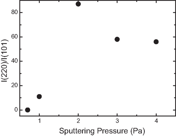
Figure 4. The XRD peak intensity ratio as a function of the sputtering pressure.
It is well known that the average surface energies of the [110], [001], [100], and [101] crystal planes of anatase TiO2 are 1.09, 0.90, 0.53, and 0.44 J/m2, respectively, which are related to the percentage of the fivefold coordinated titanium atoms on the specific planes (Lazzeri et al., 2002). Generally, anatase TiO2 single crystal is dominated by [101] planes, which are thermodynamically stable due to a low surface energy. However, for polycrystalline films, not only the surface energy but also the strain energy of grains formed in the films will influence the development of the texture. The effects of strain energy minimization are qualitatively similar to those of surface and interface energy minimization in that normal grain growth cannot occur until the subpopulation of grains favored by strain energy minimization has consumed all grains with other orientations (Thompson, 2000). The competition between surface energy and strain energy during film growth might contribute to the changes in texture of the grains as observed in Figure 3. For sufficiently thin films, surface and interface energy minimizing textures are favored but for the thicker films with higher elastic strains, strain energy minimizing textures are formed (Thompson, 2000). We have found that the [220] diffraction peak intensity increases with the film thickness and the results will be published elsewhere. It means that the [110] texture is dominated by strain energy minimization and the [101] texture is dominated by surface energy minimization in the growth process. At high sputtering pressure, the mobility of the adatoms in the substrate is low and might result in strain energy minimizing textures favorable during grain growth. At low sputtering pressure, the mobility of the adatoms in the substrate is high and might result in surface energy minimizing textures favorable during grain growth.
Figure 5 shows the Raman spectra of the TiO2 films prepared at different sputtering pressures. Five characteristic anatase Raman modes at 144, 199, 399, 516, and 640 cm-1, which are assigned to the Eg phononic mode represented by ν6, the Eg phononic mode represented by ν5, the B1g phononic mode represented by ν4, the B1g phononic mode plus the A1g phononic mode represented by ν3 + ν2, and the Eg phononic mode represented by ν1, respectively (Ohsaka et al., 1978; Karunagaran et al., 2003; Alhomoudi and Newaz, 2009), have been observed for all the samples. No other phases, such as rutile and brookite phases, have been observed, which are in agreement with XRD’s results as shown in Figure 3. It can be seen that the intensity of the Raman peaks decreases as the sputtering pressure increases. By fitting the Raman peak located at 144 cm−1, it has been found that the FWHM increases from 17.42 to 21.06 cm−1 as the sputtering pressure is increased from 0.7 to 4 Pa. Both the decrease of the peak intensity and the increase of the FWHM can be attributed to the deterioration of the crystallinity of the films. It means that the crystallinity of the TiO2 films prepared at high sputtering pressure has been deteriorated although they still have a preferred orientation along the [110] direction. This deterioration of the crystallinity of the film may result from the low adatoms mobility on the substrate at high sputtering pressure.
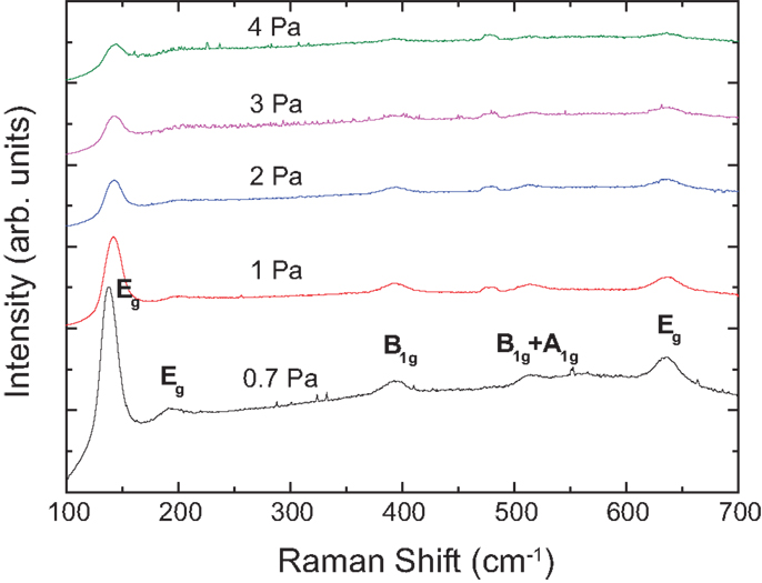
Figure 5. Raman spectra of TiO2 films deposited at different sputtering pressures. Peaks associated to anatase phase are indicated.
Figure 6 shows the photovoltaic performance of DSSCs based on the electrodes of TiO2 films prepared at different sputtering pressures. It can be seen that the DSSC based on the TiO2 film prepared at 0.7 Pa sputtering pressure has a very poor photocurrent density. The photocurrent has been improved for DSSCs using the TiO2 films prepared at the pressure higher than 1 Pa. And the highest photocurrent is reached for DSSC using the TiO2 film prepared at 2 Pa sputtering pressure. The performance of DSSCs and the characteristics are shown in Table 1 and plotted in Figure 7. The open-circuit voltage and the fill factor do not present a clear variation with the sputtering pressure. However, the short-circuit current and the conversion efficiency depend very much on the sputtering pressure. They show a similar variation with the sputtering pressure. It means, in these DSSCs, the photocurrent dominates the conversion efficiency. The highest conversion efficiency has been obtained for DSSC using TiO2 film prepared at 2 Pa sputtering pressure, which also shows the highest photocurrent density. Two key factors will affect the photocurrent density, photoelectron generation, and transportation. Photoelectron generation is related to the quantity of the dye adsorbed on the surface of TiO2 electrode. As it can be seen from the SEM images that the TiO2 film prepared at 0.7 Pa sputtering pressure has a very compact structure, which has a small surface area, and results in very small amount of dye molecules adsorbed on the surface and then a very low photocurrent density. When the sputtering pressure is higher than 1 Pa, the porous nanorods structure has been obtained. This structure has larger surface area than compact one and results in an increase of the number of the dye molecules adsorbed on the surface of the TiO2 and then a high photocurrent density. For clarifying qualitatively the dye adsorption, the transmittance of the TiO2 electrode before and after dye-sensitized have been measured as shown in Figure 8. The TiO2 electrode prepared at 0.7 Pa sputtering pressure can only adsorb a very small amount of dye molecules and the dye adsorption cannot be seen clearly by measuring the transmittance. So the transmittance spectra before and after dye-sensitized of this sample have not been shown in this figure. From Figure 8, it can be seen clearly that all the TiO2 electrodes have absorption around the 520 nm resulted from the dye molecules. It can also be seen that the absorption has a great increase when the sputtering pressure is increased from 1 to 2 Pa. When the sputtering pressure is increased further, the absorption shows a very small decrease. By fitting the transmittance of the TiO2 films prepared at different sputtering pressures, the refractive index of these films has been calculated and presented in Figure 9. The porosities of the films have been estimated using the refractive index of the films at 500 nm. The results are listed in Table 1. The porosity of the film increases from 1 to 24% when the sputtering pressure is increased from 0.7 to 1 Pa due to the change of the structure. The porosity increases gradually from 24 to 34% as the sputtering pressure is increased further from 1 to 4 Pa. Generally, the film with high porosity will absorb more dye molecules than the film with low porosity. It means that the absorption should always increase with the pressure. However, the absorption measuring results do not agree with this as shown in Figure 8. The porosity calculated with the refractive index may differ from the reality and the voids hided inside the film may not contribute for dye absorption. Both of them may cause this conflict result. From the SEM surface images, it can be seen that the voids between the nanorods are small for film prepared at 1 Pa sputtering pressure comparing to the films prepared at pressure higher than 2 Pa although all of them show nanorod structure. This may result in the low adsorption of the dye molecules and a low absorption as shown in Figure 8. When the pressure is higher than 2 Pa, the voids do not change clearly and result in a similar absorption. From Figure 7, it can be seen that the photocurrent density decreases with the pressure when it is higher than 2 Pa. The small decrease of the absorption with pressure as shown in Figure 8 may contribute this decrease of the photocurrent. However, it is suggested that the [220] crystallization also has contributions in it. The photoelectrons may have a large diffusion length along the [110] direction and result in an increase of the photocurrent density. From Figures 3 and 4, it can be seen that the [220] diffraction peak intensity decreases as the pressure is higher than 2 Pa and results in a low photocurrent density. It seems then that, in this matter, the higher porosity and the lower crystallinity that result from the increase of the sputtering pressure work in opposite tendencies; the best results being obtained for 2 Pa.
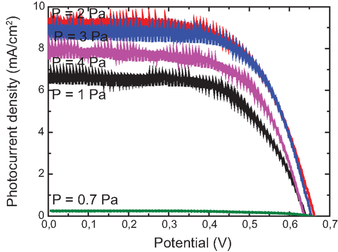
Figure 6. Current-potential characteristics of the TiO2 nanorods prepared at different sputtering pressures.
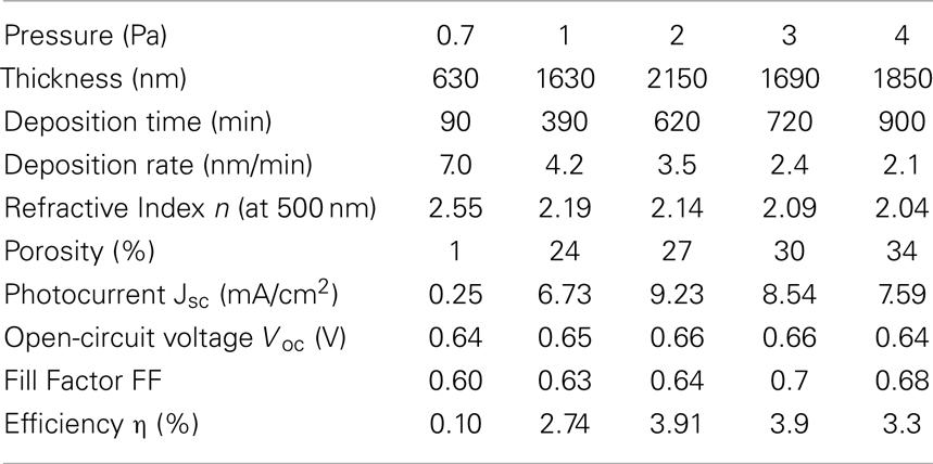
Table 1. Deposition conditions and photovoltaic performance of the DSSC based on TiO2 electrode prepared at different sputtering pressures.
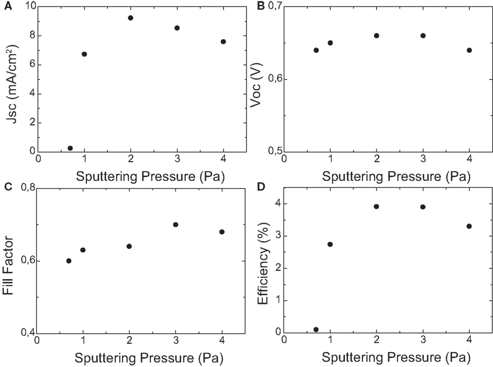
Figure 7. Variations of the short-circuit current density (A), the open-circuit voltage (B), the fill factor (C), and the conversion efficiency (D) as a function of the sputtering pressure.
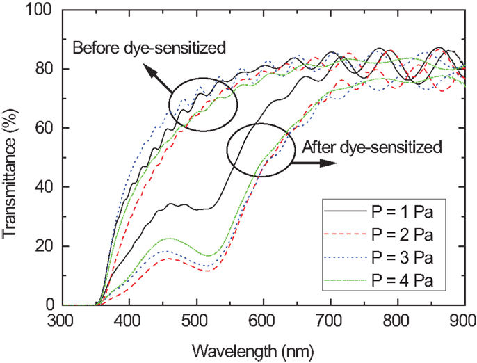
Figure 8. The transmittance of the TiO2 nanorods prepared at different sputtering pressures before and after dye-sensitized.
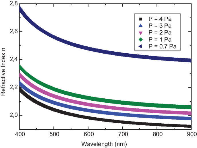
Figure 9. The refractive index of the TiO2 samples prepared at different sputtering pressures as a function of wavelength.
Conclusion
TiO2 films were prepared at different sputtering pressures by DC reactive magnetron sputtering. The [110] direction oriented nanorods structure were obtained for the films prepared at the pressure higher than 1 Pa. The [110] texture is dominated by strain energy minimization and the [101] texture is dominated by surface energy minimization in the growth process. The DSSCs assembled using these TiO2 films with nanorods structure show better conversion efficiency than those using TiO2 films with a compact structure. The [110] texture may favorite the charge transportation and the maximum conversion efficiency was achieved for DSSC assembled using TiO2 film with the strongest [110] texture.
Conflict of Interest Statement
The authors declare that the research was conducted in the absence of any commercial or financial relationships that could be construed as a potential conflict of interest.
Acknowledgments
This work is supported by the project PEst-OE/FIS/UI0068/2014 – CEFITEC.
References
Adachi, M., Murata, Y., Takao, J., Jiu, J., Sakamoto, M., and Wang, F. (2004). Highly efficient dye-sensitized solar cells with a titania thin-film electrode composed of a network structure of single-crystal-like TiO2 nanowires made by the “oriented attachment” mechanism. J. Am. Chem. Soc. 126, 14943–14949. doi: 10.1021/ja048068s
Alhomoudi, I. A., and Newaz, G. (2009). Residual stresses and Raman shift relation in anatase TiO2 thin film. Thin Solid Films 517, 4372–4378. doi:10.1016/j.tsf.2009.02.141
Burke, A., Ito, S., Snaith, H., Bach, U., Kwiatkowski, J., and Gratzel, M. (2008). The function of a TiO2 compact layer in dye-sensitized solar cells incorporating “Planar” organic dyes. Nano Lett. 8, 977–981. doi:10.1021/nl071588b
Gao, Y. F., Nagai, M., Seo, W. S., and Koumoto, K. (2007). Template-free self-assembly of a nanoporous TiO2 thin film. J. Am. Ceram. Soc. 90, 831–837. doi:10.1111/j.1551-2916.2007.01505.x
Gomez, M. M., Lu, J., Olsson, E., Hagfeldt, A., and Granqvist, C. G. (2000a). High efficiency dye-sensitized nanocrystalline solar cells based on sputter deposited Ti oxide films. Sol. Energy Mat. Sol. C 64, 385–392. doi:10.1016/S0927-0248(00)00231-2
Gomez, M. M., Lu, J., Solis, J. L., Olsson, E., Hagfeldt, A., and Granqvist, C. G. (2000b). Dye-sensitized nanocrystalline titanium-oxide-based solar cells prepared by sputtering: influence of the substrate temperature during deposition. J. Phys. Chem. B 104, 8712–8718. doi:10.1021/jp001566c
Gu, Z. Y., Gao, X. D., Li, X. M., Jiang, Z. W., and Huang, Y. D. (2014). Nanoporous TiO2 aerogel blocking layer with enhanced efficiency for dye-sensitized solar cells. J. Alloy Compd. 590, 33–40. doi:10.1016/j.jallcom.2013.12.097
He, B. L., Tang, Q. W., Luo, J. H., Li, Q. H., Chen, X. X., and Cai, H. Y. (2014). Rapid charge-transfer in polypyrrole-single wall carbon nanotube complex counter electrodes: improved photovoltaic performances of dye-sensitized solar cells. J. Power Sources 256, 170–177. doi:10.1016/j.jpowsour.2014.01.072
Hossain, M. F., Biswas, S., Takahashi, T., Kubota, Y., and Fujishima, A. (2008). Investigation of sputter-deposited TiO2 thin film for the fabrication of dye-sensitized solar cells. Thin Solid Films 516, 7149–7154. doi:10.1016/j.tsf.2007.12.022
Jiu, J., Isoda, S., Wang, F., and Adachi, M. (2006). Dye-sensitized solar cells based on a single-crystalline TiO2 nanorod film. J. Phys. Chem. B 110, 2087–2092. doi:10.1021/jp055824n
Kang, S. H., Kang, M. S., Kim, H. S., Kim, J. Y., Chung, Y. H., Smyri, W. H., et al. (2008). Columnar rutile TiO2 based dye-sensitized solar cells by radio-frequency magnetron sputtering. J. Power Sources 184, 331–335. doi:10.1016/j.jpowsour.2008.05.089
Karunagaran, B., Kumar, R. T. R., Kumar, V. S., Mangalaraj, D., Narayandass, S. K., and Rao, G. M. (2003). Structural characterization of DC magnetron-sputtered TiO2 thin films using XRD and Raman scattering studies. Mater. Sci. Semiconduct. Process. 6, 547–550. doi:10.1016/j.mssp.2003.05.012
Kuo, Y. Y., Lin, J. G., and Chien, C. H. (2012). Enhancing charge collection in dye-sensitized solar cells by trimming sidewall of the TiO2 nanotubes. J. Electrochem. Soc. 159, K46–K49. doi:10.1149/2.099202jes
Kwon, Y. S., Song, I. Y., Lim, J., Park, S. H., Siva, A., Park, Y. C., et al. (2012). Reduced charge recombination by the formation of an interlayer using a novel dendron coadsorbent in solid-state dye-sensitized solar cells. RSC Adv. 2, 3467–3472. doi:10.1039/c2ra01251k
Law, M., Greene, L. E., Johnson, J. C., Saykally, R., and Yang, P. D. (2005). Nanowire dye-sensitized solar cells. Nat. Mater. 4, 455–459. doi:10.1038/nmat1387
Lazzeri, M., Vittadini, A., and Selloni, A. (2002). Structure and energetics of stoichiometric TiO2 anatase surfaces (vol 63, art no 155409, 2001). Phys. Rev. B 65, 119901. doi:10.1103/PhysRevB.65.119901
Lee, B. H., Song, M. Y., Jang, S. Y., Jo, S. M., Kwak, S. Y., and Kim, D. Y. (2009). Charge transport characteristics of high efficiency dye-sensitized solar cells based on electrospun TiO2 nanorod photoelectrodes. J. Phys. Chem. C 113, 21453–21457. doi:10.1021/jp907855x
Liang, D. W., Tang, Q. W., Chu, L., Li, Q. H., He, B. L., Cai, H. Y., et al. (2013). Insights on the accumulation of charge carriers for enhanced electrical and photoelectric behaviors in conducting multilayer films. RSC Adv. 3, 25190–25196. doi:10.1039/c3ra44283g
Meng, L., Ma, A., Ying, P., Feng, Z., and Li, C. (2011a). Sputtered highly ordered TiO2 nanorod arrays and their applications as the electrode in dye-sensitized solar cells. J. Nanosci. Nanotechnol. 11, 929–934. doi:10.1166/jnn.2011.3084
Meng, L. J., Li, C., and dos Santos, M. P. (2011b). Effect of annealing temperature on TiO2 nanorod films prepared by DC reactive magnetron sputtering for dye-sensitized solar cells. J. Inorg. Organometal. Polym. Mater. 21, 770–776. doi:10.1007/s10904-011-9538-y
Meng, L. J., and Li, C. (2011). Blocking layer effect on dye-sensitized solar cells assembled with TiO2 nanorods prepared by DC reactive magnetron sputtering. Nanosci. Nanotechnol. Lett. 3, 181–185. doi:10.1166/nnl.2011.1143
Meng, L. J., Li, C., and dos Santos, M. P. (2013). Structural modification of TiO2 nanorod films with an influence on the photovoltaic efficiency of a dye-sensitized solar cell (DSSC). J. Inorg. Organometal. Polym. Mater. 23, 787–792. doi:10.1007/s10904-013-9842-9
Meng, L. J., Ren, T., and Li, C. (2010). The control of the diameter of the nanorods prepared by DC reactive magnetron sputtering and the applications for DSSC. Appl. Surf. Sci. 256, 3676–3682. doi:10.1016/j.apsusc.2009.12.169
Ngamsinlapasathian, S., Sakulkhaemaruethai, S., Pavasupree, S., Kitiyanan, A., Sreethawong, T., Suzuki, Y., et al. (2004). Highly efficient dye-sensitized solar cell using nanocrystalline titania containing nanotube structure. J. Photochem. Photobiol. A 164, 145–151. doi:10.1016/j.jphotochem.2003.11.016
Ohsaka, T., Izumi, F., and Fujiki, Y. (1978). Raman-spectrum of anatase, TiO2. J. Raman Spectrosc. 7, 321–324. doi:10.1002/jrs.1250070606
O’Regan, B., and Gratzel, M. (1991). A low-cost, high-efficiency solar-cell based on dye-sensitized colloidal TiO2 Films. Nature 353, 737–740. doi:10.1038/353737a0
Park, J. T., Chi, W. S., Jeon, H., and Kim, J. H. (2014). Improved electron transfer and plasmonic effect in dye-sensitized solar cells with bi-functional Nb-doped TiO2/Ag ternary nanostructures. Nanoscale 6, 2718–2729. doi:10.1039/c3nr05652j
Ren, J. B., Que, W. X., Yin, X. T., He, Y. C., and Javed, H. M. A. (2014). Novel fabrication of TiO2/ZnO nanotube array heterojunction for dye-sensitized solar cells. RSC Adv. 4, 7454–7460. doi:10.1039/c3ra45741a
Sabba, D., Agarwala, S., Pramana, S. S., and Mhaisalkar, S. (2014). A maskless synthesis of TiO2-nanofiber-based hierarchical structures for solid-state dye-sensitized solar cells with improved performance. Nanoscale Res. Lett. 9, 14. doi:10.1186/1556-276X-9-14
Shao, F., Sun, J., Gao, L., Chen, J. Z., and Yang, S. W. (2014). Electrophoretic deposition of TiO2 nanorods for low-temperature dye-sensitized solar cells. RSC Adv. 4, 7805–7810. doi:10.1039/c3ra47286h
Sung, Y. M., and Kim, H. J. (2007). Sputter deposition and surface treatment of TiO2 films for dye-sensitized solar cells using reactive RF plasma. Thin Solid Films 515, 4996–4999. doi:10.1016/j.tsf.2006.10.079
Thavasi, V., Renugopalakrishnan, V., Jose, R., and Ramakrishna, S. (2009). Controlled electron injection and transport at materials interfaces in dye sensitized solar cells. Mat. Sci. Eng. R 63, 81–99. doi:10.1016/j.mser.2008.09.001
Thompson, C. V. (2000). Structure evolution during processing of polycrystalline films. Annu. Rev. Mater. Sci. 30, 159–190. doi:10.1038/srep03635
Thornton, J. A. (1974). Influence of apparatus geometry and deposition conditions on structure and topography of thick sputtered coatings. J. Vac. Sci. Technol. 11, 666–670. doi:10.1116/1.1312732
Waita, S. M., Aduda, B. O., Mwabora, J. M., Granqvist, C. G., Lindquist, S. E., Niklasson, G. A., et al. (2007). Electron transport and recombination in dye sensitized solar cells fabricated from obliquely sputter deposited and thermally annealed TiO2 films. J. Electroanal. Chem. 605, 151–156. doi:10.1016/j.jelechem.2007.04.001
Wang, H. X., Liu, M. N., Zhang, M., Wang, P., Miura, H., Cheng, Y., et al. (2011). Kinetics of electron recombination of dye-sensitized solar cells based on TiO2 nanorod arrays sensitized with different dyes. Phys. Chem. Chem. Phys. 13, 17359–17366. doi:10.1039/c1cp22482d
Wang, H. X., and Peter, L. M. (2012). Influence of electrolyte cations on electron transport and electron transfer in dye-sensitized solar cells. J. Phys. Chem. C 116, 10468–10475. doi:10.1021/jp211807w
Wu, M. X., Lin, X., Wang, T. H., Qiu, J. S., and Ma, T. L. (2011). Low-cost dye-sensitized solar cell based on nine kinds of carbon counter electrodes. Energy Environ. Sci. 4, 2308–2315. doi:10.1039/c1ee01059j
Wu, M. X., Lin, X., Wang, Y. D., Wang, L., Guo, W., Qu, D. D., et al. (2012). Economical Pt-free catalysts for counter electrodes of dye-sensitized solar cells. J. Am. Chem. Soc. 134, 3419–3428. doi:10.1021/ja209657v
Zhang, X. B., Tian, H. M., Wang, X. Y., Xue, G. G., Tian, Z. P., Zhang, J. Y., et al. (2013). The different electron transport of two nanotubes incorporated in working electrode of dye-sensitized solar cells. J. Alloy Compd. 578, 309–313. doi:10.1016/j.jallcom.2013.06.041
Zhang, X. B., Tian, H. M., Wang, X. Y., Xue, G. G., Tian, Z. P., Zhang, J. Y., et al. (2013a). The role of oxygen vacancy-Ti3+ states on TiO2 nanotubes’ surface in dye-sensitized solar cells. Mater. Lett. 100, 51–53. doi:10.1016/j.matlet.2013.02.116
Zhang, X. H., Ogawa, J., Sunahara, K., Cui, Y., Uemura, Y., Miyasaka, T., et al. (2013b). Alternation of charge injection and recombination in dye-sensitized solar cells by the addition of nonconjugated bridge to organic dyes. J. Phys. Chem. C 117, 2024–2031. doi:10.1021/jp310425z
Zhao, X. G., Jin, E. M., and Gu, H. B. (2013). Increased charge transfer of PVDF-HFP based electrolyte by addition of graphite nanofiber and its application in dye-sensitized solar cells. Appl. Surf. Sci. 287, 8–12. doi:10.1016/j.apsusc.2013.09.017
Keywords: TiO2, DSSC, nanorod, structural property, sputtering
Citation: Meng L, Chen H, Li C and dos Santos MP (2014) Growth of the [110] oriented TiO2 nanorods on ITO substrates by sputtering technique for dye-sensitized solar cells. Front. Mater. 1:14. doi: 10.3389/fmats.2014.00014
Received: 25 July 2014; Paper pending published: 06 August 2014;
Accepted: 16 August 2014; Published online: 05 September 2014.
Edited by:
Weijie Song, Chinese Academy of Sciences, ChinaCopyright: © 2014 Meng, Chen, Li and dos Santos. This is an open-access article distributed under the terms of the Creative Commons Attribution License (CC BY). The use, distribution or reproduction in other forums is permitted, provided the original author(s) or licensor are credited and that the original publication in this journal is cited, in accordance with accepted academic practice. No use, distribution or reproduction is permitted which does not comply with these terms.
*Correspondence: Lijian Meng, Rua Dr. António Bernardino de Almeida 431, Porto, Portugal e-mail: ljm@isep.ipp.pt