Optical properties of germanium nanoparticles synthesized by pulsed laser ablation in acetone
 Saikiran Vadavalli1
  Sreeramulu Valligatla1,2,3 Bharati Neelamraju1 Mudasir H. Dar1 Alessandro Chiasera2 Maurizio Ferrari2
  Narayana Rao Desai1*
- 1School of Physics, University of Hyderabad, Hyderabad, India
- 2Dipartimento di Fisica, Università di Trento, Trento, Italy
- 3CNR-IFN, CSMFO Lab, Trento, Italy
HIGHLIGHTS
• We have successfully synthesized Ge NPs in acetone using pulsed laser ablation.
• The average size of NPs is found to decrease with the increase in laser pulse energy.
• The NP number density increases with the increase in pulse energy of the ablation.
• Size dependent blue luminescence has been observed from the synthesized Ge NPs.
• The shift in the Raman peak position has been interpreted as due to the quantum confinement and the strain in the NPs.
• The measured NP sizes from the micro-Raman studies suggest that the phonon quantum confinement model is in good agreement with the TEM measurements of Ge NPs sizes.
Germanium (Ge) nanoparticles (NPs) are synthesized by means of pulsed laser ablation of bulk germanium target immersed in acetone with ns laser pulses at different pulse energies. The fabricated NPs are characterized by employing different techniques such as UV-Visible absorption spectroscopy, photoluminescence, micro-Raman spectroscopy, transmission electron microscopy (TEM) and field emission scanning electron microscopy (FESEM). The mean size of the Ge NPs is found to vary from few nm to 40 nm with the increase in laser pulse energy. Shift in the position of the absorption spectra is observed and also the photoluminescence peak shift is observed due to quantum confinement effects. High resolution TEM combined with micro-Raman spectroscopy confirms the crystalline nature of the generated germanium nanoparticles. The formation of various sizes of germanium NPs at different laser pulse energies is evident from the asymmetry in the Raman spectra and the shift in its peak position toward the lower wavenumber side. The FESEM micrographs confirm the formation of germanium micro/nanostructures at the laser ablated position of the bulk germanium. In particular, the measured NP sizes from the micro-Raman phonon quantum confinement model are found in good agreement with TEM measurements of Ge NPs.
Introduction
Semiconductor nanoparticles (NPs) or quantum dots are very attractive and interesting area of current research. There are many significant developments made in the synthesis, characterization and application oriented development of these fascinating materials [1, 2]. The effect of quantum confinement in the semiconductor NPs on the optical properties of semiconductors is mainly responsible for the growing interest as an attractive area of research. The interest in the basic semiconductor NPs of silicon and germanium is high as they show highly good luminescence properties at the nanoscale whereas there is no emission from them in their bulk form [3]. Further studies on Si and Ge—NPs are very interesting because of their size dependent optical properties which can lead to many technologically important applications such as optical light emitting devices [4], integrated flash memory devices [5] solar cell technology [6] and in biomedicine [7]. Bulk crystalline Si and Ge are also leading materials in microelectronics industry because of their semiconducting properties [8, 9]. In the fastest growing field of the nanoscience and nanotechnology, the integration of optoelectronic devices with the microelectronics which show efficient optical properties along with their integration in electronic technology is needed. Si and Ge nanocrystals (NCs) are considered to be ideal candidates for optoelectronic applications because they show emission in the visible region [10, 11]. The added advantage is that Si and Ge are non-toxic and environmentally friendly green materials [12], so that they can replace toxic semiconducting materials in the optoelectronic research of optical lighting and display applications. The efficient luminescence properties at room temperature are due to their strong quantum confinement effects in the nanoscale [13]. Out of these two, Ge (24 nm) has larger Bohr exciton radius in comparison with the Si (6 nm), and also by considering the effective masses and energy differences between the indirect gaps, the Ge NCs have better technological advantages over Si NCs [14]. Mostly in all the preparation processes, the Ge nanocrystals are embedded in a dielectric (SiO2) matrix. All these methods include mainly the deposition of thin films by physical/chemical method and then followed by high temperature annealing for the formation of nanoparticles. Co-sputtering [15], sol-gel synthesis [16], ion implantation [17], etc. are few more popular methods to mention out of the many available techniques. Formation of Ge layer containing Ge NCs formed by electrochemical etching was reported very recently [18, 19]. All these techniques produce broad distributions of particle sizes and needs high end vacuum based deposition systems along with high temperature furnaces. Though there have been few reports available on Ge NPs synthesis through sol gel route [20, 21], in general the solution based sol-gel synthesis of Ge NPs is more difficult because of the lack of knowledge of highly crystalline monodisperse samples for initial starting precursors [22]. Synthesis of germanium nanoparticles (NPs) in a simple, cheap and green procedure with sizes tuned to desired optical and electronic properties can be a multifaceted task. Optimization of new methods for the preparation of nanostructures using a range of available techniques has therefore become an important area of materials research. One relatively simple, inexpensive and green synthesis method for synthesizing nanoparticles of desired sizes at room temperatures is pulsed laser ablation in liquids (PLAL) from bulk targets [23–25]. Lasers have been used for materials processing because of their high energy. Laser ablation uses the energy of short laser pulses to remove some of the material from its source/bulk target. High intensity pulses on a material under controlled pressure and temperature conditions can lead to the generation of nanoparticles of the material in the solution. Laser ablation in liquids has the advantage that it can be done at room temperatures and control on the properties of the nanoparticles can be achieved by varying the liquid properties and laser ablation parameters. This technique is therefore considered effective for the synthesis of colloidal solutions of nanoparticles. Overall it is a fast, cheap and clean (green) method of preparation of a variety of nanoparticles.
Among the two, Si and Ge NPs by pulsed laser ablation in liquids more efforts and research has been carried out on Si in comparison with that of Ge [26–29]. The literature on the synthesis of Ge NPs [30, 31] by PLAL is limited and so the understanding of Ge NPs formation by PLAL and the tuning of optical properties by varying different input parameters is very much needed. In this paper we focus on the synthesis of germanium NPs by pulsed laser ablation (PLA) in acetone and the optical and structural characterization of thus synthesized NPs using different methods such as Raman spectroscopy, transmission electron microscopy (TEM), optical absorption, X-Ray diffraction (XRD), photoluminescence (PL) etc. Here we have mainly studied the laser pulse energy dependence on the average size of the Ge NPs synthesized by pulsed laser ablation with nanosecond laser pulses. The blue photoluminescence and the size dependent shift in the micro-Raman spectra have been discussed in detail. The results have been understood based on the phonon confinement model.
Experimental Details
NP Synthesis
Commercially available p-type Ge (100) wafer with 0–30 ohm-cm resistivity was used for the fabrication of Ge NPs. Germanium target was ultrasonically cleaned with distilled water and then with acetone for 20 min before the ablation process. Q-switched Nd: YAG pulsed laser delivering 10 Hz repetition rate pulses with 6 ns pulse width at 1064 nm fundamental wavelength was used for the laser ablation of Ge wafer. The cleaned germanium wafer was placed at the bottom of the beaker and filled with 10 ml of acetone. After keeping the substrates perfectly parallel to the optical bench, the laser pulses were allowed to focus on the substrates with a plano-convex lens (focal length f = 10 cm) for different times. Different pulse energies of 60, 40, and 20 mJ were used for the generation of germanium NPs to see the effect of pulse energy on the formation of Ge NPs. During the laser ablation, the target was moved using a rotation system to achieve more and uniform irradiation of germanium surface. The laser was focused normally on the target for ablation. After 30 min irradiation, the solution became light brown in color which indicates the formation of Ge NPs. The ablated solution was then used for all the characterizations. To confirm the presence of Ge NPs the same solution was ablated without keeping Ge wafer for the same duration of time at the same energy. Figure 1 shows the schematic diagram of a typical experimental setup for pulsed laser ablation in liquids (PLAL). The setup basically consists of a pulsed laser, beam delivery optics, and a container to hold the target and liquid (acetone in the present case). The setup may be modified to control the ablation process, but the common features still exist, that is, a laser beam is focused onto a target immersed in liquid, and the ablated materials are dispersed into the liquid.
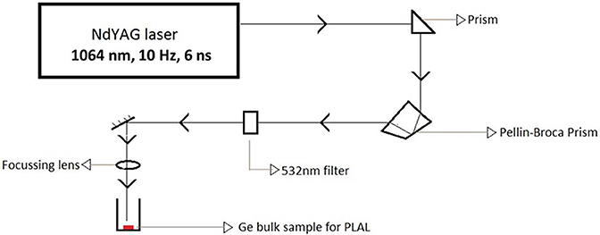
Figure 1. Schematic of the experimental setup of pulsed laser ablation in liquids.
NP Characterization
The Raman measurements were carried out with HR 800 Horiba Jobin Yvon model, at room temperature using 632 nm line of a He-Ne laser as the excitation wavelength. The Raman scattering measurements were carried out (1) on the drop casted NPs solutions on a glass plate (cover slip) (2) on the ablated position of the Ge wafer and (3) unablated Ge wafer. Raman spectrum gives detailed information on the vibrational energies of the different sizes of Ge NPs and it is a non-destructive method. The Raman spectra were recorded in the backscattering geometry at room temperature. Calibration was performed with a silicon wafer by utilizing the first order phonon band of Si at 520 cm−1 before and after recording. The laser light was focused on the NPs sample with a 10 × objective lens and the backscattered light was collected into the LabRam spectrometer equipped with a grating having 1800 grooves/mm. To avoid the heating of the samples with the laser beam we have used low powers of the excited laser (≤2 mW). The surface morphology of the laser ablated wafer was studied using field emission scanning electron microscopy (FESEM—Carl Zeiss, FEG, Ultra 55) with operating voltage at 5 kV. The images and the structural characteristics of Ge NPs have been studied by using advanced TEM (Tecnai 20 G2 STwin) with an electron-accelerating voltage of 200 kV. The Ge NPs solution was drop casted on to carbon coated copper TEM grids and glass substrates for TEM and FESEM measurements, respectively. The photo absorption and photoluminescence measurements were carried out on the Ge NPs solutions by taking them in well cleaned 10 ml quartz cuvettes. The photo absorption measurements were carried out using double beam UV-Visible spectrophotometer (Jasco V-657) ranging from 200 to 1000 nm. The fluorescence measurements were performed in the visible region using Fluorolog spectrometer (Horiba-Jobin, PL-Fluorolog, Xenon lamp, 450 W, Excitation wavelength: 355 nm, Resolution: 0.3 nm) to observe the luminescence properties of Ge NPs solution. XRD measurements were carried out in glancing angle incidence mode with an incidence angle of 1° using a Cu Kα source (1.5406 Å) on the glass plate where the Ge NPs solution was drop casted. Structural characterization and elemental composition of the Ge NPs were observed by selective area electron diffraction (SAED) and energy dispersive X-ray spectroscopy analysis (EDS) both of which are associated with TEM.
Results and Discussion
Raman Results
Micro-Raman spectroscopy measurements have been performed on all the different types of samples synthesized in acetone at different energies and also on the ablated Ge wafers separately. Raman spectra of unablated bulk crystalline Ge (pure) and laser ablated Ge at different laser pulse energies are shown in Figure 2A. The Raman peak due to Ge-Ge vibrational modes of the bulk crystalline Ge wafer falls at 300 cm−1 (with FWHM of ~3 cm−1) which is symmetrical at the peak position. The Raman spectrum of the ablated region of the Ge wafer contains a second peak, which is attributed to the NP adherence to the Ge wafer. The second peak shows a shift in its vibrational frequency that increases with the increase of laser pulse energy. The shift is more at higher energies when compared with that at lower energies. We also recorded the Raman spectra of only Ge NPs by evaporating NP solution on a cover glass slide and the observed spectra are shown in Figure 2B. When we compare the two spectra, Figures 2A,B, we observe that the 300 cm−1 peak for the NPs on glass slide show a shift of around 4 cm−1 (maximum), while the NPs on the Ge wafer shows a side peak shift of around 9 cm−1 (maximum). This is a consequence of decrease in the average size of Ge NPs [32, 33]. We did not observe any shift in the main peak at 300 cm−1 in Figure 2A which is that of the Ge-Ge vibrational band of the wafer alone. However, we can clearly see an asymmetry in the peak toward lower wavenumber side along with the second peak that has the contribution of the NPs' adherence to the Ge wafer [the two peaks can be clearly distinguished in the deconvoluted Raman spectra shown in Figure 2D].
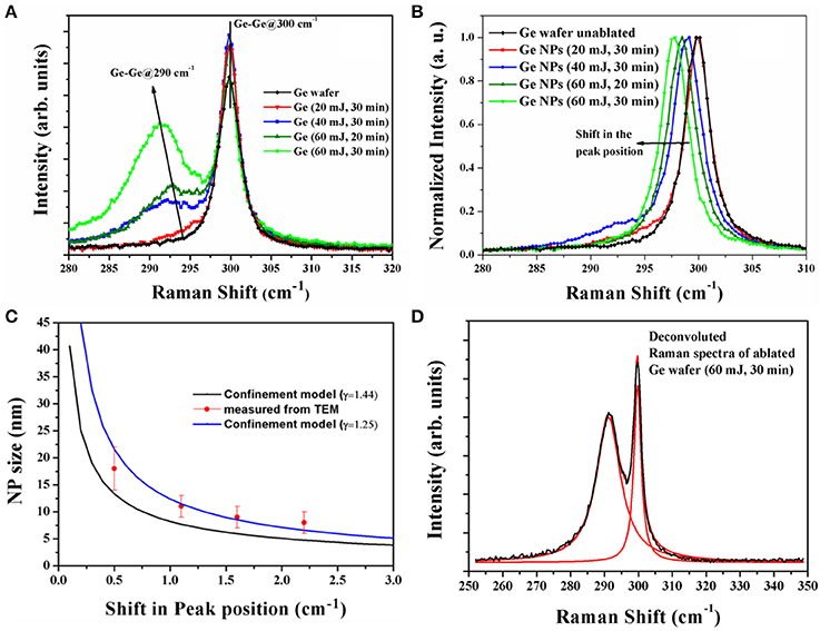
Figure 2. Micro Raman spectra of (A) laser ablated Ge wafer at different laser pulse energies, (B) different energy synthesized Ge NPs in acetone drop casted on glass slide, (C) variation of NP size with shift in the Raman peak position according to equation 2 (for different γ-values) points are the Ge NP sizes calculated from TEM (given in Table 1) along with the standard deviations and (D) deconvoluted Raman spectra of ablated Ge.
The observed results are interpreted as due to the strains of various extents and are discussed below. For the NPs on the glass slide, larger the size of the NPs the smaller the shift observed, which is understandable as the surface to volume ratio decreases for the larger sized particles and hence the lower strain effects are expected for larger sized particles. So the shift observed can be attributed to the quantum confinement, which is related to sizes [34]. However, for the particles that adhere to the Ge wafer immediately after the ablation, we expect an additional strain at the interface of the bulk Ge and the NPs. Both the spectra (Figures 2A,B) agree and also show consistency. Figure 2B doesn't show the side peak that is observed in Figure 2A, which is attributed as to the Ge-Ge vibrational modes of the NPs and the Ge surface atoms. This shift in the peak position and the increase in FWHM indicate that a size reduction of the NPs due to the pulse energy of the laser. The Raman peak position values for different laser pulse energy synthesized Ge NPs in the solution have been given in the Table 1. The broadening and shift toward the lower wavenumber side can be related to the nanoparticle size using the phonon confinement model which can be given by the equation for the first order Raman spectrum as [35, 36]:
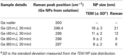
Table 1. Comparison of Ge Nanoparticle sizes of different samples measured from TEM and Raman spectroscopy (phonon confinement model).
Where “q” is expressed in terms of 2π /a, and a is the lattice constant of Ge (0.5658 nm), d is the size of the Ge nanoparticle. Γ0 (= 3.2 cm−1) is the natural line width of the transverse optical (TO) phonon in crystalline bulk Ge at room temperature and ω(q) is the TO phonon dispersion frequency relation at q. By using the above equation along with the dispersion relation and considering the downshift of the Raman peak and the peak broadening with respect to the bulk Ge, the average nanoparticle size can be estimated. The equation that relate the peak shift with the NP size can be given after simplification as [37]:
where the values are A and γ are constants and a is the lattice parameter of Ge (0.5658 nm). The measured peak shifts in the Raman peak are compared with this formula and estimated the Ge NP size. Figure 2C shows a fit of experimentally observed data with the Equation (2) as based on the quantum effects. We fitted the data of the NPs suspended in the solution with the equation 2 using the constants A and γ as 47.41 and 1.25 respectively. The value of γ slightly differs from the earlier reported value 1.44 [37]. This variation could be due to the difference in the synthesis procedures followed. The quantum confinement model is applied to the NPs on a glass slide (peak at 300 cm−1), and the same cannot be applied to the side peak of NPs adhered to the Ge wafer as there are additional strains coming at the interface of the particle and the bulk Ge. It is observed that the NP size values measured here are in close agreement with the NP sizes obtained from TEM measurements as can be seen from the Figure 2C. No peak is observed around 440 cm−1 which indicates that GeO2 phase has not been formed in the NPs [38]. Only major peak corresponding to Ge-Ge optical phonon mode at 300 cm−1 with lower shift along with the asymmetry is observed in the Raman spectra. Hence it is concluded that the size dependent Ge NPs have formed due to laser ablation of Ge wafer in acetone. A broad peak centered at 270 cm−1 is also not observed so there is no formation of amorphous Ge [39]. Thus, pure Ge NPs have been observed and with the increase of laser ablation energy the NP size decreases and the number density of the NPs formed increases.
TEM Results
Structural characterization of the synthesized Ge NPs was carried out using TEM imaging to understand the dispersion, average size of the Ge NPs in the solvent and the density of formed NPs. Figure 3 show the TEM images of Ge NPs formed in acetone. We have observed that the Ge nanoparticles are well dispersed in acetone. The NPs formed in acetone at different energies of the incident laser pulse are shown in Figure 3. Figure 3C shows the Ge NPs formed at high energy ablation but ablated for 20 min only whereas Figures 3A,B,D corresponds to the Ge NPs synthesized in acetone with different energies for 30 min duration of the ablation. With the increase in laser pulse energy we have observed that the Ge NPs concentration increased and the average size was observed to be decreased as seen from the Figure 3. At a fixed energy with the increase of duration of ablation we have observed only a slight change in the NP size. The image J software was used to analyze the average size of nanoparticles and their distribution. Figures 4A–C gives the size distribution histograms of the Ge NPs synthesized at different conditions. Figure 4D shows the elemental composition of the Ge NPs recorded by using energy dispersive X-ray spectroscopy (EDS) associated with TEM, which confirms the Ge NPs composition. We noticed a decrease in the average size of the NPs with the increase in the laser pulse energy used for ablation. The values are summarized and given in the Table 1. We have observed that the Ge NPs formed in different ablation conditions are lesser than the Bohr radius value of Ge hence efficient quantum confinement is possible with these formed nanoparticles.
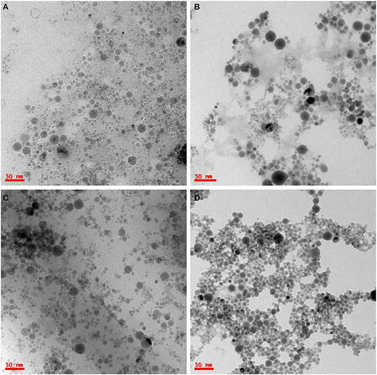
Figure 3. TEM images of Ge NPs obtained by laser ablation of Ge wafer in acetone at laser pulse energy of (A) 20 mJ (30 min duration), (B) 40 mJ (30 min duration), (C) 60 mJ (20 min duration), and (D) 60 mJ (30 min duration).
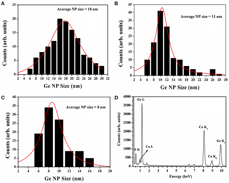
Figure 4. (A–C) are the size distribution histograms of 20 mJ (30 min duration), 40 mJ (30 min duration), and 60 mJ (30 min duration) samples respectively. (D) Shows the elemental composition from the Ge NPs recorded using EDS associated with TEM.
The SAED pattern recorded from the Ge NPs is shown in the Figure 5C along with the high resolution TEM image of the single Ge NPs (Figures 5A,B). The diffraction patterns have been assigned to the Ge (111), (220), and (311) diffraction planes respectively by measuring the d-spacing value and it is matching with the respective JCPDS file (Card No # 04–0545). It was observed that the Ge NPs formed in the acetone are highly crystalline. The lattice planes are matched with the diamond structure of Ge. The lattice constant calculated from these spots is ~0.565 nm which is in consistent with the Ge lattice constant. The high resolution TEM image also shows the highly oriented planes of the crystalline Ge with d-spacing 0.32 nm in the (111) direction.
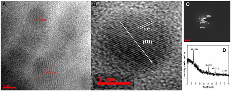
Figure 5. (A) High resolution TEM image of Ge nanoparticles and (B) HRTEM image of single Ge NP, (C) the corresponding SAED pattern of Ge NPs and (D) XRD pattern of the drop casted Ge NPs solution (acetone) on the glass slide.
The solution containing Ge NPs was drop casted on the glass plate and dried at room temperature for few hours. The dried glass slide was used to record the XRD pattern and the XRD pattern of the Ge NPs is shown in Figure 5D. It shows that the Ge NPs formed in the solution are crystalline with diamond structure. All the Ge nanoparticle peaks with (111), (220), and (311) orientations have been noticed at their respective 2θ positions. We have calculated micro strain values using Williamson-hall method [40] from the XRD pattern of these Ge NPs and we have found that the strain value is around 3 × 10⁻⁴. So the shift in the Raman peak is mainly due to the quantum confinement related to NP size where the particles of different sizes also experience different strains.
FESEM Results
FESEM has been used to study the surface morphology and the formation of micro/nano structures upon laser ablation in acetone. We have recorded FESEM on the laser ablated Ge wafer as well as the NPs solution drop casted on the glass slide. FESEM images further confirmed Ge NP formation and the particle distribution changes with input laser pulse energy. Figures 6A–C show the Ge nanoparticle formation at laser pulse energies of 20, 40, and 60 mJ from the bulk Ge wafer for 30 min duration of the ablation. Similar to TEM, we conclude the number of particles (particle density) formed increases with increase in laser pulse energy. From the images it was clear that the Ge gets modified in micro and nano regions at the ablated position of the wafer. So there are modified micro regions in which nano sized Ge particles formed on the ablated wafer. Figure 6D shows the FESEM image of the drop casted solution on the glass slide. This clearly confirms the formation of well dispersed Ge NPs in the solution, which was earlier confirmed from Raman and TEM measurements.
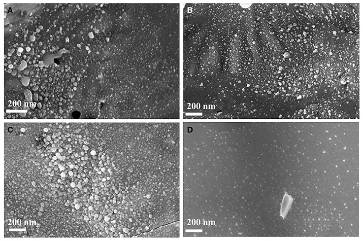
Figure 6. FESEM images of laser ablated Ge wafer in acetone at different laser pulse energies of (A) 20 mJ, (B) 40 mJ, (C) 60 mJ, and (D) FESEM image of drop casted Ge NPs.
Absorption and PL Results
The photo physical properties have been investigated by using optical absorption (UV-Vis) and photoluminescence emission spectroscopies. The photo absorption spectra of the Ge NPs synthesized at different laser pulse energies in acetone are shown in Figure 7. From the absorption spectra it is clear that the spectra exhibit a peak centered at around 335 nm with its tail extending to the red region (600 nm) and the peak position shifts with the laser pulse energy for different samples. A small blue shift (decrease in wavelength) in absorption wavelength was noticed with the increase of laser pulse energy which signifies a decrease in average size of Ge NPs. The Bohr radius of Ge NP is around 24 nm, and the peak at 335 nm is attributed to quantum effects of the NPs below the Bohr radius. Though the NPs size distribution from TEM appears reasonably narrow which should have made the peak to be distinct, a long tail forms on the lower energy side due to the formation of defects during laser irradiation. The NPs distributed in the solution thus show a wide absorption band. Similar kind of absorption was reported for the Ge NPs formed in water [22] but we are reporting the formation of Ge NPs in acetone at different energies for the first time.
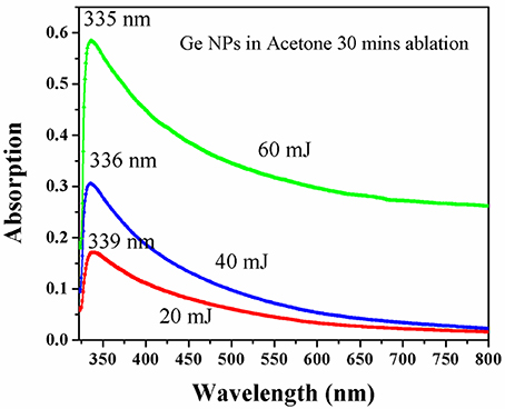
Figure 7. UV Visible absorption spectra of the various laser pulse energy synthesized Ge NPs in acetone.
On the other hand the Figure 8 shows the PL spectra of the Ge NP colloidal solutions prepared at different laser pulse energies. The PL spectra look broad ranging from 380 to 500 nm with peak positions at different wavelengths for different laser energy of the ablation. The difference in PL peak wavelengths of Ge NPs synthesized with different energies at a given excitation wavelength of 355 nm can be directly visible from the spectra. The PL spectra indicate the emission in the blue region and shows that the Ge NPs are blue luminescent in nature. This observed emission is attributed to the interband emission from Ge NPs than due to the defect states. The defect states continuously extend till 2.1 eV (600 nm) and therefore do not yield any emission in the visible region and decay through non-radiative processes. Thus, the observed blue emission is primarily due to the interband transition effects, where the relevant states are, a quantized state at around 335 nm and the ground state. There are several reports available on the blue emission of Ge NPs synthesized by different methods which say that the reason for the emission is purely due to the formation of size dependent Ge NPs. Here we are reporting the Ge NPs synthesis by laser ablation of Ge in acetone. Previously Ghosh et al. [13] have reported the green luminescent Ge NPs by laser ablation of Ge in 1-octene. Our studies are in acetone and the PL peak position is found to shift slightly toward the lower wavelengths with the increase in laser pulse energy which is a consequence of the decrease of Ge NP size. The colloidal Ge NPs prepared at lower and medium energy ablation show a broader emission with double/multiple peak positions (423, 442, 483 nm), whereas the Ge NPs prepared at higher energy ablation show a single peak emission (mostly at 418 nm). The reason for such observation is the size distribution of Ge NPs formed in the higher energy ablation is sharper than the size distribution of Ge NPs formed in the lower and medium energy ablation. The number density of Ge NPs is different in different samples and in the high energy ablation case the sample has more number of NPs. There are several earlier reports which present the PL emission of Ge NPs in the blue-green spectral region [11, 41–43] and from those reports it was observed that different synthesis methods of Ge NPs yields different emission. So here we may expect the change in emission wavelength depending on the solvent because Ghosh et al. [13] have shown the green emission from Ge NPs synthesized by laser ablation in 1-octene. Hence further studies with different solvents on the optical emission properties of the Ge NPs and their structural studies are planned.
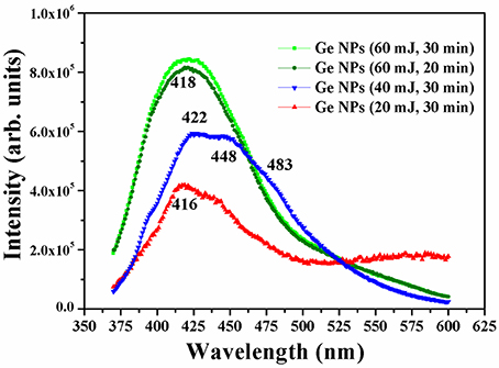
Figure 8. Photoluminescence spectra of Ge NPs colloids prepared at different laser input energies.
Conclusions
We have successfully synthesized the Ge nanoparticles by a versatile and green synthesis method pulsed laser ablation in liquids (PLAL), for the present case in acetone. Ge nanoparticle formation on the ablated wafer and as well in the solution was also achieved. The formation of NPs was confirmed from various characterization methods such as Raman spectroscopy, TEM, FESEM, optical absorption, XRD and PL. We have observed that the average size of the NPs decreases with the increase in the laser energy during ablation process. The NP number density in the solution was also observed to be more in the high energy ablated case i.e., the more no of NPs are formed at high energy ablation in the liquid. The particles have been formed without agglomeration in acetone and with good dispersion and size distribution as evident from TEM. Size dependent Raman shifts were observed from the analysis of the Raman spectra. Finally the measured NP sizes from micro-Raman phonon quantum confinement model are found in good agreement with TEM measurements of Ge NPs.
Conflict of Interest Statement
The authors declare that the research was conducted in the absence of any commercial or financial relationships that could be construed as a potential conflict of interest.
Acknowledgments
This research has been performed in the framework of the India-Trento Program for Advanced Research ITPAR Phase III research Project. VS acknowledge the post-doctoral fellowship and DNR acknowledges financial support received from Department of Science and Technology (DST) India through the Project No. SR/S2/LOP-17/1012.
References
1. Abderrafi K, Calzada RG, Gongalsky MB, Suarez I, Abarques R, Chirvony VS, et al. Silicon nanocrystals produced by nanosecond laser ablation in an organic liquid. J Phys Chem C (2011) 115:5147–51. doi: 10.1021/jp109400v
2. Barcikowski S, Devesa F, Moldenhauer K. Impact and structure of literature on nanoparticle generation by laser ablation in liquids. J Nanopart Res. (2009) 11:1883–93. doi: 10.1007/s11051-009-9765-0
3. Boucherif A, Beaudin G, Aimez V, Arès R. Mesoporous germanium morphology transformation for lift-off process and substrate re-use. Appl Phys Lett. (2013) 102:011915-1-4. doi: 10.1063/1.4775357
4. Campbell IH, Fauchet PM. The effect of microcrystal size and shape on the one phonon Raman spectra of crystalline semiconductors. Solid State Commun. (1986) 58:739–41. doi: 10.1016/0038-1098(86)90513-2
5. Cho EC, Green MA, Conibeer G, Song D, Cho YH, Scardera G, et al. Silicon quantum dots in a dielectric matrix for all-silicon tandem solar cells. Adv Optoelectron. (2007) 69578. doi: 10.1155/2007/69578
6. Choi WK, Ng V, Ng SP, Thio HH, Shen ZX, Li WS. Raman characterization of germanium nanocrystals in amorphous silicon oxide films synthesized by rapid thermal annealing. J Appl Phys. (1999) 86:1398. doi: 10.1063/1.370901
7. Chou NH, Oyler KD, Motl NE, Schaak RE. Colloidal synthesis of germanium nanocrystals using room-temperature benchtop chemistry. Chem Mater. (2009) 21:4105–7. doi: 10.1021/cm902088y
8. Colace L, Masini G, Assanto G, Luan HC, Wada K, Kimerling LC. Efficient high-speed near-infrared Ge photo detectors integrated on Si substrates. Appl Phys Lett. (2000) 76:1231 doi: 10.1063/1.125993
9. Conibeer G, Green M, Corkisha R, Cho Y, Cho EC, Jiang CW, et al. Silicon nanostructures for third generation photovoltaic solar cells. Thin Solid Films (2006) 511–2:654–62. doi: 10.1016/j.tsf.2005.12.119
10. Desnicaa UV, Buljana M, Dubceka P, Siketica Z, Bogdanovic Radovica I. Ion beam synthesis and characterization of Ge nanoparticles in SiO2. Nucl Instrum Methods Phys Res B (2006) 249:843. doi: 10.1016/j.nimb.2006.03.151
11. Fuji M, Hayashi S, Yamamoto K. Growth of Ge Microcrystals in SiO2 thin films matrices: a raman and electron microscopic study. Jpn J Appl Phys. (1991) 30:687. doi: 10.1143/JJAP.30.687
12. Fujioka K, Hiruoka M, Sato K, Manabe N, Miyasaka R. Luminiscent passive oxidized Silicon quantum dots as biological staining labels and their cytotoxity effects high concentration. Nanotechnology (2008) 19:415102. doi: 10.1088/0957-4484/19/41/415102
Pubmed Abstract | Pubmed Full Text | CrossRef Full Text | Google Scholar
13. Ghosh B, Sakka Y, Shirahata N. Efficient green-luminescent germanium nanocrystals. J Mater Chem A (2013) 1:3747. doi: 10.1039/c3ta01246h
14. Guha S, Wall M, Chasei LL. Growth and characterization of ge nanocrystals. Nucl Instrum Methods Phys Res B (1999) 147:367. doi: 10.1016/S0168-583X(98)00578-3
15. Heitmann J, Muller F, Zacharias M, Gosele U. Silicon nanicrystals: size matters. Adv Mater. (2005) 17:795. doi: 10.1002/adma.200401126
Pubmed Abstract | Pubmed Full Text | CrossRef Full Text | Google Scholar
16. Hirschman KD, Tsybeskov L, Duttagupta SP, Fauchet PM. Silicon-based light emitting devices integrated into microelectronic circuits. Nature (1996) 384:338–40. doi: 10.1038/384338a0
17. Intartaglia R, Bagga K, Brandi F, Das G, Genovese A, Di Fabrizio E. Optical properties of femtosecond laser synthesized si nanopoarticles in deionized water. J Phys Chem C (2011) 115:5102–7. doi: 10.1021/jp109351t
18. Kanemitsu Y, Uto H, Masumoto Y, Maeda Y. On the origin of visible photoluminescence in nanometer−size Ge crystallites. Appl Phys Lett. (1992) 61:2187–9. doi: 10.1063/1.108290
19. Kanoun M, Souifi A, Baron T, Mazen F. Electrical study of Ge-nanocrystal-based metal-oxide-semiconductor structures for p-type nonvolatile memory applications. Appl Phys Lett. (2004) 84:5079–81. doi: 10.1063/1.1751227
20. Kuladeep R, Jyothi L, Prakash P, Durga Prasad M, Narayana Rao D. Investigation of optical limiting properties of Aluminium nanoparticles prepared by pulsed laser ablation in different carrier media. J Appl Phys. (2013) 114:243101. doi: 10.1063/1.4852976
21. Kurumurthy G, Shadak Alee K, Narayana Rao D. Photoluminescence studies of Si/SiO2 nanoparticles synthesized with different laser irradiation wavelengths of nanosecond laser pulse duration. Opt Commun. (2009) 282:3509. doi: 10.1016/j.optcom.2009.06.003
22. Liu J, Liang C, Tian Z, Zhang S, Shao G. Spontaneous growth and chemical reduction ability of Ge nanoparticles. Nat Sci Rep. (2013) 3:1741. doi: 10.1038/srep01741
23. Maeda Y. Visible photoluminescence from nanocrystalline Ge embedded in a glassy SiO2 matrix: evidence in support of the quantum confinement mechanism. Phys Rev B (1995) 51:1658. doi: 10.1103/PhysRevB.51.1658
Pubmed Abstract | Pubmed Full Text | CrossRef Full Text | Google Scholar
24. Park CJ, Cho KH, Yang WC, Cho HY, Choi SH, Elliman RG, et al. Large capacitance hysteresis loops in SiO2 films containing Ge nanocrystals produced by ion implantation and annealing. Appl Phys Lett. (2006) 88:071916. doi: 10.1063/1.2175495
25. Pavesi L, Negro L, Mazzoleni C, Franzo G, Priolo F. Optical gain in silicon nanocrystals Nature (2000) 408:440–4. doi: 10.1038/35044012
Pubmed Abstract | Pubmed Full Text | CrossRef Full Text | Google Scholar
26. Prabakar S, Shiohara A, Hanada S, Fujioka K, Yamamoto K, Tiley RD, et al. Size controlled synthesis of Ge nanocrystals by hydride reducing agents and their biological applications. Chem Mater. (2010) 22:482. doi: 10.1021/cm9030599
27. Preisler EJ, Guha S, Perkins BR, Kazazis D, Zaslavsky A. Ultrathin epitaxial germanium on crystalline oxide metal-oxide-semiconductor-field-effect transistors. Appl Phys Lett. (2005) 86:223504. doi: 10.1063/1.1941451
Pubmed Abstract | Pubmed Full Text | CrossRef Full Text | Google Scholar
28. Ray SK, Das K. Luminescence characteristics of Ge nanocrystals embedded in SiO2 matrix. Opt Mater. (2005) 27:948–52. doi: 10.1016/j.optmat.2004.08.041
29. Ruddy DA, Johnson JC, Smith ER, Neale NR. Size and band gap control in the solution-phase synthesis of near-infrared emitting Ge nanocrystals ACS Nano (2010) 4:7459–66. doi: 10.1021/nn102728u
Pubmed Abstract | Pubmed Full Text | CrossRef Full Text | Google Scholar
30. Sasaki Y, Horie C. Resonant Raman study of phonon states in gas evaporated Ge small particles. Phys Rev B (1993) 47:3811. doi: 10.1103/PhysRevB.47.3811
Pubmed Abstract | Pubmed Full Text | CrossRef Full Text | Google Scholar
31. Sato T, Suda J. Lattice dynamics and temperature dependence of the line width of the first order Raman spectra for sintered hexagonal GeO2 crystalline J Phys Soc Jpn. (1998) 67:3809. doi: 10.1143/JPSJ.67.3809
32. Švrček V, Sasaki T, Shimizu Y, Koshizaki N. Blue luminescent silicon nanocrystals prepared by ns pulsed laser ablation in water. Appl Phys Lett. (2006) 89:213113. doi: 10.1063/1.2397014
33. Taylor BR, Kauzlarich SM, Lee HWH, Delgado GR. Solution synthesis of germanium nanocrystals demonstrating quantum confinement. Chem Mater. (1998) 10:22–4. doi: 10.1021/cm970576w
34. Tutashkonko S, Boucherifb A, Nychyporuka T, Kaminski-Cachopoc A, Arèsb R, Lemitia M, Aimez V. Mesoporous Germanium formed by bipolar electrochemical etching. Electrochim Acta. (2013) 88:256. doi: 10.1016/j.electacta.2012.10.031
35. Weigand R, Zacharias M, Blasing J, Veit P, Christen J, Wendler J. On the origin of blue light emission from Ge-nanocrystals containing a-SiOx films. Superlattices Microstruct. (1998) 23:349–52. doi: 10.1006/spmi.1996.0354
36. Wilcoxon JP, Samara GA. Tailorable, visible light emission from silicon nanocrystals Appl Phys Lett. (1999) 74:3165. doi: 10.1063/1.124096
37. Wilcoxon JP, Provencio PP, Samara GA. Synthesis and optical properties of colloidal germanium nanocrystals Phys Rev B (2001) 64:035417. doi: 10.1103/PhysRevB.64.035417
Pubmed Abstract | Pubmed Full Text | CrossRef Full Text | Google Scholar
38. Williamson GK, Hall WH. X-ray line broadening from filed Al and W Acta Metall. (1953) 1:22–31. doi: 10.1016/0001-6160(53)90006-6
39. Wu J, Sun Y, Zou R, Song G, Chen Z, Wang C, Hu J. One step aqueous solution synthesis of Ge nanocrystals from GeO2 powders. Cryst Eng Commun. (2011) 13:3674. doi: 10.1039/c1ce05191a
40. Wu XL, Gao T, Bao XM, Yan F, Jiang SS, Feng D. Annealing temperature dependence of Raman scattering in Ge+-implanted SiO2 films. J Appl Phys. (1997) 82:2704. doi: 10.1063/1.366089
41. Yan Z, Chrisey DB. Pulsed laser ablation in liquid for micro-/nanostructure generation. J Photochem Photobiol C Photochem Rev. (2012) 13:204–23. doi: 10.1016/j.jphotochemrev.2012.04.004
42. Zacharias M, Fauchet PM. Blue luminescence in films containing Ge and GeO2 nanocrystals. Appl Phys Lett. (1997) 71:380–83. doi: 10.1063/1.119543
Keywords: germanium nanoparticles, photoluminescence, Raman spectroscopy, quantum confinement, pulsed laser ablation
Citation: Vadavalli S, Valligatla S, Neelamraju B, Dar MH, Chiasera A, Ferrari M and Desai NR (2014) Optical properties of germanium nanoparticles synthesized by pulsed laser ablation in acetone. Front. Phys. 2:57. doi: 10.3389/fphy.2014.00057
Received: 02 July 2014; Accepted: 18 September 2014;
Published online: 06 October 2014.
Edited by:
Petra Granitzer, Karl-Franzens-University Graz, AustriaReviewed by:
Androula Galiouna Nassiopoulou, National Centre for Scientific Research Demokritos, GreeceRabah Boukherroub, Centre National de la Recherche Scientifique, France
Copyright © 2014 Vadavalli, Valligatla, Neelamraju, Dar, Chiasera, Ferrari and Desai. This is an open-access article distributed under the terms of the Creative Commons Attribution License (CC BY). The use, distribution or reproduction in other forums is permitted, provided the original author(s) or licensor are credited and that the original publication in this journal is cited, in accordance with accepted academic practice. No use, distribution or reproduction is permitted which does not comply with these terms.
*Correspondence: Narayana Rao Desai, School of Physics, University of Hyderabad, PO Central University, Gachhibowli, Hyderabad 500046, India e-mail: dnrsp@uohyd.ernet.in; dnr_laserlab@yahoo.com