Evolution, Revolution, and Technology Scaling—The Impact on ESD and EOS Reliability
 Steven H. Voldman
- Dr. Steven H. Voldman LLC, Lake Placid, New York, NY, United States
In the scaling of semiconductor devices, evolutionary and revolutionary modifications are made in the device dimension, structural changes, and dimensions. The effect of MOSFET scaling on electrostatic discharge (ESD) and electrical overstress (EOS) reliability and robustness have both positive and negative implications. In this publication, the evolutionary and revolutionary technology changes on how they influence the ESD and EOS results will be discussed in full detail. The paper will discuss changes in the substrate, wells, isolation, source/drain regions, gate dielectrics, inter-level dielectrics, and interconnects.
Introduction
Scaling of semiconductor technology continues to achieve semiconductor technology performance. Electrical overstress (EOS) and electrostatic discharge (ESD) become an issue in semiconductor components during the cold war to address the reliability of semiconductor components from large electromagnetic pulse (EMP) events This established the base of knowledge to fully appreciate the assumptions and methods, in the development of the solutions and models, such as of Tasca, Wunsch-Bell, Smith-Littau, Ash, V.I. Arkihpov, E. R. Astvatsaturyan, V.I. Godovosyn, and A.I. Rudenko, Vlasov-Sinkevitch, and Dwyer-Franklin-Campbell (Wunsch and Bell, 1968; Tasca, 1970; Vlasov and Sinkevitch, 1971; Brown, 1972; Alexander and Enlow, 1981; Enlow, 1981; Greve, 1981; Smith and Littau, 1981; Pierce and Mason, 1982; Arkihpov et al., 1983; Ash, 1983; Dwyer et al., 1989). Today, structures has scaled from microns to nano-meter dimensions over thirty years (Wunsch and Bell, 1968; Tasca, 1970; Vlasov and Sinkevitch, 1971; Brown, 1972; Alexander and Enlow, 1981; Enlow, 1981; Greve, 1981; Smith and Littau, 1981; Pierce and Mason, 1982; Arkihpov et al., 1983; Ash, 1983; Maloney, 1988; Dwyer et al., 1989; Lin, 1993; Voldman and Gross, 1993; Ameresekera and Duvvury, 1994; Voldman, 1994a,b, 1997, 1998, 1999a,b,c, 2002, 2003, 2004, 2005, 2006, 2008, 2009, 2015, 2016a,b; Never and Voldman, 1995; Voldman et al., 1998, 1999a,b, 2000a,b,c,d, 2002). In this paper, the technology evolution will be discussed according to the different technology modules. The paper will discuss scaling of all regions of the semiconductor devices, and how the technology changes influenced both ESD and EOS (Voldman, 2013)
MOSFET Scaling
Scaling of semiconductor technology serves the purpose of dimensional and performance scaling. Scaling theory was established to maintain reliability as physical dimensions are reduced. MOSFET scaling theory is known as MOSFET constant electric field scaling theory. Scaling was established maintain a constant electric field across the gate dielectric as the transistor gate oxide is scaled.
Constant electric field scaling is established to scale the electric field, E, to the first power, E1. Energy and power scale according the square of the electric field. Unfortunately, constant electric field scaling leads to a reduction of ESD robustness. It has been shown that this can be adjusted by the introduction of a second scaling variable (Voldman and Gross, 1993). With the introduction of a second scaling variable, a new scaling relation of “Constant ESD robustness” can be established.
Substrates
As technology scales, the substrate resistance is modified to accommodate the needs of the technology. Substrate doping concentration plays a key role in many reliability issues from substrate isolation, noise isolation, substrate bounce, leakage current, latchup, soft error rate (SER), and single event upset (SEU). Additionally, substrate doping concentration and epitaxial region have a large influence on ESD and EOS.
Heavily Doped Substrates
Heavily doped substrates were used in early CMOS technology development to address a low resistance ground plane, latchup, and soft error rate. In this time frame, there were no mixed signal (MS) designs, and system on chip (SOC) applications.
With the introduction of digital-analog mixed signal (MS) designs, and radio frequency (RF) technology, higher substrate resistance was required for noise isolation and reduction of noise coupling of system cores.
Lightly Doped Substrates
Lightly doped substrates were introduced into mixed signal and RF applications to provide noise isolation and reduction of noise coupling of system cores. As the technology dimensions were scaled, substrate resistance continually increased. The higher substrate resistance increases the diode series resistance to the substrate, leading to a lower ESD result for negative pulse events to the substrate.
Wells
Well technology evolved through the years to address the needs of MOSFET devices and isolation requirements. Historically, a single well was introduced into technologies with the introduction of CMOS technology. An n-well was required for the placement of a p-channel MOSFET for a p-substrate wafer. The evolution of the well technology shifted from diffused wells, to retrograde implanted wells (Maloney, 1988; Lin, 1993; Voldman and Gross, 1993; Ameresekera and Duvvury, 1994; Voldman, 1998, 1999c).
Diffused Wells
Early development introduced well regions that were integrated by a diffusion process. Diffused wells provided tubs to place devices to isolate from the substrate region. The p-channel MOSFET was placed in a diffused n-well region. In early development, the peak doping of the well was near the device surface, leading to a high p+ to n-well capacitance, which impacted device performance. In addition, an early concern with diffused well technology was a parasitic pnp bipolar junction transistor (BJT) with a bipolar current gain βpnp between 10 and 25. As a result, diffused wells were prone to CMOS latchup, and parasitic interaction.
Retrograde Wells
Retrograde wells were introduced using high energy MeV implantation. The first retrograde n-well was implemented in 1984, into a 0.8 μm DRAM technology (Voldman and Gross, 1993). The retrograde well provided a low shunt resistance, and reduced bipolar junction current gain. The n-well sheet resistance is a function of the n-well dose, and also influenced by compensation by the p+ substrate. Figure 1 shows an example of ESD robustness as a function of n-well sheet resistance for a 0.5 μm CMOS technology (Voldman and Gross, 1993; Ameresekera and Duvvury, 1994; Voldman, 1998, 1999c).
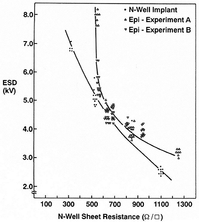
Figure 1. ESD robustness as a function of retrograde n-well sheet resistance for 0.5 μm CMOS technology (With permission from the ESD Association).
It was found that with high energy MeV implanters, the n-well dose could be increased significantly without degradation to the performance. As a result, with technology scaling, it was found that the retrograde implant dose could be increased as the dimensions were scaled; this lead to significant reduction of CMOS latchup concerns (Voldman and Gross, 1993; Voldman, 1994a,b).
Isolation
Evolution of the isolation technology had a significant change in the ESD scaling. The most significant transition was the migration from LOCOS isolation to shallow trench isolation (STI).
Locos Isolation
Early technology development introduced LOCOS isolation to define device active regions for MOSFETs, and contacts. LOCOS isolation was formed on the surface, where half of the structure was below the semiconductor substrate surface, and half of the structure was above the substrate surface.
In this technology, the source and drain junctions was formed deeper than the bottom of the LOCOS isolation. This introduced lateral parasitic p-n diodes, as well as npn and pnp bipolar junction transistor (BJT). From an ESD perspective, this provided lateral parasitic devices to discharge ESD and EOS current. This allowed for lateral current flow, and also allowed lateral heat flow in the substrate. On the other hand, it also introduced parasitic devices that lead to ESD failure.
Shallow Trench Isolation
Shallow trench isolation (STI) technology development began in the mid-1980's and introduced in the IBM 0.25-μm in both DRAM and logic technology (Maloney, 1988; Voldman and Gross, 1993; Voldman, 2004, 2015). With the introduction of the STI, lateral parasitic device bipolar current gain was significantly reduced, with essentially eliminated the parasitic device. Secondly, the STI structure constrained thermal diffusion along the substrate surface leading to higher surface temperatures during ESD events.
In STI technology, the peak heating of a lateral p-n diode occurs under the STI bottom between the p- and n-regions (Figure 2). As the well doping concentration is increased, the resistance and the heating is reduced, leading to improved ESD protection (Voldman and Gross, 1993). Failure analysis also shows that the damage is in the region of peak heating which occurs under the isolation (Never and Voldman, 1995).
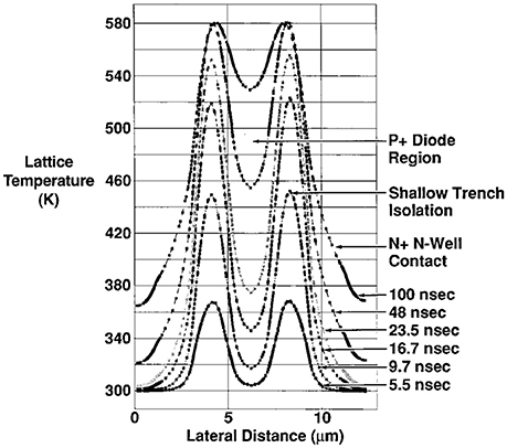
Figure 2. Simulation of ESD event in p+/n+ diode with 0.55 μm deep shallow trench isolation (with permission from the ESD Association).
Figure 3 shows that the peak lattice temperature is highest for a semiconductor process with a STI and retrograde well (Voldman, 2004). In LOCOS isolation and a diffused well process, the Joule heating is lowest because of the lateral thermal diffusion. In a LOCOS technology, with a retrograde well, there is more resistance in the well region near the LOCOS surface. In STI, the isolation structure leads to both lack of lateral current flow, and current crowding under the isolation region.
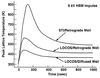
Figure 3. Peak Lattice Temperature for processes with different isolation structures for 0.25 μm CMOS technology (with permission from the ESD Association).
MOSFET Source/Drain
MOSFET source/drain junctions have evolved to address reliability and performance objectives. The evolution of the MOSFET source/drain regions included abrupt junctions, low doped drains (LDD), and extension implants.
Abrupt Junctions
In early MOSFET development, only a single implant was introduced for a MOSFET source and drain implant. A single implant lead to hot electron issues and punch-through as the MOSFET channel length was reduced. With abrupt junctions, MOSFET source/drain structures had low self-heating in the MOSFET source and drain.
LDD Junctions
Lightly doped drain (LDD) structures were introduced in MOSFETs to reduce the effect of hot electrons. With the introduction of MOSFET LDD implants, the electric field near the drain-channel region is reduced. The lowering of the electric field lowered the probability of hot electron injection in a MOSFET. Figure 4 shows an atomic force microscope (AFM) image of a 0.35 um series cascode MOSFET in a 0.35 um technology after an ESD event (Voldman, 2009).
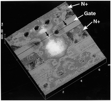
Figure 4. MOSFET second breakdown in cascoded NFETs in a 0.35 μm technology (with permission from the ESD Association).
With the introduction of silicide layers, and the LDD junction, Joule heating occurred in LDD region during ESD events. ESD failure occurred in the LDD region, leading to a significant reduction of the ESD protection level of the MOSFET. The HBM ESD robustness decreased by approximately a factor of 2.
ESD Implant
To avoid Joule heating within the LDD region of a MOSFET, an additional implant was added to eliminate the ESD degradation concern. An “ESD implant” was placed selectively in the LDD region to eliminate the degradation concern. This was used in technology generations after abrupt junctions, and before introduction of extension implants.
Extension Implants
Extension implants were added to MOSFET source/drain structure to provide a low resistance region near the MOSFET gate and spacer region and avoid the self-heating introduced from the low doped drain (LDD) implant. Extension implants allowed for continued scaling of the MOSFET channel length without MOSFET punch-through.
Silicides
In order to lower the series resistance of the MOSFET source and drain regions, silicide was deposited in the source and drain region. In the MOSFET source/drain structure, the current flows through the silicide region instead of the diffusion. This can lead to Joule heating in the MOSFET.
Titanium Silicide
Titanium silicide was introduced into 0.5-μm CMOS technology. Titanium silicide has two states, a high resistance and low resistance state. With proper semiconductor processing, titanium silicide will undergo a low resistance state. A phase transformation occurs between the polymorphic C49 to C54-TiSi2 state. It is desired to provide the C54-TiSi2 state for semiconductor technology (Never and Voldman, 1995).
When an ESD event occurs, the failure analysis demonstrates the change in resistance state in the region of high current region of the device. Figure 5 shows a CMOS diode after an ESD event. The change of state is observable in diodes and MOSFET structures (Voldman, 2002).
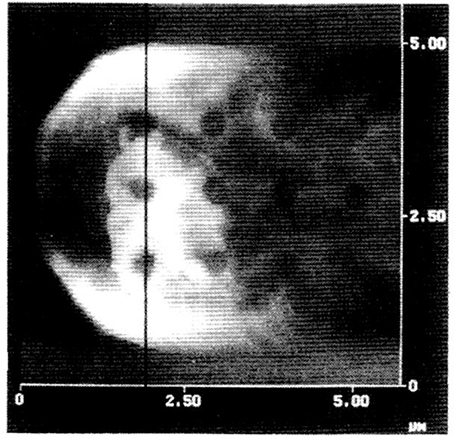
Figure 5. Titanium silicide damage in 0.5 μm CMOS technology (with permission from the ESD Association).
The process window for achieving lower sheet resistance on narrow lines is shrinking with each technology generation due to reduced widths and thinner films. As a result, new silicide materials are needed with technology scaling (Voldman, 1999a; Voldman et al., 2000a,d).
Cobalt Silicide
To provide a lower sheet resistance for scaled advanced technologies, Cobalt silicide is used to replace the Titanium silicide. Cobalt responds differently than Titanium to ESD and EOS high currents. Cobalt silicide has a tendency to agglomerate on the surface. Cobalt has a lower melting temperature than Titanium, but served as a suitable solution for ESD in narrow lines.
Silicide Block Masks
To prevent the current flowing through the silicide region, masks were introduced to block the silicide formation in the MOSFET source/drain. With the use of silicide block masks, electro-current constriction is reduced in the MOSFET source or drain region. As a result, with silicide block masks, the ESD robustness for a MOSFET is improved by providing uniform current distribution and resistor ballasting through the entire structure. Silicide block masks of the drain was utilized across the industry as a common design practice to provide good ESD protection in MOSFET structures.
MOSFET Gate Dielectrics
MOSFET gate dielectrics are prone to failure from the charged device model (CDM) events. During a CDM event, the substrate or power supply is charged. An input pin is grounded, causing the current to flow back to the grounded pin. The CDM current will flow through any component back to the grounded location. The ESD current can penetrate through the gate dielectric leading to a “pin hole” in the MOSFET gate, as shown in Figure 6. To avoid CDM issues, ESD circuitry can be added to the receiver circuit, avoiding MOSFET gate dielectric failure (Voldman, 2009).
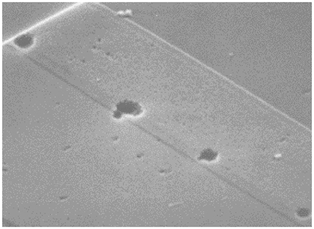
Figure 6. Charged device model (CDM) damage in 100A MOSFET gate oxide (with permission from John Wiley and Sons, Ltd).
With MOSFET scaling, the dielectric breakdown voltage decreases, making it more difficult to protection thin film dielectrics. This is solved with improved ESD circuitry, resistor elements, and spatial dependency between the ESD structure and the MOSFET gate.
Via and Interconnect Technology Evolution
Interconnect and via technology evolution occurs with the scaling of technology. The interconnect and via technology must keep step with the density and performance objectives of a technology. With dimensional scaling of the device, the interconnects must also be scaled as well. Interconnect scaling is required for electrical characteristics (e.g., resistance and capacitance) but also dimensional issues.
Tapered Aluminum Vias
In early CMOS technology, the via technology was a tapered via. A interlevel-dielectric (ILD) layer was etched to the silicon wafer surface to establish the connection between the silicon junction and the interconnect. The via was formed using a deposition of aluminum film over the entire line length and the opening for the via. In early development, the aluminum line and the via was a single non-planar film. In this process, there was no refractory film.
The reliability concern with this technology, was “aluminum spiking.” With EOS, or ESD, the aluminum metal would penetrate into the source and drain region, and eventually the metallurgical junction. The penetration of the aluminum into the junction would lead to increased leakage current.
Tungsten Stud Contacts
As technology advanced, the tapered via was replaced by tungsten studs. Tungsten contacts were introduced replacing the tapered aluminum via technology. Tungsten has a high melting temperature compare to aluminum. Tungsten melts at 3,400°C, whereas aluminum melts at 660°C. The tungsten contact failure did not occur from 0.8 μm to 45 nm. Figure 7 shows the first evidence of a tungsten stud failure.
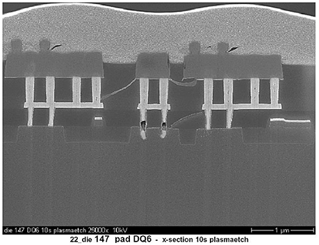
Figure 7. Tungsten stud ESD failure in 45 nm CMOS technology (with permission from the ESD Association).
Interconnects
As technology scaled, the number of input/output (I/O) circuits increased. According to Rent's Rule, as the number of circuits increase on a semiconductor chip, the number of I/O increases. With the increase in the I/O circuits, the interconnects that connect the signal pads to the circuits must be reduced in width. Additionally, the film thickness is decreased to reduce the line-to-line capacitance coupling that leads to cross-talk (Voldman, 1997, 1999b; Voldman et al., 1998, 1999b).
Aluminum Interconnects
As the Ti/Al/Ti wiring decreases in width, the interconnect failure became the limiting failure mechanism in high pin count semiconductor chips (Voldman, 1997, 1999b). In the failure of a Ti/Al/Ti interconnect, the first event that occurs is the aluminum melts due to the melting temperature of aluminum is 660°C. The second event is the inter-level dielectric (ILD) on the sidewall of the Ti/Al/Ti cracks allowing the aluminum to flow laterally into the ILD region. With the aluminum flowing out of the region, the current flows through the Ti films. Titanium failure occurs when the melting temperature of Titanium is reached.
Copper Interconnects
Copper interconnects were introduced by IBM for CMOS technology (Voldman, 1998). From an ESD perspective, copper interconnects have a superior ESD robustness due to the copper melting temperature is higher than aluminum by approximately a factor of 2 (Voldman, 1997, 1999b; Voldman et al., 1998, 1999b). Copper interconnects were introduced by etching a trough into an inter-level dielectric (ILD), depositing a refractory metal film, filling with copper, and then chemical mechanical polishing (CMP). Figure 8 shows failure of a copper interconnect.
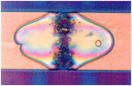
Figure 8. Copper interconnect failure in first technology with Cu interconnects (with permission from the ESD Association).
In Figure 9, the plot shows the critical current to failure (Jcrit) as a function of the pulse width, for both aluminum and copper interconnects (Voldman, 1997, 1999b; Voldman et al., 1998, 1999b). As the pulse width decreases, the critical current to failure increases. Figure 9 demonstrates that copper interconnects have approximately a 2X increase in ESD and EOS robustness compared to aluminum interconnects.
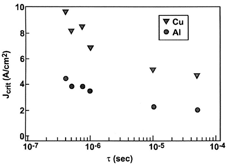
Figure 9. Comparison of critical current to failure for copper and aluminum interconnects in 130 nm CMOS technology (with permission from the ESD Association).
Inter-level Dielectrics
Inter-level dielectrics play a role in the ESD and EOS robustness of interconnects. As current flows through an interconnect, the Joule heating occurs in the wiring. Heat diffuses from the wire interconnect into the surrounding dielectrics. The ILD layer provides a sheath to absorb and diffuse the heat from the interconnect. Hence the type of material of the dielectric material plays a role in the ESD and EOS robustness of the interconnect.
SiO2 ILD
Historically, the inter-level dielectric in semiconductors was silicon dioxide (SiO2). Silicon dioxide surrounds the metal interconnect on all sides. Silicon dioxide allowed for the heat to flow into insulator, lowering the failure level of the interconnect. For long pulses, such as EOS events, heat has a longer time to diffuse into the insulator region.
Low-K ILD
To lower the cross-talk between adjacent lines, different dielectric materials were used to reduce the line-to-line capacitance. The low-K materials also have a lower thermal resistance, preventing the heat to diffuse into the insulator regions. Figure 10 shows an example of a copper interconnect in both SiO2 and a low-K material (Voldman et al., 1999b). What is observed is that the Cu interconnect in a low-K material has a lower current density to failure.
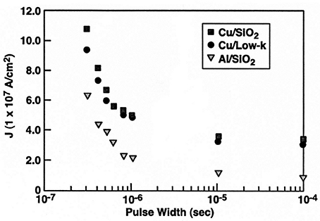
Figure 10. ESD robustness of interconnects in low-K material in a 130 nm CMOS technology (with permission of the ESD Association).
Silicon on Insulator (SOI) Technology
Silicon on insulator (SOI) technology was a niche technology that was used in military and space applications. In order to maintain Moore's Law, there was a belief in the industry that SOI technology would be a natural migration of bulk CMOS technology. In the 1990's, IBM began developing microprocessors in SOI technology, with an introduction in 2000 in IBM mainframes.
One of the concerns with SOI technology was the ability to provide ESD protection (Voldman, 2004, 2009, 2015). It was believed that ESD protection would be lowered due to the elimination of a substrate diode preventing current discharge to the substrate wafer. It was shown that excellent ESD protection was achievable is SOI microprocessors with introduction of a later SOI device (Figure 11) (Voldman et al., 1999a; Voldman, 2004, 2009, 2015).
Figure 11. Silicon on insulator (SOI) protection device for 0.25 μm SOI technology (with permission of the ESD Association).
One of the advantages of SOI technology is that the individual fingers of a SOI structure are separated from substrate region, leading to an improvement in the uniformity of the ESD discharge. Figure 12 shows the damage of a lateral diode string ESD network in SOI, which exhibits uniformity in the first diode element connected to the input pad (Voldman, 1999a, 2004; Voldman et al., 1999a,b, 2000a).
Figure 12. Silicon on insulator (SOI) failure mechanism in a 0.25 μm CMOS SOI technology (with permission from the ESD Association).
Silicon Germanium Technology
Silicon Germanium (SiGe) technology introduced a hetero-junction bipolar transistor (HBT) for radio frequency (RF) applications (Voldman et al., 2000b,c,d, 2002). Figure 13 shows an example of a 47 GHz Silicon Germanium HBT device. SiGe HBT devices is the primary active device in an SiGe RF technology. With technology scaling, faster devices were introduced in successive technology generations. The successive devices introduced a 90, 120, and 200 GHz SiGe HBTs.
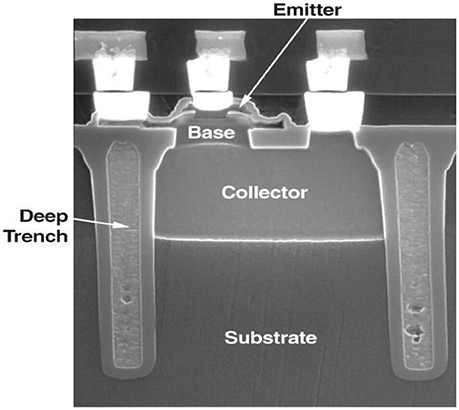
Figure 13. Silicon Germanium (SiGe) 45 GHz HBT device in a 0.35 μm technology (with permission from the ESD Association).
ESD protection of a SiGe RF technology required a different ESD library and ESD design strategy compared to a CMOS technology. The RF ESD library required RF models of all elements used for ESD protection, as well as a CadenceTM based design system.
Figure 14 shows an example of a transmission line pulse (TLP) I-V characteristics of a Silicon Germanium transistor (Voldman et al., 2000b,c,d, 2002; Voldman, 2006). From the TLP measurement, the first and second breakdown of the device is observed.
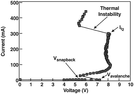
Figure 14. SiGe 45 GHz HBT TLP I-V characteristic (with permission from the ESD Association).
In this plot, the critical current to failure (Jcrit) vs. pulse width is shown for a SiGe HBT, and a Si BJT device (Voldman et al., 2000d; Voldman, 2004). From the results, the SiGe HBT has significantly better results for shorter pulse events (Figure 15).
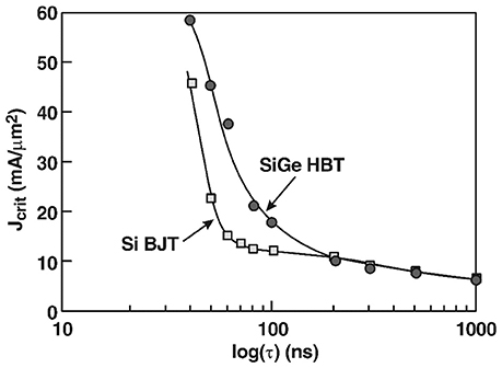
Figure 15. SiGe HBT and Si BJT comparison (with permission from the ESD Association).
Advanced Technology Nodes
Bulk CMOS FinFETs
In the advanced technology nodes, a new device is introduced known as FinFETs (Figure 16). In a FinFET structure, the channel is separated into narrow regions in parallel MOSFET fingers. As a result, the ESD response of a FinFET will be significantly different from a MOSFET. Early FinFET ESD results show that the ESD event is isolated to a number of fingers but not the entire device. The failure of the structure will be a function of different design variables distinct from a planar MOSFET.
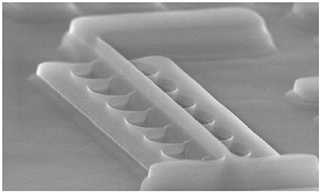
Figure 16. FinFET device (with permission from John Wiley and Sons Ltd).
SOI FinFET
Advanced semiconductor nodes may use an SOI FinFET instead of a bulk FinFET. One of the concerns in SOI is self-heating within the SOI device channel region. In future technologies, as the buried oxide film is scaled, the self-heating will be less of an issue. At this time, it is not clear which implementation will be favored in future technology generations.
Packaging
EOS events can be a concern for the packaging (Voldman, 2005, 2013). The packaging must be able to disperse the energy without failure. Figure 17 shows an example of an EOS event where the package began to melt. EOS events can lead to failures in the package from the bond pads, wire bonds, and plastic packaging issues (Voldman, 2013).
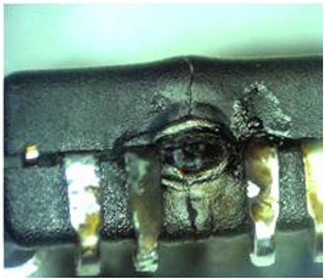
Figure 17. EOS packaging failure (with permission from John Wiley and Sons Ltd).
Multi-Chip Modules
ESD and EOS is a challenge in multi-chip modules. Multi-chip applications can include a carrier, an interposer, and multiple chips. In the assembly and handling of the components of the multi-chip application, charging can occur that leads to ESD failure. In multi-chip applications, where the chips are spaced adjacent to each other, chip-to-chip ESD failure can occur. ESD events can also occur between the chips that involve the carrier or interposers. Handling and assembly procedures may be needed to avoid these concerns.
D Packaging Technology
In multi-chip environments, where chips are placed adjacent to each other, charging processes can occur in the assembly of 2.5-D packaging application. In 2.5-D systems, the interconnection can occur using a large amount of wire-bonds between the chips. The wire bonds can be prone to EOS failure in the 2.5-D assembly.
3-D Packaging and Through Silicon Vias (TSV)
In multi-chip 3-D packages, ESD and EOS events can occur. In early development of the multi-chip assemblies, prior to through silicon vias (TSV) development, charging occurred between chips that were separated by an insulator. In these assemblies, the stored charge between the chips was on the order of 200 pF. This issue may be mitigated with the introduction of TSVs into the multi-chip 3-D assembly. Even with the presence of TSV structures between chips, there must still require an assembly process that avoids charging concerns.
Future Challenges
Future challenges will exist to avoid ESD and EOS concerns in advanced technology, and future chip and system assembly. With new devices, new materials, and new assemblies, there will still be significant work to understand the ramifications of EOS and ESD.
Conclusion
Since 1980, there has been tremendous growth of knowledge in EOS and ESD, to be able to address these concerns, and mitigate issues in future technologies. Although the issues will still be present, with the increase in understanding, the impact can be minimized.
Author Contributions
The author confirms being the sole contributor of this work and approved it for publication.
Conflict of Interest Statement
The author declares that the research was conducted in the absence of any commercial or financial relationships that could be construed as a potential conflict of interest.
References
Alexander, D. R., and Enlow, E. W. (1981). Predicting lower bounds on failure power distributions of silicon NPN transistors. IEEE Trans. Nucl. Sci. NS-28, 4305–4310.
Ameresekera, A., and Duvvury, C. (1994). The impact of technology scaling on the ESD robustness and circuit design, in Proceedings of the EOS/ESD Symposium (Las Vegas, NV), 237–245.
Arkihpov, V. I., Astvatsaturyan, E. R., Godovosyn, V. I., and Rudenko, A. I. (1983). The power to failure model for cylindrical defect. Int. J. Electr. 55:395.
Ash, M. (1983). Semiconductor junction non-linear failure power thresholds: wunsch-bell revisited, in EOS/ESD Symposium (Las Vegas, NV), 122–127.
Brown, W. D. (1972). Semiconductor device degradation by high amplitude current pulses. IEEE Trans. Nucl. Sci. NS-19, 68–75.
Dwyer, V. M., Franklin, A. J., and Campbell, D. S. (1989). Thermal failure in semiconductor devices. Solid State Electr. 33, 553–560.
Enlow, E. N. (1981). Determining an emitter-base failure threshold density of NPN transistors, in EOS/ESD Symposium (Las Vegas, NV), 145–150.
Greve, D. W. (1981). Programming mechanism of polysilicon fuse links, in International Electron Device Meeting Technical Digest (Washington, DC), 70–74.
Lin, D. (1993). ESD sensitivity and VLSI technology trends: thermal breakdown and dielectric breakdown, in Proceedings of the EOS/ESD Symposium (Las Vegas, NV).
Maloney, T. J. (1988). Designing MOS inputs and outputs to avoid oxide failure in charged device model, in Proceedings of the EOS/ESD Symposium (Orlando, FL).
Never, J., and Voldman, S. (1995). Failure analysis of shallow trench isolation ESD structures, in Proceedings of the Electrostatic Overstress/Electrostatic Discharge (EOS/ESD) Symposium (Phoenix, AZ).
Pierce, D., and Mason, R. (1982). A probabilistic estimator for bounding transistor emitter-base junction transient-induced failures, EOS/ESD Symposium (Orlando, FL), 82–90.
Smith, J. S., and Littau, W. R. (1981). Prediction of thin-film resistor burn-out, in Electrical Overstress and Electrostatic Discharge Symposium Proceedings (Las Vegas, NV), 192–197.
Tasca, D. M. (1970). Pulse power failure modes in semiconductors. IEEE Trans. Nucl. Sci. NS-17, 346–372.
Vlasov, V. A., and Sinkevitch, V. F. (1971). Pulsed power physical model for a point defect. Elektronnaya Technika 4, 68–75.
Voldman, S. (1994a). Optimization of MeV retrograde wells for advanced logic and microprocessor/powerPC and electrostatic discharge (ESD), in Invited Talk, Smart and Economic Device and Process Designs for ULSI Using MeV Implant Technology Seminar: SEMICON West, SEMICON West GENUS Seminar (San Francisco, CA).
Voldman, S. (1994b). Retrograde well implants and ESD, invited talk, in SEMATECH Vertical Modulated Well PTAB (Austin, TX).
Voldman, S. (1997). ESD robustness and scaling implications of aluminum and copper interconnects in advanced semiconductor technology, in Proceedings of the Electrostatic Overstress/Electrostatic Discharge (EOS/ESD) Symposium (Orlando, FL), 316–329.
Voldman, S. (1998). The impact of MOSFET technology evolution and scaling on electrostatic discharge protection review paper. Microelectr. Reliab. 38, 1649–1668.
Voldman, S. (1999a). Electrostatic discharge (ESD) protection in silicon-on-insulator (SOI) CMOS technology with aluminum and copper interconnects in advanced microprocessor semiconductor chips, in Proceedings of the Electrical Overstress/Electrostatic Discharge (EOS/ESD) Symposium (Orlando, FL), 105–115.
Voldman, S. (1999b). The impact of technology evolution and scaling on electrostatic discharge (ESD) protection on high-pin-count high-performance microprocessors, in International Solid-State Circuits Conference Proceedings, Session WA21 (San Francisco, CA).
Voldman, S. (1999c). The state of the art of electrostatic discharge protection: physics, technology, circuits, designs, simulation and scaling. IEEE Trans. Solid State Circ. 34, 1272–1282. doi: 10.1109/4.782088
Voldman, S. (2002). Electrostatic discharge (ESD) and failure analysis: models, methodology, and mechanisms, in Proceedings of the International Symposium on the Physical and Failure Analysis of Integrated Circuits (Singapore), 57–65.
Voldman, S. (2003). The impact of technology evolution and revolution in advanced semiconductor technologies on electrostatic discharge (ESD) protection. Keynote talk, in Proceedings of the Taiwan Electrostatic Discharge Conference (T-ESDC) (Hsinchu), 2–9.
Voldman, S. (2005). A review of CMOS latchup and electrostatic discharge (ESD) in bipolar complimentary MOSFET (BiCMOS) silicon germanium technologies: Part I-ESD. J. Microelectr. Reliab. 1, 323–340.
Voldman, S. (2008). Electrostatic discharge and technology scaling: the future of ESD protection in advanced technologies, in International Conference on Solid State and Integrated Circuit Technology (Beijing).
Voldman, S. (2013). Electrical Overstress (EOS): Devices, Circuits and Systems, John Wiley and Sons, Ltd.
Voldman, S. (2016a). Electrostatic discharge (ESD) and electrical overstress (EOS): the state of the art in components to systems. Khoen-Kaen university (KKU)-ENJ J. 1, 25–25.
Voldman, S., Gauthier, R., Reinhart, D., and Morrisseau, K. (1998). High current transmission line pulse characterization of aluminum and copper interconnects for advanced CMOS semiconductor technologies, in Proceeding of the International Reliability Physics Symposium (Phoenix, AZ), 293–301.
Voldman, S., and Gross, V. (1993). Scaling, optimization, and design considerations of electrostatic discharge protection circuits in cmos technology, in Proceedings of the Electrostatic Overstress/Electrostatic Discharge (EOS/ESD) Symposium (Orlando, FL).
Voldman, S., Hui, D., Warriner, L., Young, D., Williams, R., Howard, J., et al. (1999a). Electrostatic discharge protection in silicon-on-insulator technology, in Proceedings of the IEEE International silicon on insulator (SOI) Conference (Napa Valley, CA), 68–72.
Voldman, S., Hui, D., Young, D., Williams, R., Dreps, D., Sherony, M., et al. (2000a). Silicon-on-insulator dynamic threshold ESD networks and active clamp circuitry, in Proceedings of the Electrical Overstress/Electrostatic Discharge (EOS/ESD) Symposium (Anaheim, CA), 29–40.
Voldman, S., Juliano, P., Johnson, R., Schmidt, N., Joseph, A., Furkay, S., et al. (2000b). Electrostatic discharge and high current pulse characterization of epitaxial base silicon germanium heterojunction bipolar transistors, in Proceeding of the International Reliability Physics Symposium (IRPS) (Phoenix, AZ).
Voldman, S., Juliano, P., Schmidt, N., Botula, A., Johnson, R., Lanzeratti, L., et al. (2000c). ESD robustness of a silicon germanium BiCMOS technology, in Bipolar/BiCMOS Circuits and Technology Meeting Symposium (Minneapolis, MN).
Voldman, S., Morriseau, K., Hargrove, M., McGahay, V., and Gross, V. (1999b). High-current characterization of dual-damascene copper interconnects in SiO2 and low-K inter-level dielectrics for advanced CMOS technologies, in Proceedings of the IEEE International Reliability Physics Symposium (IRPS) (Phoenix, AZ), 144–153.
Voldman, S., Ronan, B., Juliano, P., Botula, A., Hui, D., and Lanzerotti, L. (2002). Silicon germanium heterojunction bipolar transistor electrostatic discharge power clamp and the johnson limit in RF BiCMOS SiGe technology. J. Electr. 56, 341–362. doi: 10.1016/S0304-3886(02)00064-5
Voldman, S., Schmidt, N., Johnson, R., Lanzerotti, L., Joseph, A., Brennan, C., et al. (2000d). Electrostatic discharge characterization of epitaxial base silicon germanium heterojunction bipolar transistors, in Proceedings of the Electrostatic Overstress/Electrostatic Discharge (EOS/ESD) Symposium (Anaheim, CA), 239–251.
Keywords: MOSFET scaling, electrostatic discharge, electrical overstress, latchup, scaling theory
Citation: Voldman SH (2018) Evolution, Revolution, and Technology Scaling—The Impact on ESD and EOS Reliability. Front. Mater. 5:33. doi: 10.3389/fmats.2018.00033
Received: 18 January 2018; Accepted: 17 May 2018;
Published: 17 July 2018.
Edited by:
Cher Ming Tan, Chang Gung University, TaiwanReviewed by:
Chun-Yu Lin, National Taiwan Normal University, TaiwanManuel Pereira Dos Santos, Universidade de Évora, Portugal
Copyright © 2018 Voldman. This is an open-access article distributed under the terms of the Creative Commons Attribution License (CC BY). The use, distribution or reproduction in other forums is permitted, provided the original author(s) and the copyright owner(s) are credited and that the original publication in this journal is cited, in accordance with accepted academic practice. No use, distribution or reproduction is permitted which does not comply with these terms.
*Correspondence: Steven H. Voldman, voldman@ieee.org