Work Function Characterization of Potassium-Intercalated, Boron Nitride Doped Graphitic Petals
 Patrick T. McCarthy1,2
 Rajib Paul2†
 Dmitry Zemlyanov2
 Ronald G. Reifenberger2,3
  Timothy S. Fisher1,2*
- 1School of Mechanical Engineering, Purdue University, West Lafayette, IN, United States
- 2Birck Nanotechnology Center, Purdue University, West Lafayette, IN, United States
- 3Department of Physics, Purdue University, West Lafayette, IN, United States
This paper reports on characterization techniques for electron emission from potassium-intercalated boron nitride-modified graphitic petals (GPs). Carbon-based materials offer potentially good performance in electron emission applications owing to high thermal stability and a wide range of nanostructures that increase emission current via field enhancement. Furthermore, potassium adsorption and intercalation of carbon-based nanoscale emitters decreases work functions from approximately 4.6 eV to as low as 2.0 eV. In this study, boron nitride modifications of GPs were performed. Hexagonal boron nitride is a planar structure akin to graphene and has demonstrated useful chemical and electrical properties when embedded in graphitic layers. Photoemission induced by simulated solar excitation was employed to characterize the emitter electron energy distributions, and changes in the electron emission characteristics with respect to temperature identified annealing temperature limits. After several heating cycles, a single stable emission peak with work function of 2.8 eV was present for the intercalated GP sample up to 1,000 K. Up to 600 K, the potassium-intercalated boron nitride modified sample exhibited improved retention of potassium in the form of multiple emission peaks (1.8, 2.5, and 3.3 eV) resulting in a large net electron emission relative to the unmodified graphitic sample. However, upon further heating to 1,000 K, the unmodified GP sample demonstrated better stability and higher emission current than the boron nitride modified sample. Both samples deintercalated above 1,000 K.
Introduction
Carbon nanomaterials exhibit many excellent thermal, optical, and mechanical properties including but not limited to high thermal stability and high optical absorption, making them good candidates for thermionic and photoemission processes (Avouris et al., 2008; Yang et al., 2008; Castro Neto et al., 2009; Westover et al., 2010; Duyvuri et al., 2012). Research in the field of electron emission often focuses on reducing the energy barrier in a material that an electron must overcome for emission, also referred to as the work function. More recent research with carbon materials has investigated the fabrication of nanostructures that can confine electrons, forcing them to higher energy levels, thereby increasing emission intensity (Huang et al., 1995; Fisher, 2001; Tavkhelidze et al., 2006). For example, Obraztsov has performed extensive research in both classical and non-classical field emission of nanostructured carbon materials demonstrating reduced turn-on voltages of field emission and reduced work functions relative to carbon structures with macro or micro scale features (Obraztsov et al., 2000, 2002, 2003). In addition to favorable material properties, the atomic structure of graphite and few-layer graphene allows for intercalation of the lattice with alkali metals (Dresselhaus and Dresselhaus, 2002). Previous work has demonstrated that carbon nanofibers, nanotubes, and nanowalls intercalated with potassium exhibit significantly reduced work functions and are relatively stable near room temperature in vacuum (Robinson et al., 2005; McMullen, 2010; Westover et al., 2010; Vander Laan, 2011).
Carbon-boron nitride lattices [Cx(BN)] represent a newly developed derivative of graphene (Nag et al., 2010; Raidongia et al., 2010). Boron nitride is an insulating material that often takes the form of a planar, hexagonal atomic array akin to graphene. Chemical modification of a carbon lattice with boron nitride results in a material that exhibits semiconductor-like properties (Yuki et al., 2004). Adjusting the chemical composition of the Cx(BN) structure allows for control of the semiconductor’s band gap and electron affinity, offering the possibility for a well tuned single or bi-layer semiconductor structure. The electrical and optical properties of Cx(BN) for a variety of compositions have been characterized by Yuki et al. (2004), and some early electron emission data have been collected by Okada et al. (2006). Yuki et al. showed that the band gap depends directly on carbon composition, with band gaps ranging from 3.4 to 5.3 eV for carbon composition ratios of 30 and 9%, respectively. Photoemission and field emission studies by Okada et al. have produced similar results.
Theoretical studies of lithium and potassium-intercalated boron nitride have been conducted (Okada and Otani, 2010; Altintas et al., 2011). Results suggest that potassium-intercalated h-BN is semimetallic despite h-BN’s insulating nature. Therefore, potassium-intercalated Cx(BN) could exhibit metallic properties, despite the introduction of an insulating material to a graphitic lattice. However, increased interlayer interaction in hexagonal boron nitride (h-BN) compared to graphite is thought to limit intercalation (Altintas et al., 2011). This hypothesis is consistent with results from other studies that have demonstrated reduced carbon oxidation at elevated temperatures of boron nitride doped graphite relative to unmodified graphite (Shen et al., 1999; Dai and Zhang, 2002), suggesting that movement of oxygen between layers is restricted.
The present study reports characterization of electron emission from potassium-intercalated graphitic petals (GPs), and potassium-intercalated boron nitride modified GPs. GPs are several microns in width and length and are normally 5–25 atomic layers thick (Vander Laan, 2011). GP samples consist of large arrays of petals grown on graphitic substrates. As implied by the complex chemical and physical structures of the materials developed in this study, precise characterization is difficult. However, through proper understanding of the underlying physics of electron excitation and emission, details of which are provided in this report, sample work functions, relative emission intensities, and substrate temperature limits can be isolated. In this study, variable temperature electron energy measurements were performed while photoemission was induced via a solar simulator. Photoemission electron energy distributions (PEEDs) recorded during solar simulator illumination allowed for quantification of relative changes in emitter work function and appropriate annealing temperature limits.
Several other techniques were utilized in studying the petal structures and composition. Scanning electron micrographs (SEMs) were employed to understand the surface morphology. Raman spectroscopy was performed in order to better understand defects of the petal surface and to investigate how boron nitride integrates into the graphitic layers. Finally, X-ray photoelectron spectroscopy (XPS) was utilized to isolate the surface chemistry of the samples. Through these chosen characterization techniques, specific sources of electron emission were established, and their respective magnitudes of emission were measured with respect to temperature and time.
Experimental Methods
Graphitic and Cx(BN) Petal Fabrication
Growth of GP arrays occurred on electrode-grade graphite owing to its high electrical/thermal conductivity. The sample size was approximately 10 mm × 5 mm in area with a thickness of 2 mm. A catalyst-free petal growth process was performed in a SEKI AX5200S microwave plasma chemical vapor deposition system utilizing H2 and CH4 feed gases in conditions described previously (Bhuvana et al., 2010; McMullen, 2010; Vander Laan, 2011). The sample was placed atop a 2.5 cm ceramic post in order to promote coupling of the plasma to the sample. The plasma was initiated in 50 sccm of H2 at 10 Torr pressure. No substrate heat was applied, but exposure to the plasma raised the substrate temperature to near 600 K with the sample temperature presumably being higher than that due to a more direct exposure to the plasma. The initial microwave generator power was 300 W. The pressure and generator power were increased stepwise, with pressure increases preceding generator power increases. The pressure was first raised to 20 Torr, and then power to 500 W; then the pressure was taken to 30 Torr, and finally the power was set to 700 W. This stepwise increase ensures that the power is not too great for a given chamber pressure to cause plasma instabilities. Once the final growth conditions were established (30 Torr pressure, 700 W generator power), a flow of 10 sccm of CH4 was added to the H2, and petal growth occurred for 30 min.
Boron nitride modification of the GP arrays was performed following a previously reported procedure utilizing a microwave heat-assisted chemical treatment in a homogenous water solution of boric acid (H3BO3) and urea (CON2H2) (Paul et al., 2012). Afterward, the sample was vacuum treated for 12 h to remove water content. Finally, the sample was annealed in a N2 environment at 1,180 K for 12 h. SEM images of the Cx(BN) petals are provided in Figure 1.
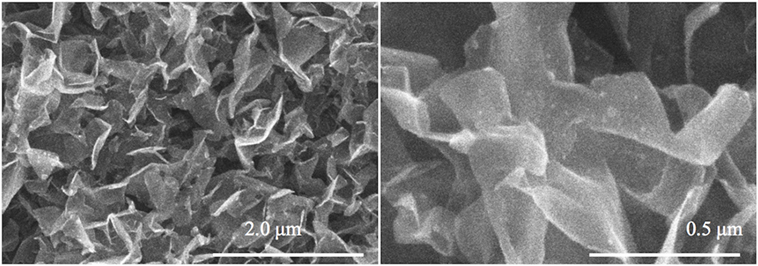
Figure 1. Scanning electron micrograph images of Cx(BN) petals fabricated on electrode graphite.
Raman spectra of the GP and Cx(BN) petal samples are provided in Figure 2. Peaks at approximately 1,360, 1,560, and 2,720 cm−1 correspond to the D, G, and 2D peaks, respectively. The G peak indicates sp2 bonding, while the D peak indicates breaks in sp2 bonds and is commonly referred to as the defect peak (Ferrari, 2007). The 2D peak is the second order harmonic of the D peak. GP arrays have a relative peak intensity ID/IG = 0.67, while the Cx(BN) petal sample exhibits ID/IG = 0.28, suggesting that the boron nitride modification preferentially takes place at the defect sites of the GP arrays.
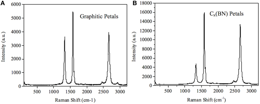
Figure 2. Raman spectra of graphitic petals (GPs) (A) and boron nitride modified GP arrays (B).
Given that potassium reacts readily with water and oxygen, sample loading for potassium intercalation was performed in an inert Ar environment. An Ar-filled glove box was used to load the sample into a sealed glass tube with a pure potassium source. The glass tube was then loaded into a N2-filled tube furnace (Lindberg/Blue M) where a two-step intercalation process was performed (McMullen, 2010; Westover et al., 2010; Vander Laan, 2011). The vessel was first heated to 540 K for 48 h, followed by a second heating process at 340 K for 15 h. The first process vaporizes the potassium source, coating the sample, while the second stage occurs just above the melting temperature of potassium to allow for the physisorbed potassium to diffuse into the petal lattice. Once cooled, the intercalated sample was loaded into a different Ar-filled glass tube without a potassium source prior to testing. The sample was unloaded from the Ar-filled glass tube prior to loading into the vacuum chamber for testing, resulting in exposure to air of several seconds, including additional exposure within the chamber itself prior to air being pumped out of the chamber. All told, several minutes of exposure to air is typical.
X-Ray Photoelectron Spectroscopic Techniques
Chemical composition of the samples was investigated by XPS using a Kratos Axis Ultra DLD spectrometer with monochromatic Al K α radiation (hν = 1,486.58 eV). Survey and high-resolution spectra were collected from a 700 µm × 400 µm spot size in the normal direction with respect to the sample surface. Fixed analyzer pass energies of 160 and 20 eV were used for the survey and high-resolution spectra, respectively. XPS data were analyzed with commercially available CasaXPS software (www.casaxps.com), and individual peaks were fitted to a Gaussian–Lorentzian function. The atomic concentrations of the chemical elements on the near-surface region were estimated after subtraction of the Shirley-type background, taking into account the corresponding Scofield atomic sensitivity factors and inelastic mean free paths of photoelectrons using standard procedures in the CasaXPS software. A charge neutralizer was used for Cx(BN) petals because of their low electrical conductivity, and the resulting spectra were then corrected on the binding energy scale using the position of the main C 1s component at 284.5 eV as a reference for graphitic carbon (Paul et al., 2012).
Electron Emission Theory
In this study, a Newport solar simulator (model 69907 power supply and model 67005 lamp box) with a xenon lamp (model 6255 bulb) and an AM1.5 global filter (model 81094) provides a source of electron excitation for the samples studied. By knowing the wavelength-dependent spectrum of light provided by the solar simulator and utilizing the proper photoemission theory, one can calculate approximate work functions for the materials under study. Figure 3 provides a basic schematic of the photoemission process performed in this report. A solar flux illuminates the sample surface with a spectrum of energy-dependent photons. Photons with energies above the work function (φ) can promote electron emission depending on the direction of emission, while photons below φ will merely heat the surface. An energy analyzer sweeps through specific electron energies such that only emitted electrons within a small energy window are recorded at a particular instant. Given the directionality of electron emission, both low-energy and high-energy photons can contribute to low-energy electron emission, while only high-energy photons can contribute to high-energy electron emission. Therefore, more photons in the solar flux can contribute to the emission of an electron whose final energy state is close to the Fermi energy plus work function (EF + φ) than an electron with final energy state greater than that. A sharp peak in the PEED near EF + φ is generated as a result, with a nearly exponential decay in emission at higher electron energies.
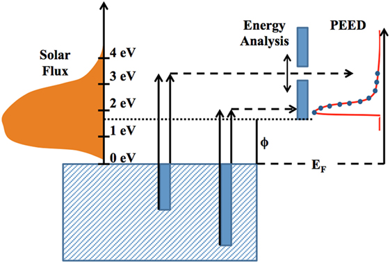
Figure 3. Energy scale schematic of the photoemission process performed in this study.
As indicated in Figure 3, the characteristic shape of the PEED work function reflects a sharp rise in electron emission followed by a smooth exponential-like decaying trailing edge. The energy at which this sharp rise occurs is a reliable measure of the sample work function. The overall shape of the PEED at higher energies generally reflects the decrease in illuminated photons capable of inducing electron emission. With the complex materials developed in this study, multiple rises in electron emission across the PEED and/or a broadening of emission peaks may occur. This behavior is a result of multiple emission sources being present on the surface of the sample, thereby demonstrating several work functions present in the material.
Extraction of one or more work functions from the geometrically complicated and chemically diverse surfaces in this study can be accurately performed via least squares fits to the PEED data of an appropriate photoemission model. The photoemission model below is fit to the experimental PEEDs and best estimates are taken to determine whether a sample exhibits a single emission peak, or multiple emission peaks with the fitting procedure adjusted accordingly. The resulting work functions are considered accurate within ±0.2 eV, accounting for inaccuracies in experimental measurements and data fitting.
Knowledge of thermionic emission theory is critical to developing the photoemission model utilized here. In thermionic theory, electrons are assumed to behave as a free electron gas, and the material is assumed to have a single parabolic conduction band, such that (McMullen, 2010; Westover et al., 2010):
where E is electron energy, ITEED is the thermionic emission intensity, me is the rest mass of an electron, h is Planck’s constant (4.14 × 10⁻¹⁵ eV⋅s), EF is the Fermi level, ϕ is the work function, H is the Heaviside step function, kB is the Boltzmann constant (8.62 × 10⁻⁵ eV/K), and T is temperature.
Photoemission theory can be complicated, but a simplified three-step model is often utilized (Berglund and Spicer, 1964; Spicer and Herreragomez, 1993). Photoemission occurs by: (1) photon penetration and absorption, (2) electron excitation and transport to the surface, and (3) electron emission over the potential barrier (Jensen, 2007). While this is an effective model for many photoemission processes, it requires an extensive knowledge of the material characteristics (e.g., surface geometry, electronic band structure) that are often unknown when studying photoemission properties of newly developed materials.
An alternative model was developed by Westover and McCarthy (Westover et al., 2010; McCarthy et al., 2014) as an extension of the theory developed by Fowler and DuBridge (Fowler and Nordheim, 1928; DuBridge, 1933) and offers a generalized approach for predicting photoemission with regard to specific material properties. As with the thermionic theory embodied in Eq. 1, this model assumes a free electron gas with a single parabolic energy band. Additional assumptions are that photon absorption is independent of photon energy, and that all photon energy is manifested by electron momentum normal to the surface. Given these assumptions, the electron population for a three-dimensional material, described by the Fermi-Dirac function, is simply increased by the photon energy (Vander Laan, 2011):
where IPEED is the photoemission intensity, and ħω is the photon energy. Equation 2 is termed the normal energy model. Westover and McCarthy further improved this model by weighting the number of electrons available for emission based on the angle of electron emission, for which the derivation is provided elsewhere (Westover et al., 2010; McCarthy et al., 2014). The angle of photonic illumination is referenced to the surface normal. The random energy model is given by:
where
Navail,ΔθP is the number of electrons available for emission at a given angle of photonic illumination, W is the energy associated with momentum in the normal direction, and θP is the angle of photonic illumination. A final modification of Eq. 3 is performed in order to account for electron scattering and “smearing” due to the energy analyzer. As these scattering events are not discussed extensively in this report, the details of the scattering theory and additional data related to scattering are provided in Supplementary Material.
By fitting the foregoing photoemission theory to the resulting temperature-dependent PEEDs, electron emission sources from the samples can be isolated and identified as either basic materials (e.g., potassium, graphite, boron-nitride) or newly developed emission sources resulting from potassium intercalation and/or boron nitride modification.
Photoemission Experiments
Photoemission characterization is performed utilizing a SPECS-Phoibos 100 SCD hemispherical energy analyzer (HEA) built into a high-vacuum system. The sample stage has a heater beneath it, with the HEA entrance located 40 mm above the sample. Substrate temperature is monitored by a thermocouple placed beneath the stage. Additionally, at temperatures above 850 K, a pyrometer is used as a secondary temperature measurement. The HEA system records the number of electrons collected per second for a given electron energy. Pressure within the chamber was approximately 2.0 × 10⁻⁸ Torr for room temperature studies, but could rise as high as 3.0 × 10⁻⁷ Torr for substrate temperatures of 1,180 K. A Newport solar simulator (Model 69907 power supply and Model 67005 lamp box) with a xenon lamp (Model 6255 bulb) and an AM1.5 global filter (Model 81094) provides photonic illumination of the samples. The substrate was supplied with a bias of −4 eV to avoid contributions from the detector near 0 eV. The supplied bias was subtracted from all of the data reported here. The chosen bias will impact the intensity of the recorded PEEDs and as such should be kept the same for all studies.
Potassium intercalated within graphite tends to exhibit a high mobility that is temperature dependent. This mobility causes deintercalation of the sample, thereby reducing the effectiveness of the sample as an electron emitter. It is, therefore, important to evaluate emission intensity and sample stability with respect to temperature. Shifts in emission peaks, changes in PEED shapes, and multiple work function peaks often develop over multiple heating cycles. The first heating cycle in particular could produce large changes in PEEDs with temperature, as oxides formed on the sample surface during pretreatment and transfer to the vacuum chamber presumably bake off. In order to investigate the sample work functions and temperature limits of the samples in this study, a systematic heat treatment schedule was developed. Four heating cycles of the samples were performed over 4 days (one per day). A cycle consisted of heating from room temperature to a selected maximum temperature, at which point the sample was allowed to cool to room temperature overnight. The next cycle would begin the following day. Each day, PEEDs were recorded at room temperature (310 K) and then at 100 K intervals starting at 380 K. The selected maximum temperatures for cycles 1–4 were 580, 780, 980, and 1,180 K, respectively. For example, cycle 1 was performed on day 1 with recordings taken up to a maximum temperature of 580 K. Cycle 2 was performed on day 2 with testing up to a maximum temperature of 780 K, and so on. Figure 4 provides the temperatures at which measurements were performed each day.
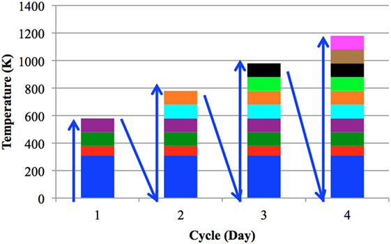
Figure 4. Photoemission temperature measurements during each recording cycle (day).
Results and Discussion
XPS Results
Three main samples were tested via XPS. The first sample consisted of GP arrays grown on electrode graphite. A Cx(BN) petal sample was tested second. The last sample was also Cx(BN) petals but was intercalated with potassium [Cx(BN)-K]. Figures 5 and 6 display X-ray photoelectron survey spectra performed on the GP, Cx(BN) petal, and Cx(BN)-K petal samples. Table 1 contains the elemental compositions derived from XPS analysis of all three samples. High concentrations of boron and nitrogen are detected in the Cx(BN) petal samples, but as a byproduct of the acid treatment, a significant amount of oxygen is also present. Oxygen content is potentially detrimental to sample performance, partially because of the rapid oxidation of potassium. The increase in oxygen content of the Cx(BN)-K petal sample relative to the Cx(BN) petal sample is likely a result of oxidized potassium on the surface.
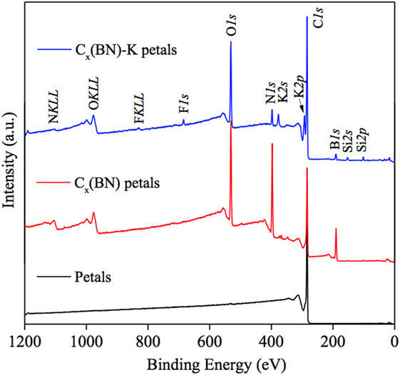
Figure 5. X-ray photoelectron spectroscopy survey analysis of graphitic petals, Cx(BN) petals, and Cx(BN)-K petals.
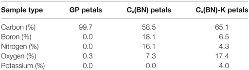
Table 1. Elemental compositions of graphitic petals (GPs), Cx(BN) petals, and Cx(BN)-K petals derived from XPS studies.
Figure 6 contains the fitted C 1s spectra for graphitic petals, Cx(BN) petals, and Cx(BN)-K petals together with the K 2p spectrum for Cx(BN)-K petals. Negligible amounts (≈1 at %) of fluorine and silicon were detected in the XPS analysis of the Cx(BN)-K petals that were most likely introduced during sample handling in the glove box.
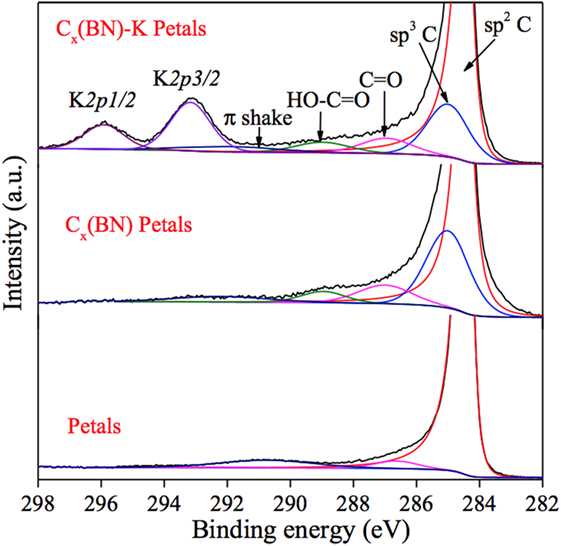
Figure 6. C1S and K2p spectra for graphitic petals, Cx(BN) petals, and Cx(BN)-K petals.
Photoemission Characterization Results
A GP array grown on electrode graphite was intercalated with potassium (GP-K) and was studied in this effort along with a potassium-intercalated boron nitride modified petal sample [Cx(BN)-K]. Results from the first heating cycle (day 1) are presented in Supplementary Material. Data resulting from the first heating cycle are not discussed in detail here as significant variation in PEEDs occurred owing to oxidized surface product bake off from the samples. This oxidation is largely removed during the first heating cycle, allowing for more consistent emission. Figure 7 contains PEEDs from potassium-intercalated samples illuminated by the solar simulator, and associated theoretical fits corresponding to PEED theory, from the second heating cycle (day 2: up to 780 K substrate temperature). The second heating cycle promotes annealing of the petal surfaces, the benefits of which are demonstrated during later heating cycles. Detailed results of the fitted data are provided in Supplementary Material. Plots are normalized for a given set of samples with respect to the PEED with the highest emission peak. Multiple work functions and shifts in peak locations are prevalent with changes in temperature. The maximum emission intensity for each sample occurred between 480 and 580 K. Above 580 K, large reductions in emission were evident with the GP-K sample. For the Cx(BN)-K petal sample, a second high-energy peak emerged above 580 K, coinciding with a significant reduction in low-energy electron emission.
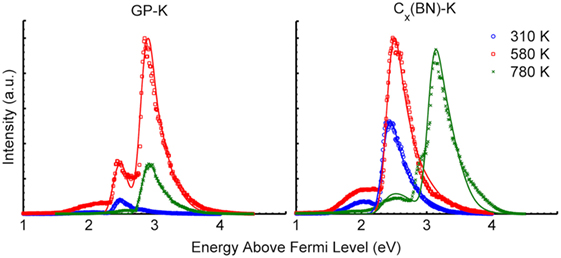
Figure 7. Photoemission electron energy distributions recorded at 310, 580, and 780 K during the second heating cycle of AM1.5 solar simulator illuminated potassium-intercalated GP-K petal and Cx(BN)-K petal samples. Corresponding fits from theory are also plotted.
Three distinct emission peaks occurred during these studies. The first work function is 2.3 ± 0.2 eV, the second is 2.8 ± 0.2 eV, and the third is 3.3 ± 0.2 eV. Given that the work function of bulk potassium is approximately 2.3 eV (Osterlund et al., 1999), the dominant emission peak near room temperature during the first two cycles/days of testing likely results from potassium adsorbed on the surface. Osterlund et al. (1999) measured the change in graphite work function with respect to potassium adsorption thickness and showed that a reduction in the graphite work function from 4.7 to 2.6 eV occurred for 0.4-monolayer coverage of potassium. A 1.0-monolayer coverage decreased the work function to 2.3 eV, verifying that ultrathin layers of coverage generate significant reductions in sample work function. The GP-K sample exhibits a photoemission spectrum attributed solely to surface adsorbed potassium at 310 K. Near 580 K, some potassium apparently remains on the surface, but a dominant PEED edge emerges near 2.8 eV, providing good evidence of intercalation. After annealing at 780 K, nearly all potassium has desorbed from the surface with the dominant edge near 2.8 eV indicating that potassium on the petal surfaces has essentially been incorporated (intercalated) into the GPs.
At 310 K, the Cx(BN)-K petal sample exhibits a PEED that is dominated by surface adsorbed potassium, similar to that observed for the GP-K sample. Additionally, presence of a lower energy shoulder suggests that regions of the sample have work functions below 2 eV. As this energy shoulder is far less pronounced in the GP-K sample, its presence is likely attributed to boron nitride incorporated into the petals. Identifying the geometric origin of these low work functions, high-value active surfaces (perhaps petal edges) could be critical to increasing emission intensity. As the temperature increases, the low work function areas (below 2 eV) remain until disappearing near 780 K. The work function for most of the surface shifts to 3.3 eV, rather than the 2.8 eV work function of the GP-K sample. This work function is most likely a result of potassium intercalation, and the increase in work function relative to the GP-K sample can again be attributed to the boron nitride modification. While some charging of Cx(BN) may be present, resulting in a slight shift of the measured work function of Cx(BN), the potassium intercalation of the Cx(BN)-K petal sample should ensure a high electrical conductivity, thereby minimizing charging. Given that the measured work functions arise from potassium, potassium intercalated graphite, and potassium intercalated Cx(BN), the effects of charging were neglected in this study and any inaccuracies were assumed to fall within the ±0.2 eV uncertainty assigned to the work functions reported.
Both samples exhibited repeatable performance after heating to 780 K, but prior to heating above 980 K. Data from the third cycle/day of testing are, therefore, not presented, as those results closely match the PEEDs recorded during the fourth cycle/day of testing. Figure 8 shows solar-induced PEEDs from the potassium-intercalated samples tested in the fourth heating cycle (up to 1,180 K) along with corresponding fits from theory. Figure 8 shows the stability of the GP-K sample after thorough annealing produced by the first three heating cycles. The GP-K sample is very stable during the fourth heating cycle for temperatures below 680 K with a nearly constant work function of 2.8 eV. Emission intensity increases dramatically upon heating to 980 K, with little to no change in work function and PEED shape. This increased emission might be due to the decomposition of potassium oxide (K2O), potassium peroxide (K2O2), and potassium superoxide (KO2) that likely form overnight in a vacuum of 10−8 Torr between testing cycles, but further studies would be required to verify. Upon heating above 980 K, the emission intensity decreases rapidly and the work function increases as potassium deintercalates.
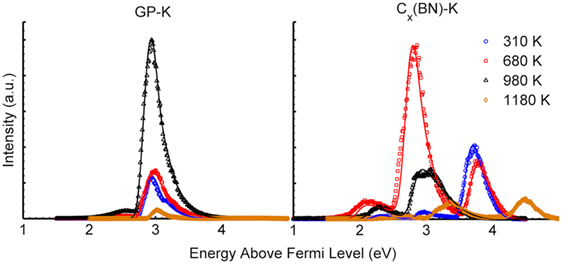
Figure 8. Photoemission electron energy distributions recorded at 310, 680, 980, and 1,180 K during the fourth heating cycle of AM1.5 solar simulator illuminated GP-K petals and Cx(BN)-K petals. Corresponding fits from theory are also plotted.
The Cx(BN)-K petal sample shows an unstable and evolving PEED in the fourth heating cycle, indicative of a highly dynamic surface. The Cx(BN)-K petal sample exhibits low-intensity, high work function emission (approximately 3.5 eV) at room temperature. At 680 K, the PEED shows emission from low work function sites (about 2 eV), a dramatic rise in emission from 2.5 eV work function sites (similar to the activation in the GP-K sample at 980 K), and sites still having a 3.5 eV work function. For temperatures above 680 K, a gradual reduction in emission occurs and similar to the plain GP-K sample, the Cx(BN)-K petal sample rapidly deintercalates above 980 K. Despite this, the Cx(BN)-K petal sample retains multiple work function peaks, even up to 1,180 K where the PEED shows emission from work function sites of 3.3 eV and 4.4 eV, approaching the work function of pristine GPs.
The contrasting PEEDs of the GP-K and Cx(BN)-K petal samples clearly demonstrate that the incorporation of boron nitride in the GPs significantly alters the intercalation of potassium. One possible explanation is that the binding energy of potassium atoms at the carbon and boron nitride interfaces may be higher than its binding energy in non-modified GPs, causing potassium atoms to be pinned. Pinning of potassium atoms to these interfaces may result in increased retention of surface adsorbed potassium on the Cx(BN)-K petal sample relative to the GP-K sample and, in turn, the retention of multiple work functions exhibited in the Cx(BN)-K petal sample PEEDs. Further discussion regarding the origins of these work samples can be found in Supplementary Material.
Conclusion
Thermally assisted photoemission from GPs and boron nitride modified GPs intercalated with potassium was studied in the present work as a method of identifying sample work functions. XPS verified the introduction of boron nitride into the petal lattice. Temperature-dependent PEEDs were recorded over four heating cycles for each sample. Significant changes in the work functions and shapes of the PEEDs were recorded for all samples below 780 K, largely attributed to changes in the surface composition and morphology during the first two heating cycles. After the first two heating cycles, the GP-K sample exhibited a very stable emission peak near 2.8 eV with high-intensity emission at 980 K. While the Cx(BN)-K petal sample was not as stable as the GP-K sample, it did retain three distinct emission peaks throughout the studies, resulting from adsorbed potassium, potassium intercalation, and an unidentified emission source specific to the Cx(BN)-K petal sample. While both samples deintercalated rapidly above 1,000 K, PEEDs from the Cx(BN)-K petal sample indicate that some form of potassium retention does occur relative to the GP-K sample, and perhaps a more precisely manufactured Cx(BN)-K petal material could generate increased electron emission current and provide more thermal stability relative to unmodified GPs.
Further work to explore the origins of the various work functions recorded during these studies is suggested. In particular, regions of low-energy work functions (below 2 eV) are present in small quantities within the Cx(BN)-K petal sample, but their origins have not yet been identified. Furthermore, a rapid rise in electron emission of the GP-K sample between 680 and 980 K during the fourth heating cycle could be of some practical relevance. A similar rise occurs for the Cx(BN)-K petal sample between 380 and 680 K. Understanding the source for this change will allow researchers to better manipulate and control these samples during variable temperature emission.
Author Contributions
As lead author, PM was responsible for graphitic petal growth and potassium intercalation of samples along with performing all experimental emission studies, deriving photoemission theory, and assembling the literature review and report. RP was responsible for boron-nitride treatment of graphitic petals and assisted in the performance of XPS. DZ performed the XPS studies on the samples in this report with RP assisting. RR and TF provided significant support and guidance in the development of this research study, with RR and TF both providing experimental hardware, report editing, and prior knowledge of photoemission theory critical to what was reported here.
Conflict of Interest Statement
The authors declare that the research was conducted in the absence of any commercial or financial relationships that could be construed as a potential conflict of interest.
Funding
This work was supported by the Ingersoll-Rand fellowship provided through the School of Mechanical Engineering, Purdue University. The authors are thankful to the U.S. Air Force Research Laboratory (AFRL), and its Office of Scientific Research (AFOSR) under the MURI program on Nanofabrication of Tunable 3D Nanotube Architectures (PM: Dr. Joycelyn Harrison), as well as the UK-India Education and Research Initiative (UKIERI) through a Trilateral Partnership Grant IND/CONT/2013-14/054, for financial support.
Supplementary Material
The Supplementary Material for this article can be found online at https://www.frontiersin.org/article/10.3389/fmech.2017.00006/full#supplementary-material.
References
Altintas, B., Parlak, C., Bozkurt, C., and Eryigit, R. (2011). Intercalation of graphite and hexagonal boron nitride by lithium. Eur. Phys. J. B 79, 301–312. doi: 10.1140/epjb/e2010-10660-4
Avouris, P., Freitag, M., and Perebeinos, V. (2008). Carbon-nanotube photonics and optoelectronics. Nat. Photonics 2, 341–350. doi:10.1038/nphoton.2008.94
Berglund, C. N., and Spicer, W. E. (1964). Photoemission studies of copper and silver: theory. Phys. Rev. A 136, 1044. doi:10.1103/PhysRev.136.A1030
Bhuvana, T., Kumar, A., Sood, A., Gerzeski, R. H., Hu, J., Srinu, V., et al. (2010). Contiguous petal-like carbon nanosheet outgrowths from graphite fibers by plasma CVD. ACS Appl. Mater. Interfaces 2, 644–648. doi:10.1021/am9009154
Castro Neto, A. H., Guinea, F., Peres, N. M. R., Novoselov, K. S., and Geim, A. K. (2009). The electronic properties of graphene. Rev. Modern Phys. 81, 109–162. doi:10.1103/RevModPhys.81.109
Dai, B. Q., and Zhang, G. L. (2002). A DFT study of hBN compared with graphite in forming alkali metal intercalation compounds. Mater. Chem. Phys. 78, 304–307. doi:10.1016/S0254-0584(02)00205-5
Dresselhaus, M. S., and Dresselhaus, G. (2002). Intercalation compounds of graphite. Adv. Phys. 51, 1–186. doi:10.1080/00018730110113644
DuBridge, L. A. (1933). Theory of the energy distribution of photoelectrons. Phys. Rev. 43, 0727–0741. doi:10.1103/PhysRev.43.727
Duyvuri, B., Kumar, A., Bao, H., Huang, H., Fisher, T., and Ruan, X. (2012). “Thermal radiative properties of vertical graphitic petal arrays,” in Proceedings of the ASME 2010 3rd Micro/Nanoscale Heat & Mass Transfer International Conference, Atlanta, GA.
Ferrari, A. C. (2007). Raman spectroscopy of graphene and graphite: disorder, electron-phonon coupling, doping and nonadiabatic effects. Solid State Commun. 143, 47–57. doi:10.1016/j.ssc.2007.03.052
Fisher, T. S. (2001). Influence of nanoscale geometry on the thermodynamics of electron field emission. Appl. Phys. Lett. 79, 3699–3701. doi:10.1063/1.1421418
Fowler, R. H., and Nordheim, L. (1928). Electron emission in intense electric fields. Proc. R. Soc. Lond. A Math Phys. Sci. 119, 173–181. doi:10.1098/rspa.1928.0091
Huang, Z. H., Cutler, P. H., Miskovsky, N. M., and Sullivan, T. E. (1995). Calculation of local-density of states at an atomically sharp Si tip. J. Vac. Sci. Technol. B 13, 522–525. doi:10.1116/1.588346
Jensen, K. L. (2007). “Electron emission physics,” in Advances in Imaging and Electron Physics, 1st Edn, Vol. 149, ed. K. L. Jensen (Washington, DC: Elsevier), 147–279.
McCarthy, P. T., Reifenberger, R. G., and Fisher, T. S. (2014). Thermionic and photo-excited electron emission for energy conversion processes. Front. Energy Res. 2:54. doi:10.3389/fenrg.2014.00054
McMullen, K. J. (2010). Measurement of Thermionic Electron Emission from Modified Graphene Petals. West Lafayette, IN: MSME, Mechanical Engineering, Purdue University.
Nag, A., Raidongia, K., Hembram, K. P. S. S., Datta, R., Waghmare, U. V., and Rao, C. N. R. (2010). Graphene analogues of BN: novel synthesis and properties. ACS Nano 4, 1539–1544. doi:10.1021/nn9018762
Obraztsov, A., Volkov, A., and Pavlovsky, I. (2000). Field emission from nanostructured carbon materials. Diamond Relat. Mater. 9, 1190–1195. doi:10.1016/S0925-9635(99)00293-9
Obraztsov, A., Zakhidov, A., Volkov, A., and Lyashenko, D. (2003). Non-classical electron field emission from carbon materials. Diamond Relat. Mater. 12, 446–449. doi:10.1016/S0925-9635(03)00060-8
Obraztsov, A. N., Volkov, A. P., Boronin, A. I., and Kosheev, S. V. (2002). Defect induced lowering of work function in graphite-like materials. Diamond Relat. Mater. 11, 813–818. doi:10.1016/S0925-9635(01)00535-0
Okada, K., Kimura, C., and Sugino, T. (2006). Surface properties of boron carbon nitride films treated with plasma. Diamond Relat. Mater. 15, 1000–1003. doi:10.1016/j.diamond.2005.12.028
Okada, S., and Otani, M. (2010). Stability and electronic structure of potassium-intercalated hexagonal boron nitride from density functional calculations. Phys. Rev. B 81, 233401. doi:10.1103/PhysRevB.81.233401
Osterlund, L., Chakarov, D. V., and Kasemo, B. (1999). Potassium adsorption on graphite(0001). Surf. Sci. 420, 174–189. doi:10.1016/S0039-6028(98)00822-X
Paul, R., Voevodin, A. A., Zemlyanov, D., Roy, A. K., and Fisher, T. S. (2012). Microwave-assisted surface synthesis of a boron-carbon-nitrogen foam and its desorption enthalpy. Adv. Func. Mater. 22, 3682–3690. doi:10.1002/adfm.201200325
Raidongia, K., Nag, A., Hembram, K. P. S. S., Waghmare, U. V., Datta, R., and Rao, C. N. R. (2010). BCN: a graphene analogue with remarkable adsorptive properties. Chemistry 16, 149–157. doi:10.1002/chem.200902478
Robinson, V. S., Fisher, T. S., Michel, J. A., and Lukehart, C. M. (2005). Work function reduction of graphitic nanofibers by potassium intercalation. Appl. Phys. Lett. 87, 113707. doi:10.1063/1.2009052
Shen, C. P., Mayorga, S. G., Biagioni, R., Piskoti, C., Ishigami, M., Zettl, A., et al. (1999). Intercalation of hexagonal boron nitride by strong oxidizers and evidence for the metallic nature of the products. J. Solid State Chem. 147, 74–81. doi:10.1006/jssc.1999.8176
Spicer, W. E., and Herreragomez, A. (1993). “Modern theory and applications of photocathodes,” in 1st Conference on Photodetectors and Power Meters, Vol. 2022 (San Diego, CA), 18–33.
Tavkhelidze, A., Bibilashvili, A., and Jangidze, L. (2006). Observation of quantum interference effect in solids. J. Vac. Sci. Technol. B 24, 1413–1416. doi:10.1116/1.2198856
Vander Laan, S. J. (2011). Photonically and Thermally Excited Electron Emission from Modified Graphitic Nanopetals. West Lafayette, IN: MSECE, Purdue University.
Westover, T. L., Franklin, A. D., Cola, B. A., Fisher, T. S., and Reifenberger, R. G. (2010). Photo- and thermionic emission from potassium-intercalated carbon nanotube arrays. J. Vac. Sci. Technol. B 28, 423–434. doi:10.1116/1.3368466
Yang, Z.-P., Ci, L., Bur, J. A., Lin, S.-Y., and Ajayan, P. M. (2008). Experimental observation of an extremely dark material made by a low-density nanotube array. Nano Lett. 8, 446–451. doi:10.1021/nl072369t
Keywords: thermionic, electron emission, photoemission, photoemission spectroscopy, graphene, boron nitride, potassium intercalation
Citation: McCarthy PT, Paul R, Zemlyanov D, Reifenberger RG and Fisher TS (2017) Work Function Characterization of Potassium-Intercalated, Boron Nitride Doped Graphitic Petals. Front. Mech. Eng. 3:6. doi: 10.3389/fmech.2017.00006
Received: 29 April 2017; Accepted: 20 June 2017;
Published: 05 July 2017
Edited by:
David B. Go, University of Notre Dame, United StatesReviewed by:
Tyson Back, University of Dayton Research Institute (UDRI), United StatesFranz A. Koeck, Arizona State University, United States
Copyright: © 2017 McCarthy, Paul, Zemlyanov, Reifenberger and Fisher. This is an open-access article distributed under the terms of the Creative Commons Attribution License (CC BY). The use, distribution or reproduction in other forums is permitted, provided the original author(s) or licensor are credited and that the original publication in this journal is cited, in accordance with accepted academic practice. No use, distribution or reproduction is permitted which does not comply with these terms.
*Correspondence: Timothy S. Fisher, tsfisher@purdue.edu
†Present address: Rajib Paul, Department of Mechanical and Aerospace Engineering, Case Western Reserve University, Cleveland, OH, United States