Reliability of Buried InGaAs Channel n-MOSFETs With an InP Barrier Layer and Al2O3 Dielectric Under Positive Bias Temperature Instability Stress
 Haiou Li1 Kangchun Qu1
  Xi Gao1 Yue Li1 Yonghe Chen1 Zhiping Zhou1 Lei Ma1
  Fabi Zhang1 Xiaowen Zhang1 Tao Fu1
  Xingpeng Liu1 Yingbo Liu1
  Tangyou Sun1*
  Honggang Liu2*
- 1Guangxi Key Laboratory of Precision Navigation Technology and Application, Guilin University of Electronic Technology, Guilin, China
- 2Microwave Device and IC Department, Institute of Microelectronics, Chinese Academy of Sciences, Beijing, China
The positive bias temperature instability (PBTI) reliability of buried InGaAs channel n-MOSFETs with an InP barrier layer and Al2O3 gate dielectric under medium field (2.7 MV/cm) and high field (5.0 MV/cm) are investigated in this paper. The Al2O3/InP interface of the insertion of an InP barrier layer has fewer interface and border traps compared to that of the Al2O3/InGaAs interface. The subthreshold slope, transconductance, and shift of Vg are studied by using the direct-current Id-Vg measurements under the PBTI stress. The experimental results show that the degradation of positive ΔVg under the medium field stress is mainly caused by the acceptor trap, while the donor trap under the high field stress become dominant in the subthreshold region, which leads to the negative shift in Vg. The medium field stress-induced acceptor traps are attributed by the InP barrier layer in the subthreshold region, resulting that the low leakage current can be achieved in the buried InGaAs channel n-MOSFETs with an InP barrier layer compared to the surface InGaAs channel n-MOSFETs.
Introduction
InGaAs was considered for use as the n-type high-mobility channel material because it has higher electron mobility and smaller electron effective mass than that of silicon [1–3]. The complementary metal oxide semiconductor (CMOS) structure can be realized by integrating III-V n-MOSFETs and Ge p-MOSFETs on a Si CMOS platform [4–6]. However, one of the most critical problems that must be solved to realize III-V MOSFETs is the formation of a stable MOS interface with low trap density [7]. Compared with the SiO2/Si system, the III-V native oxides negatively affect fermi-level pinning and current drift [8–10]. The atomic layer deposited (ALD) Al2O3 dielectric in surface InGaAs channel MOSFETs can achieve a thermally stable interface and large band offsets, as confirmed by the previous research on the dielectric layer of InGaAs MOSFETs [11–13]. However, Al2O3/InGaAs interface traps and border traps in the dielectric layer remain high, which reduces the effective channel mobility and results in reliability instability in InGaAs MOSFETs [14–16]. Based on the poor interface quality of InGaAs and Al2O3, the introduction of a barrier layer between the Al2O3 dielectric and InGaAs channel considerably improves channel electron mobility, transconductance, and drive current [17–19]. Although the InGaAs channel and Al2O3 dielectric are separated by the barrier layer, high interface traps and border traps considerably affect device reliability under bias temperature instability (BTI) stress [20–22]. To reduce interface defect density, the interface passivation techniques of N passivation treatment [23–25] and sulfur passivation treatment [26–28] have been investigated to improve the interface properties and reliability.
Bias temperature instability stress directly leads to the degradation of threshold voltage, subthreshold slope, and on-state current. The interface trap and border trap induced by bias temperature instability stress are also considered to be the causes of the degradation of III-V MOSFET performance. Li et al. investigated the surface InGaAs channel n-MOSFETs under positive bias temperature instability (PBTI) stress and recovery [29]. They explained that high defect density exists at the InGaAs and Al2O3 interface, which includes both interface traps and border traps, and the PBTI stress induces mainly border traps. However, few studies have reported the buried channel InGaAs MOSFETs with a barrier layer under PBTI stress.
In this paper, we experimentally studied the mechanisms of the buried InGaAs channel n-MOSFETs with an InP barrier layer under PBTI stress and recovery. The interface and border traps are estimated in the Al2O3/InP and Al2O3/InGaAs interfaces. The degradation of Id-Vg during the PBTI tests shows a shift in Vg under a medium field (2.7 MV/cm), which is the opposite of that observed under a high field (5.0 MV/cm) in buried InGaAs channel n-MOSFETs. The effects of PBTI stress in the buried InGaAs channel n-MOSFETs with an Al2O3/InP interface were investigated by performing the subthreshold slope, transconductance, and Vg shift. The specific border traps are quantified to analyze the reliability of the device under the PBTI stress.
Experimental
Fabrication Process
The main structure of Si-based buried In0.25Ga0.75As channel n-MOSFETs used in this paper is illustrated in Figure 1. The layer structure was grown on InP substrate by metal–organic chemical vapor deposition (MOCVD) and consisted of a 20 nm In0.52Al0.48As buffer layer, a 2 nm In0.6Al0.4As doping layer with Be doping concentration of 3 × 1018 cm−3, a 5 nm In0.52Al0.48As barrier layer, a 5 nm In0.25Ga0.75As channel layer, a 3 nm InP barrier layer, and a 40 nm In0.53Ga0.47As cap layer with N-type doping concentration of 2 × 1019 cm−3. During the device fabrication process, benzocyclobutene (BCB) is used to bond the InP wafer to the Si wafer, and the two-step surface cleaning process was carried out. First, a 10% w/t HCl solution was applied for 1 min to remove the native oxide layer, and 20% w/t NH4OH solution was applied for 6 min. Second, 20% (NH4)2S solution was applied to passivate the interface of the InP barrier layer for 15 min at room temperature [26, 27]. Then, 8 nm of Al2O3 (i.e., gate dielectric) was deposited by Beneq TFS-200 atomic layer deposition (ALD) system at the substrate temperature of 300°C. A postdeposition anneal (PDA) was carried out at 400°C for 30 s in N2 atmosphere. Ti/Au gate metal was evaporated by an electron beam system. The post metal anneals (PMA) at 300°C for 30 s in N2 was carried out in the rapid thermal annealing system. Source and drain electrodes (Ni/Ge/Au/Ge/Ni/Au) were deposited by electron beam evaporation and annealing at 270°C for 3 min. The transistors have a 400-μm channel width and a 4-μm channel length (L).
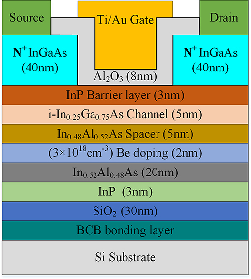
Figure 1. Main structure of buried In0.25Ga0.75As channel n-MOSFETs with 3 nm InP barrier layer and 8 nm Al2O3 gate dielectric.
Measurement Methods
DC current-voltage (I-V) characterization was achieved with an Agilent B1500A semiconductor device analyzer. In the I-V measurements [30], the drain voltage (Vd) was set to 50 mV, and the source and substrate were grounded. During the PBTI stress phase, two different gate voltages were selected during the PBTI stress phase, and the gate field strengths were calculated to be E = 2.7 and E = 5.0 MV/cm, respectively, based on the simulation, while Vs=Vd=Vb = 0 V. All DC Id-Vg tests were carried out at room temperature (300 K). The PBTI test contains a 500 s stress phase and a 500 s recovery phase, as shown in Figure 2. During the stress phase, PBTI stress is set to 2.7 MV/cm and to 5 MV/cm for Al2O3 for a duration of 500 s. Before applying the stress, we first measured the initial Id-Vg curve by using a fresh sample (I-line). After a 500-s PBTI stress, the S line was measured; the R lines were the Id-Vg curves obtained from the sample during the 500 s recovery.
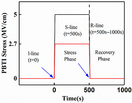
Figure 2. Schematic diagram of the PBTI test setup. The PBTI test contains a 500 s stress phase and a 500 s recovery phase. During the stress phase, PBTI stress is set to be 2.7 and 5.0 MV/cm for Al2O3 for a duration of 500 s.
Results and Discussion
Interface Characteristics
The distribution curves of interface trap density (Dit) are extracted from the multifrequency (1 MHz to 1 KHz) C-V curves of the Al2O3/In0.25Ga0.75As capacitance and Al2O3/InP capacitance, respectively, by using the Castagne-Vapaille method [31], as shown in Figure 3A. Because oxide traps (border trap) near the interface are mainly induced by the PBTI stress [32], InP/InGaAs interface trap can be negligible. The Dit distribution of Al2O3/InP is clearly below that of Al2O3/InGaAs, especially the downtrend of the Dit distribution of the Al2O3/InP interface near the mid-gap and is just opposite to the Dit distribution of the Al2O3/InGaAs interface near the mid-gap. Both Al2O3/InP and Al2O3/InGaAs interfaces are treated with sulfur passivation. The lower interface trap can be realized by employing an InP barrier layer. To further analyze the effect of the slow border trap between Al2O3/InP and Al2O3/InGaAs, the border trap density (ΔNbt) [29] can be described by the C-V hysteresis curve shown in Figure 3B. The ΔNbt distribution of the Al2O3/InP interface is less than that of Al2O3/InGaAs, which indicates that low border traps are achieved in the Al2O3/InP interface.
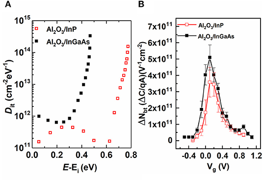
Figure 3. Distribution curves of (A) the interface and (B) border trap densities of Al2O3/InGaAs and Al2O3/InP capacitances extracted from the multifrequency C-V measurement, respectively.
Direct-Current Id-Vg Measurements
Unlike the Si MOSFET under positive bias temperature instability stress, the oxide traps of the InP/Al2O3 are generated during the stress phase. An uninterrupted cycle test on the same device can determine whether the test stress contributes to the Id-Vg curve drift. The Id-Vg curves of the buried InGaAs n-MOSFETs are shown in Figure 4. Compared with a fresh line, there is no distinct shift in Id-Vg curves for either the subthreshold or the on-state region, and there is no clear change in current after the first cycle test. In the second cycle measurement curve, the Id-Vg curves still do not show any shift. The subthreshold slope (SS) and on-state current remain the same compared with the fresh line, which indicates that neither negative nor positive charges were created under the measuring stresses.
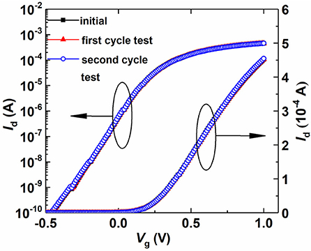
Figure 4. Comparison of DC Id-Vg measurement curves of the buried In0.25Ga0.75As channel n-MOSFETs under different test cycles.
According to the simulation results by Varghese et al. [33], the recoverable donor traps impact negative ΔVg in the subthreshold region. Acceptor traps are essential for inducing a positive I-V curve shift in both the subthreshold and on-state regions. Figures 5A,B show the DC Id-Vg curves measured for the fresh device before stress (I line) and under PBTI stress (S line) (E = 2.7 and E = 5.0 MV/cm) after 500 s as well as the recovery (R line) after 500 s. Compared with the I, S, and R lines in the medium and high fields (2.7 MV/cm and 5.0 MV/cm), there are two cases in the subthreshold region and in the on-state region. (1) In a medium field (E=2.7 MV/cm), the Vg shift ΔVg at a constant drain current is positive both in the subthreshold and on-state regions, which indicates that negative charges were created after the PBTI stress. The Id-Vg curve of the R line still demonstrates a negative shift in the on-state region compared with that of the S line. It is clear that acceptor traps, which are induced by the medium field strength stress, are recoverable. The stress-induced recoverable acceptor traps exist in the on-state region. However, the drain current of the R line coincides with that of S line in the subthreshold region, indicating the medium field strength stress-induced recoverable traps are not shown in the subthreshold region. (2) In a high field (E=5.0 MV/cm), the Vg shift ΔVg is negative in the subthreshold region, indicating donor traps are created after the PBTI stress of 5.0 MV/cm. The Vg shift ΔVg is positive in the on-state region, demonstrating acceptor traps are created after the PBTI stress. The two crossing points, which mean a balance between acceptor trap and donor trap, are founded in 500 s of PBTI and 500 s of recovery with initial curve. The results show that donor traps induce negative Vg shift of Id-Vg curves, larger shift with lower Id current level. The acceptor traps induce positive shift of Id-Vg curves, larger shift with higher Id current level. The high field stress induced donor traps have a large density in distribution of energy gap, and their distribution extends to the conduction band, just opposite to the distribution trend of acceptor traps in the energy gap, which are consistent with that of the surface channel InGaAs n-MOSFETs [29, 33]. By comparing the S line with initial curve under the high field strength stress, the shift of crossing point is found to be negative in the R line with initial curve, indicating the donor traps are almost recoverable. Compared with the S line, the R line demonstrates a negative shift in the on-state region, indicating there are fewer recoverable donor traps than recoverable acceptor traps in the on-state region.
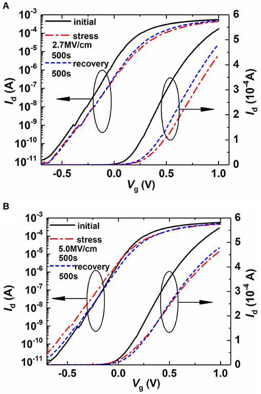
Figure 5. DC Id–Vg curves of buried In0.25Ga0.75As channel n-MOSFETs after (A) 500 s of PBTI stress (E = 2.7 MV/cm) and (B) PBTI stress (E = 5.0 MV/cm) followed by 500 s of recovery.
In surface channel InGaAs n-MOSFETs [29], stress-induced donor traps produce a negative shift in threshold voltage under the 2.7 MV/cm stress. However, stress-induced acceptor traps produce a positive shift in threshold voltage under the 2.7 MV/cm stress in buried channel InGaAs n-MOSFETs. Meanwhile, the Id-Vg curves of the S and R lines do not have an offset in the subthreshold region. The results indicate that no donor traps are induced under medium field for the buried channel device. The Al2O3/InP interface has a lower interface trap density than that of the Al2O3/InGaAs interface in the distribution of energy gap, especially the downtrend of Dit distribution of the Al2O3/InP interface near the mid-gap, which is opposite of the Dit distribution of the Al2O3/InGaAs interface near the mid-gap shown in Figure 3A. The effect of low defect density is not serious in the recovery curve of the buried channel InGaAs n-MOSFETs in the subthreshold region under medium field strength, so buried channel InGaAs n-MOSFETs with Al2O3/InP interface show as a completely different trend than that of surface channel InGaAs n-MOSFETs in the recovery phase.
Time-dependence of ΔVg in the on-state and subthreshold regions is shown in Figures 6A,B respectively. The value of ΔVg shifts to positive direction in the on-state region under medium and high field strengths. From 500 to 1,000 s of recovery, ΔVg of the two recovery curves continues the downward trend in the on-state region. The result shows recoverable acceptor traps have been proved to be recoverable in the on-state region under the field stress. The degradation of negative ΔVg under high field stress is clearly smaller than the degradation of positive ΔVg under medium field stress, indicating donor traps are induced under high field stress in the subthreshold region. Because stress-induced donor traps are fully recovered in the subthreshold region, Vg is totally recovered in the subthreshold region. The degradation of the subthreshold slope (SS) and transconductance (Gm) are reflected by the stress-induced border traps under medium and high fields, as shown in Figures 7A,B. The downtrends of ΔS and ΔGm are clear during the recovery process from 500 to 1,000 s, revealing that stress-induced recoverable traps were released in the recovery process. When high field stress-induced recoverable donor traps become dominant in the subthreshold region, the degradation of ΔS and ΔGm are more pronounced compared with that of medium field stress. This finding illustrates that the degradation of the subthreshold slope and the transconductance are mainly caused by the donor traps under the high field stress.
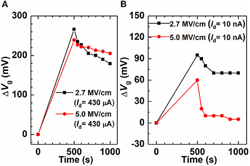
Figure 6. Time-dependence of ΔVg extracted in (A) Id = 430 μA and (B) Id = 10 nA at a constant field strength of E = 2.7 and E = 5.0 MV/cm in stress (0 and 500 s) and recovery (500–1,000 s) phases.
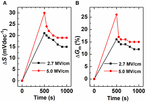
Figure 7. Time-dependence of (A) ΔS and (B) ΔGm in stress (0 and 500 s) and recovery (500–1,000 s) phases.
Extractions of Trap Energy Densities
According to the similar explanation given by Li et al. [29], the distribution curves of border traps were investigated under the stress from ΔVg among the I, S, and R lines. Specifically, (1) donor and acceptor traps are induced at the end of the 500 s stress. (2) Stress-induced donor traps fully recover, while acceptor traps are partially recoverable and partially permanent at the end of 500-s recovery. Although stress-induced acceptor traps are dominant, donor traps may also exist. To distinguish between donor traps and acceptor traps, Δ(Id) represents the density of negatively charged permanent acceptor traps, and Δ(Id) represents recoverable donor traps. Δ(Id)+Δ(Id) or Δ(Id)+Δ(Id) is the total trap, which represents the density difference of negatively charged acceptor traps or positively charged donor traps. Δ(Id)-Δ(Id) is the density of negatively charged recoverable acceptor traps. These parameters can be obtained from:
where Cox is the gate oxide capacitor per unit area and q is the electron charge. We obtain Δ(Vg), Δ(Id), Δ(Id), and Δ(Vg)+ Δ(Vg) as functions of gate bias Vg, as shown in Figures 8A,B. For buried channel InGaAs MOSFETs, the magnitude of total traps is averagely 1.5 × 1012 cm−2 and 1.6 × 1012 cm−2 under medium and high field strengths, respectively, indicating more traps are induced by high field stress than the medium field stress. The medium field stress-induced permanent acceptor trap is calculated to be 1.1 × 1012 cm−2, which is larger than recoverable acceptor trap with the average density of 3.8 × 1011 cm−2. By comparison of the surface channel InGaAs MOSFETs, donor trap is not induced by the medium field stress in the buried InGaAs channel MOSFETs. However, the recoverable acceptor trap and recoverable donor trap are generated by the high field stress with a common density of 8.7 × 1011 cm−2, and the permanent acceptor trap is averagely 7.7 × 1011 cm−2. The results indicate that recoverable trap is easily induced by high field stress. Meanwhile, the medium field stress-induced permanent acceptor trap is larger than the high field stress-induced permanent acceptor trap in the subthreshold region, indicating the permanent acceptor trap and recoverable acceptor trap have been neutralized by recoverable donor trap in the high field stress.
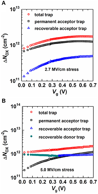
Figure 8. Total trap, permanent acceptor trap, recoverable acceptor trap, and recoverable donor trap area density as a function of gate bias Vg at (A) E = 2.7 and (B) E = 5.0 MV/cm.
Compared to the surface channel InGaAs n-MOSFETs by considering the experimental results of Li et al. [29], the impacts of PBTI stress on buried InGaAs channel n-MOSFETs are summarized as follows: (1) The Dit and ΔNbt distribution of the Al2O3/InP interface is smaller than that of Al2O3/InGaAs interface through the sulfur passivation treatment, indicating the interface reliability of buried InGaAs channel n-MOSFETs are improved by the Al2O3/InP interface. (2) In the surface channel InGaAs n-MOSFETs with the Al2O3/InGaAs interface donor traps become the dominant under the medium field stress. In contrast, the medium field stress-induced the permanent acceptor trap and recoverable acceptor trap are contributed by the degradations of ΔVg and ΔS in the buried InGaAs channel n-MOSFETs with the Al2O3/InP interface, which indicates that the generation of acceptor trap are attributed by the insertion of the InP barrier layer. (3) Compared to the surface InGaAs channel n-MOSFETs under the medium field stress, the acceptor trap become dominant in the subthreshold region for the buried channel one. The buried channel InGaAs MOSFETs is better to maintain the low off-state current developing III-V MOSFETs technology for low-power application.
Conclusions
In summary, the degradation of the buried InGaAs channel n-MOSFETs with an InP barrier layer under PBTI stress and recovery were investigated. The Al2O3/InP interface helps achieve low interface and border traps compared to the Al2O3/InGaAs interface through the sulfur passivation treatment. Contrary to the shift direction of Vg under the medium field stress in the surface InGaAs channel n-MOSFETs, the permanent acceptor trap of 1.1 × 1012 cm−2 and recoverable acceptor trap of 3.8 × 1011 cm−2 become the dominant to produce a positive shift in Vg in the buried InGaAs channel n-MOSFETs. The high field stress-induced recoverable donor trap of 8.7 × 1011 cm−2 cause degradation of ΔS and ΔGm in the subthreshold region, whereas the degradation of Id-Vg is contributed by the recoverable acceptor trap and permanent acceptor trap in the on-state region. Compared to the surface InGaAs channel n-MOSFETs under medium field stress, the low leakage current can be achieved in the buried InGaAs channel n-MOSFETs with an InP barrier layer.
Data Availability Statement
All datasets generated for this study are included in the article/supplementary material.
Author Contributions
HLi was the leader of the work and responsible for the main of experiment and paper writing. KQ, XG, YLi, YC, ZZ, and LM were responsible for single step of the fabrication process. FZ and XZ were responsible for device testing. TF, XL, YLiu, TS, and HLiu were mainly engaged in picture editing and related data processing. TS and HLiu contributed to the modification and suggestion in this paper.
Funding
This work was supported by National Natural Science Foundation of China (Nos. 11965009, 61874036, 61805053, and 61764001), Guangxi Innovation Research Team Project (No. 2018GXNSFGA281004), Guangxi Science and Technology Planning Project (Nos. AD18281030, AD18281084, AD18281034, and AD18281037), Guangxi Natural Science Foundation (Nos. 2016GXNSFDA380021, 2017GXNSFAA198164, 2018GXNSFBA050052, 2018GXNSFBA281152, and 2018GXNSFAA281201), Guangxi Key Laboratory of Precision Navigation Technology and Application (Nos. DH201801, DH201808, DH201702, and DH201701), and Innovation Project of GUET Graduate Education (No. 2018YJCXB15).
Conflict of Interest
The authors declare that the research was conducted in the absence of any commercial or financial relationships that could be construed as a potential conflict of interest.
References
1. Alamo D, Jesus A. Nanometre-scale electronics with III-V compound semiconductors. Nature. (2011) 479:317–23. doi: 10.1038/nature10677
2. Kulbachinskii VA, Yuzeeva NA, Galiev GB, Klimov EA, Vasil'evskii IS, Khabibullin RA, et al. Electron effective masses in an InGaAs quantum well with InAs and GaAs inserts. Semicon Sci Technol. (2012) 27:035021. doi: 10.1088/0268-1242/27/3/035021
3. Selmi L, Caruso E, Carapezzi S, Visciarelli M, Gnani E, Zagni N, et al. Modelling nanoscale n-MOSFETs with III-V compound semiconductor channels: from advanced models for band structures, electrostatics and transport to TCAD. In: IEEE International Electron Devices Meeting (IEDM), San Francisco, CA (2017).
4. Wu H, Ye PD. Fully depleted Ge CMOS devices and logic circuits on Si. IEEE Electron Device Lett. (2016) 63:3028–35. doi: 10.1109/TED.2016.2581203
5. Tewari S, Biswas A, Mallik A. Investigation on high-performance CMOS with p-Ge and n-InGaAs MOSFETs for logic applications. IEEE Trans Nano. (2015) 14:275–81. doi: 10.1109/TNANO.2015.2390295
6. Takagi S, Zhang R, Suh J, Kim SH, Yokoyama M, Nishi K, et al. III-V/Ge channel MOS device technologies in nano CMOS era. J Appl Phys. (2015) 54:06FA01. doi: 10.7567/JJAP.54.06FA01
7. Guo Y, Li H, Robertson J. AlN and Al oxy-nitride gate dielectrics for reliable gate stacks on Ge and InGaAs channels. J Appl Phys. (2016) 119:204101. doi: 10.1063/1.4951004
8. Franco J, Putcha V, Vais A, Sioncke S, Waldron N, Zhou D, et al. Characterization of oxide defects in ingaas mos gate stacks for high-mobility n-Channel MOSFETs. In: IEEE International Electron Devices Meeting (IEDM), San Francisco, CA (2017).
9. Bouzid A, Pasquarello A. Electron trap states at InGaAs/oxide interfaces under inversion through constant Fermi-level abinitio molecular dynamics. J Phys. (2017) 29:505702. doi: 10.1088/1361-648X/aa9a00
10. Mo J, Lind E, Roll G, Wernersson LE. Reduction of off-state drain leakage in InGaAs-based metal-oxide semiconductor field-effect transistors. Appl Phys Lett. (2017) 105:033516. doi: 10.1063/1.4891569
11. He G, Zhu LQ, Sun ZQ, Wan Q, Zhang L. Integrations and challenges of novel high-k gate stacks in advanced CMOS technology. Prog Mater Sci. (2011) 56:475–572. doi: 10.1016/j.pmatsci.2011.01.012
12. Tang K, Droopad R, Mclntyre PC. Bias temperature stress induced hydrogen depassivation from Al2O3/InGaAs interface defects. J Appl Phys. (2018) 123:025708. doi: 10.1063/1.4994393
13. Tang K, Winter R, Zhang LL, Droopad R, Eizenberg M, McIntyre PC. Border trap reduction in Al2O3/InGaAs gate stacks. Appl Phys Lett. (2015) 107:202102. doi: 10.1063/1.4936100
14. Minseok C, Anderson J, Walle CGVD. Native point defects and dangling bonds in α-Al2O3. J Appl Phys. (2013) 113:044501. doi: 10.1063/1.4784114
15. Kwon HM, Kim DH, Kim TW. Relationship between effective mobility and border traps associated with charge trapping in In0.7Ga0.3As MOSFETs with various high-K stacks. Appl Phys Express. (2018) 11:034101. doi: 10.7567/APEX.11.034101
16. Vais A, Franco J, Martens K, Lin D, Sioncke S, Putcha V, et al. A new quality metric for III-V/High-k MOS gate stacks based on the frequency dispersion of accumulation capacitance and the CET. IEEE Electron Device Lett. (2017) 38:318–21. doi: 10.1109/LED.2017.2657794
17. Chang HD, Sun B, Xue BQ, Liu GM, Zhao W, Wang SK, et al. Effect of the Si-doped In0.49Ga0.51P barrier layer on the device performance of In0.4Ga0.6As MOSFETs grown on semi-insulating GaAs substrates. Chin Phys B. (2013) 22:077306. doi: 10.1088/1674-1056/22/7/077306
18. Xue F, Zhao H, Chen YH, Wang Y, Wang Y, Zhou F, et al. High-k InGaAs metal-oxide-semiconductor field-effect-transistors with various barrier layer materials. Appl Phys Lett. (2011) 99:033507. doi: 10.1063/1.3611502
19. Tewari S, Biswas A, Mallik A. Impact of different barrier layers and indium content of the channel on the analog performance of InGaAs MOSFETs. IEEE Trans Electron Dev. (2013) 60:1584–89. doi: 10.1109/TED.2013.2249071
20. Krylov I, Ritter D, Eizenberg M. The role of the substrate on the dispersion in accumulation in III-V compound semiconductor-based metal-oxide-semiconductor gate stacks. Appl Phys Lett. (2015) 107:103503. doi: 10.1063/1.4930202
21. Benbakhti B, Ayubi-Moak JS, Kalna K, Lin D, Hellings G, Brammertz G, et al. Impact of interface state trap density on the performance characteristics of different III–V MOSFET architectures. Microelectron Reliab. (2010) 50:360–64. doi: 10.1016/j.microrel.2009.11.017
22. Deora S, Bersuker G, Loh WY, Veksler D, Matthews K, Kim TW, et al. Positive bias instability and recovery in InGaAs channel nMOSFETs. IEEE Trans Device Mater Reliab. (2013) 13:507–14. doi: 10.1109/TDMR.2013.2284376
23. Wang SK, Sun B, Cao MM, Chang HD, Su YY, Li HO, et al. Modification of Al2O3/InP interfaces using sulfur and nitrogen passivations. J Appl Phys. (2017) 121:184104. doi: 10.1063/1.4982904
24. Haimoto T, Hoshii T, Nakagawa S, Takenaka M, Takagi S. Fabrication and characterization of metal-insulator-semiconductor structures by direct nitridation of InP surfaces. Appl Phys Lett. (2010) 96:012107. doi: 10.1063/1.3269906
25. Hoshii T, Yokoyama M, Yamada H, Hata M, Yasuda T, Takenaka M, et al. Impact of InGaAs surface nitridation on interface properties of InGaAs metal-oxidesemiconductor capacitors using electron cyclotron resonance plasma sputtering SiO2. Appl Phys Lett. (2010) 97:132102. doi: 10.1063/1.3464170
26. Wang SK, Cao MM, Sun B, Li HO, Liu HG. Reducing the interface trap density in Al2O3/InP stacks by low-temperature thermal process. Appl Phys Express. (2015) 8:091201. doi: 10.7567/APEX.8.091201
27. Maeda F, Watanabe Y, Oshima M. Surface chemical bonding of (NH4)2Sx treated InP(001). Appl Phys Lett. (1993) 62:297–99. doi: 10.1063/1.108996
28. Jin HS, Cho YJ, Seok TJ, Kim DH, Kim DW, Lee SM, et al. Improved interface properties of atomic-layer-deposited HfO2 film on InP using interface sulfur passivation with H2S pre-deposition annealing. Appl Surf Sci. (2015) 357:2306–12. doi: 10.1016/j.apsusc.2015.09.232
29. Li ML, Jiao G, Hu Y, Xuan Y, Huang D, Ye PD. Reliability of high mobility InGaAs channel n-MOSFETs under BTI Stress. IEEE Trans Dev Mater Reliab. (2013) 13:515–23. doi: 10.1109/TDMR.2013.2276075
30. Shen C, Li MF, Wang XP, Yeo YC, Kwong DLA. Fast measurement technique of MOSFET Id–Vg characteristics. IEEE Electron Device Lett. (2006) 27:55–7. doi: 10.1109/LED.2005.861025
31. Castagne R, Vapaille A. Apparent interface state density introduced by the spatial fluctuations of surface potential in an MOS structure. Electron Lett. (1970) 6:691. doi: 10.1049/el:19700481
32. Jiao GF, Yao CJ, Xuan Y, Huang DM, Ye PD, Li MF. Experimental investigation of border trap generation in InGaAs nMOSFETs with Al2O3 gate dielectric under PBTI stress. IEEE Trans Electron Dev. (2012) 6:1661. doi: 10.1109/TED.2012.2190417
Keywords: PBTI, Al2O3/InP interface, InGaAs MOSFET, border trap, buried channel
Citation: Li H, Qu K, Gao X, Li Y, Chen Y, Zhou Z, Ma L, Zhang F, Zhang X, Fu T, Liu X, Liu Y, Sun T and Liu H (2020) Reliability of Buried InGaAs Channel n-MOSFETs With an InP Barrier Layer and Al2O3 Dielectric Under Positive Bias Temperature Instability Stress. Front. Phys. 8:51. doi: 10.3389/fphy.2020.00051
Received: 21 December 2019; Accepted: 20 February 2020;
Published: 06 March 2020.
Edited by:
Lin Chen, University of Shanghai for Science and Technology, ChinaCopyright © 2020 Li, Qu, Gao, Li, Chen, Zhou, Ma, Zhang, Zhang, Fu, Liu, Liu, Sun and Liu. This is an open-access article distributed under the terms of the Creative Commons Attribution License (CC BY). The use, distribution or reproduction in other forums is permitted, provided the original author(s) and the copyright owner(s) are credited and that the original publication in this journal is cited, in accordance with accepted academic practice. No use, distribution or reproduction is permitted which does not comply with these terms.
*Correspondence: Tangyou Sun, suntangyou@guet.edu.cn; Honggang Liu, liuhonggang@ime.ac.cn