Investigation of laser-induced contamination on dielectric thin films in MHz sub-ps regime
 Marek Stehlik1 Janis Zideluns1 Camille Petite1 Valentin Allard1 Marco Minissale2 Antonin Moreau1
  Aude Lereu1 Fabien Lemarchand1 Frank Wagner1 Julien Lumeau1
  Laurent Gallais1*
- 1Aix Marseille Univ, CNRS, Centrale Med, Institut Fresnel, Marseille, France
- 2Aix Marseille Univ, CNRS, PIIM, Marseille, France
High-repetition rate diode-pumped sub-ps lasers are widely used in the industrial sector for high-quality material processing applications. However, for their reliable operation, it is crucial to study the power handling capabilities of the optical components used in these systems. The optical components, such as mirrors, gratings, dichroic filters, and gain media, are designed based on dielectric thin films. When subjected to high-intensity laser radiation, the phenomenon of laser-induced contamination (LIC) can lead to the growth of a nanometric, highly absorbent layer on an irradiated optical surface, which can result in transmission or reflection loss and eventual permanent damage. In this study, we investigate LIC growth on dielectric oxide thin films in an air environment irradiated by MHz sub-ps laser at 515 nm. We examine the effect of thin film deposition method, material, and thickness on LIC growth dynamics. The irradiated spots on the surface are inspected using multiple observation methods, including white light interference microscopy and fluorescence imaging. Our results show that the LIC growth dynamics depend on the laser intensity and irradiation time and can be affected by the thin film deposition method, material, and thickness. These findings could be used to inform the development of more resistant optical components, ensuring long-term reliable laser operation required for industrial applications. The study highlights the need for validating optical components using tests that closely mimic real-world applications and provides insight into the complex processes that lead to LIC.
1 Introduction
High-repetition rate diode-pumped sub-ps lasers have become essential tools for precise and high-quality material processing applications, including cutting, drilling, welding, and marking in the industrial sector (Graf and Neunschwander, 2018; Abdou Ahmed et al., 2021; Audouard et al., 2021; Eidam et al., 2021; Wang et al., 2021). To ensure the reliable operation of these systems, the power handling capabilities of the optical components used in them need to be carefully studied. These components, such as mirrors, gratings, dichroic filters, or gain media, often have dielectric thin films as the basis for their designs.
When subjected to high-intensity laser radiation, dielectric thin films can suffer from nonlinear ionization processes that lead to damage onset. Additionally, in the multiple pulse regime, laser-induced defects can be generated, which facilitate the ionization process by making new energy levels within the bandgap electronic structure accessible (Mero et al., 2005; Douti et al., 2014). If the laser pulses are emitted at high repetition rates, the dielectrics can experience heat accumulation, causing stress or failure (Eaton et al., 2005; Nagy et al., 2015; Finger et al., 2018). The damage resistance of components in high-repetition-rate lasers is also related to the damage growth process initiated by localized defects (Cheng and Wang, 2014; Negres et al., 2016; Sozet et al., 2017; Hao et al., 2018; Velpula et al., 2019). Due to the complexities of the processes that lead to laser damage, it is critical to validate optical components using tests that are as close to the applications as possible.
Interestingly, even when components exhibit high laser-induced damage threshold (LIDT) fluence, their long-term reliability may be restricted to fluences much lower than the LIDT value (Abdeldayem et al., 2005). This reduction in reliable laser operation lifetime is linked to a detrimental phenomenon known as laser-induced contamination (LIC) (Hovis et al., 1995; El Reaidy and Gallais, 2020). The LIC process refers to the growth of a nanometric layer on an irradiated optical surface, see Figure 1. LIC is the result of the interaction between the laser beam, the optical surface, and compounds in the surrounding environment. A contamination layer is typically created by organic compounds or other molecules on optical components that undergo photopolymerization due to laser irradiation (Scurlock, 2005; Wernham et al., 2010; Otto, 2015). Irradiation of the contamination-based layer causes chemical reactions yielding a loss of volatility of the contaminants. A thin LIC deposit is thus formed under the beam, which modifies the optical component properties. The LIC process can lead to deterioration of optical component properties, resulting in transmission loss (for optics with antireflective coating) or reflection (for optics with reflective coating) and possibly permanent damage on the optics surface (Schröder et al., 2013). The contamination-based layer may cause irreversible damage to the optics surface (e.g., microcracks), leading to laser failure (Hovis et al., 1995; Kokkinos et al., 2017).
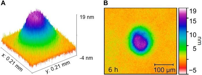
FIGURE 1. LIC deposit detected ex-situ by optical profilometry on SiO2 layer of 450 nm thickness. (A): 3D surface topography; (B): 2D surface topography. Both images show the same LIC deposit obtained after 6 h of irradiation with 700-fs 515-nm 3-MHz laser emitting 35-W of mean power, 10-µJ pulse energy. The near Gaussian laser beam profile had a 1/e2 diameter of 130 µm.
The LIC formation leading to optical damage in sealed laser systems was first documented in 1994 (Hovis et al., 1994), but it is still a serious concern in today’s high-performance laser systems (Zhang et al., 2017; Hubka et al., 2021). The LIC effect has mostly been explored in the context of space applications (Chen et al., 2006; Schröder et al., 2017), where it has been proven to cause unreliable and short-term operation of nanosecond UV lasers used in space flight missions (Abdeldayem et al., 2005; Riede et al., 2011; Kokkinos et al., 2015). In some studies, it has been demonstrated that coating optics with fluorinated films is a potential strategy for preventing the formation of an organic contamination layer (Weiller et al., 2012).
For the fs/ps pulse duration regime, the LIC has been observed on gratings irradiated in a vacuum by a beam with a wavelength of 1,030 nm (Hubka et al., 2021). It has been found that the contaminated surface of the gratings can be cleaned using a radio frequency plasma source, whose regular application can ensure the reliable operation of the laser source. In the same work, LIC was also observed at 515 nm. Usually, the effect is enhanced with higher photon energy. Although LIC proved to be critical for lasers operating in a vacuum and identified as a major risk for the use of lasers in space, it has been discovered that LIC also occurs in high-power lasers operating in air (Möller et al., 2007). Recently, a study on dielectric mirrors irradiated by sub-ps pulses at MHz repetition rates revealed LIC formation in an air environment (El Reaidy and Gallais, 2020). Therefore, the study of LIC formation is of paramount importance for MHz laser applications that operate in air environment.
In this work, we investigate LIC growth on dielectric oxide thin films in air environment irradiated by MHz sub-ps laser at 515 nm. The experiments were performed in similar conditions as in the work (El Reaidy and Gallais, 2020). We study the effect of thin film deposition method, thin film material and thin film thickness on LIC growth dynamics. We observe the LIC growth dynamics in dependence of laser intensity and irradiation time. The irradiated spots on surface are inspected via multiple observation methods covering white light interference microscopy and fluorescence detection. Such detailed investigation is necessary to develop new designs of optical components that will be more resistant to LIC formation. The optical components could ensure long-term reliable laser operation required for industrial applications.
Overall, the LIC phenomenon has been observed to have significant implications for the long-term reliability of high-repetition rate sub-ps laser systems in air environments. Given the importance of these systems in various industrial applications, it is crucial to better understand the underlying mechanisms of LIC formation and develop strategies to mitigate its detrimental effects. Through our experiments on dielectric oxide thin films, we aim to contribute to the growing body of research on LIC and provide insights that can inform the design of more robust optical components for industrial laser systems.
2 Samples
The samples tested for LIC growth were dielectric oxide single layer coatings whose parameters are listed in Table 1. We tested SiO2, HfO2 and Nb2O5 single layers on fused silica substrates. The SiO2 coatings were deposited by plasma assisted reactive magnetron sputtering (PARMS) and plasma-ion assisted deposition (PIAD). In the case of HfO2, the fabrication methods were PARMS, PIAD and ion-beam sputtering (IBS). The Nb2O5 coatings were made only by PARMS. These technologies produce dense and smooth coatings with roughness similar to the substrate one (high quality fused silica substrates).
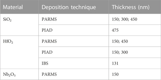
TABLE 1. Single-layer coating materials intended for laser-induced contamination tests. The coatings produced by plasma assisted magnetron-sputtering (PARMS), by plasma-ion assistance deposition (PIAD) and by Ion-Beam Sputtering (IBS).
The LIC tests are performed on coatings with thicknesses ranging from 131 nm up to 475 nm. Except an IBS layer coated on 6 mm thick fused silica and a 150 µm thin substrate of a sample dedicated for ex-situ XPS analysis, the substrate was 2 mm thick fused silica. The coatings were deposited at Institut Fresnel, with the exception of IBS HfO2 coating produced by Laboratoire Matériaux Avancés (Villeurbanne, France).
3 LIC experiments and methodology
A variety of experimental setups are available in the scientific community for conducting Laser-Induced Contamination tests. Some setups, including those described in references (Hovis et al., 1996; Chen et al., 2006; Leinhos et al., 2010; Riede et al., 2011; Balasa et al., 2014; Kokkinos et al., 2015; El Reaidy et al., 2018), have been used to test optics intended for space applications, with a focus on studying contamination growth in the nanosecond UV regime. To simulate space conditions, a high vacuum chamber is utilized, and contamination growth is regulated by introducing a selected contaminant into the chamber. Studies on molecular contamination under nanosecond UV laser irradiation have also been undertaken in high-power laser facilities specialized in fusion research, such as those described in references (Bien-Aimé et al., 2009; Cheng et al., 2014; Favrat et al., 2014; Field and Kletecka, 2019). However, the highly powerful pulses emitted by these facilities have a very low repetition rate, which limits the total number of laser pulses used in experiments.
Different diagnostic methods have been used to study surface modifications and contamination growth. In situ techniques include measurements of transmission loss (Kokkinos et al., 2015) and laser-induced fluorescence (Schröder et al., 2007). Ex-situ diagnostics relevant to contamination investigation include differential interference contrast microscopy, confocal fluorescence microscopy, optical profilometry, and atomic force microscopy (AFM) (El Reaidy et al., 2018).
In light of these facts, we designed a laser damage testing station that enables in-situ sample monitoring as well as real-time transmission loss measurements and possible thermal monitoring with infrared thermography. Since many high-repetition rate industrial laser systems operate in an ambient air environment, we used our experimental station for LIC tests in air. However, we did not control the air properties (water content, pressure, temperature) in our study. Additionally, we used ex-situ techniques such as optical profilometry, fluorescence microscopy, X-ray photoelectron spectroscopy, atomic force microscopy, and absorption measurements to analyze the laser-induced contamination deposits.
3.1 Experimental set-up
The LIC tests were conducted using a high-power industrial laser source (EOLITE Chinook) that generates pulses at a repetition rate of 3.3 MHz with a duration of 700 fs at a wavelength of 515 nm. The average power of the laser was approximately 35 W, which corresponds to a pulse energy of 10 μJ. The laser pulses were reflected by three mirrors, as shown in the schematic drawing in Figure 2, and directed towards a fused silica planoconvex lens with a focal length of 20 cm.
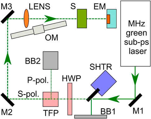
FIGURE 2. Experimental setup with sub-ps green high-repetition rate laser source used for LIC tests. S - tested sample, MX - x-th mirror, SHTR - shutter, BBX - x-th beam blocker, OM - optical microscope (Zoom VZM 450 Edmund Optics), HWP - half-wave plate, TFP - UVFS thin film polarizer (transmission of S vertical polarization 99%, reflection of P horizontal polarization 99.5%, 420-1244E Eksma Optics), EM - energy meter.
The lens was moved along a motorized linear stage to adjust the beam size on the front side of the sample and to achieve the suitable fluence (slightly lower than the LIDT value) for the LIC tests. By moving the lens, we were able to reduce the fluence on the sample while maintaining the full power of the laser source. Therefore, no power reduction through a combination of half-wave plate (HWP) and thin-film polarizer (TFP) was used. The combination of these elements was solely used for power reduction in the laser damage tests performed to determine the position of the focal plane.
During the LIC tests, the average power transmitted through a sample was recorded by a calorimeter (EM, Ophir L50(150)A-BB-35) to detect possible decreases in transmission caused by contamination or damage. We determined the three standard deviations (3σ) of pulse energy stability to be 1.3%. The irradiation of a sample was carried out with linear polarization at an incidence angle close to normal (<5°). The slight inclination from normal incidence was used to protect the lens from heating caused by the reflected beam that was directed to an additional beam blocker.
The LIC tests were performed for lens-sample distances longer than the focal length, which implies that the LIC tests were done with a diverging beam incident on the sample front side plane, where the effective beam diameter was approximately 130 μm. This was done to decrease the experimental fluence on the sample and to avoid damage inside or at the rear side of the sample and to obtain larger LIC deposits.
Throughout the LIC tests, we monitored the state of the tested sample’s front side using imaging optics with a long working distance objective and a CMOS camera. The imaging optics were protected from the bright scattered green laser light by a notch filter. For more sensitive observation, the front side of the sample was illuminated by a fiber halogen lamp.
The thicknesses of contamination deposits were measured ex-situ by optical profilometry (Zygo NewView). Examples of deposits observed by this method are shown in Figure 1.
3.2 Beam profile measurements
The beam profile was measured with high-resolution BeamPro 8.7 camera (FemtoEasy) for tens of lens positions near focal length as can be seen in Figure 3. The camera sensor of 3.45 µm pixel length was placed instead of holder with sample (S), see Figure 2, in normal incidence to the beam. The beam incident to the tested sample had profile close to Gaussian one with M2 of approximately 1.3.
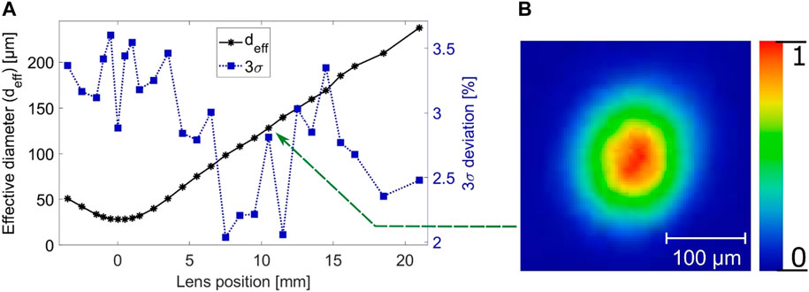
FIGURE 3. Beam profile of MHz sub-ps green laser measured with a sensor of 3.45 µm pixel length: (A) effective beam diameter (deff) and 3σ standard deviation of effective area as a function of lens position. The 0 position is at the focal plane; (B) beam profile corresponding approximately to the lens position used for LIC tests with effective beam diameter around 130 µm. For lens positions >0, the CMOS sensor of the beam profiler is farther from the lens than the focal plane.
To avoid high laser light exposure to the CMOS sensor, the beam profiling was carried out in low power mode (2.1 MHz repetition rate, 130 mW). Furthermore, the pulse energy was reduced by using a neutral density filter (ND3-4) and a combination of half-wave plate (HWP) and thin-film polarizer (TFP). We applied a minimum exposure time of 39 μs, which corresponds to approximately 82 pulses and 44 frames per second.
For each lens position, we recorded 100 frames. The effective beam areas were analyzed using the maximum exposure value detected on a single pixel, without using any averaging method. The dependence of the effective beam diameter on the lens position is shown in Figure 3, with the beam profile corresponding to the one used for the LIC tests. At the focal plane, the effective beam diameter was approximately 30 μm, whereas the diameter used for the LIC tests was around 130 μm. We found values of the 3 standard deviations of beam area reaching up to 3.5% (Figure 3A).
3.3 Test procedure
The LIC tests with the coated samples were conducted using the full laser power of approximately 35W, with a wide range of durations ranging from 2 s up to 6 h. The irradiation of a tested sample was terminated if damage of the film was detected with the in-situ microscope, to avoid contamination by surface debris, or at the end of the intended irradiation time for further ex-situ analysis. After the irradiation of a given spot on the sample was completed, the next test was performed at a sufficient distance from the previous one to prevent any laser-induced surface modifications before the given test. The typical distance between the irradiated spots was 1mm, and the effective beam diameter was approximately 130 μm.
3.4 Error contributors
The uncertainty in LIC thickness measurement via optical profilometry is estimated to be approximately ±1 nm. Another source of uncertainty is related to focal plane determination. Due to the chosen step in lens positions and sensitivity of the in-situ imaging system, we assume an uncertainty in focal plane determination of approximately ±0.5 mm. This causes an uncertainty in the effective beam areas and, consequently, an uncertainty in the irradiance values used for LIC testing of about 10%. Therefore, we consider this error contributor to be significantly larger than the pulse-to-pulse variations of beam sizes or pulse energies. Despite these uncertainties, our comparison of results between the LIC campaigns (Figure 4) indicates good experimental reproducibility.1 This is valid for both the initial growth rate of the LIC deposit and the maximum height at which it saturates.
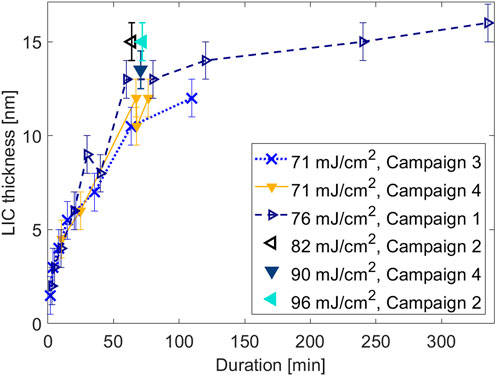
FIGURE 4. LIC deposit thicknesses on 450 nm thick PARMS SiO2 coating show good experimental reproducibility across four LIC test campaigns. The legend shows experimental fluences. The LIC deposit thicknesses correspond to the maxima found on spot areas analyzed using the optical profilometer. The lines connecting datapoints from the same dataset are shown only as a guide for eye.
The comparison of LIC deposit growth dynamics between four campaigns was done for 450 nm thick SiO2 coatings produced by magnetron-sputtering in the same deposition batch. The results suggest a trend: a slight increase in the irradiance of the coating tends to result in a modest increase in the LIC deposit thickness. This generalization is valid assuming that the uncertainty of the LIC thickness measurement by the used optical profiler is approximately ±1 nm.
4 Parametric study of laser-induced contamination on single layer coatings
The aim of this study was to investigate the dynamics of LIC growth and the dependence of LIC deposit thickness on test duration. We were able to study the LIC growth dynamics as a function of coating material, deposition method, and thickness thanks to the access to numerous samples, whose parameters are listed in Table 1. The LIC deposit thicknesses presented in this section correspond to the maxima found on spot areas analyzed using the optical profilometer. In the majority of LIC tests, we used experimental fluences between 70 and 80 mJ/cm2, which is 1-2 orders of magnitude lower than the LIDTs of dielectric coating single layers determined with a 500 fs, 1,030 nm, 10 Hz setup. The corresponding values of the mean and peak intensities used in the tests are listed in Table 2.
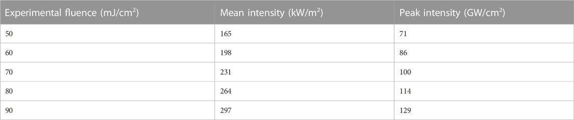
TABLE 2. Conversion between physical quantities. Majority of LIC tests was done with experimental fluences between 70 and 80 mJ/cm2.
4.1 Effect of material
Figure 5 presents the results obtained for three magnetron-sputtered coating materials, SiO2, HfO2, and Nb2O5, within the same LIC test campaign. At an experimental fluence of 76 mJ/cm2, only SiO2 coatings showed clear LIC deposits thicker than 2 nm. For HfO2 samples, we either did not detect any surface modification or observed catastrophic damage. Even after 6 h of irradiation using a fluence of 60 mJ/cm2, we did not observe any LIC deposit on 150 nm thick HfO2. Nb2O5 was also challenging to study, as it is susceptible to damage under the conditions used. Nevertheless, we found 2 nm thick LIC deposits in two cases.
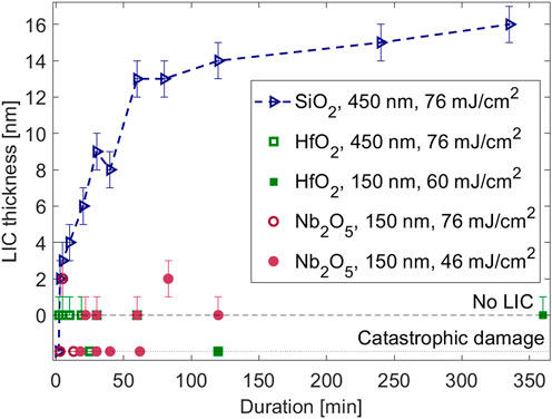
FIGURE 5. Effect of material on LIC dynamics. All results refer to samples deposited by magnetron sputtering and tested in the same LIC campaign. On some samples damage occurred during the exposition, and the LIC thickness was consequently dot determined (referred to as a negative value on the graph). On the irradiated sites of HfO2, we did not detect any contamination deposit. In the case of Nb2O5, the growth of contamination layers thicker than 2 nm was not possible, since the irradiation conditions were close to damage threshold at 3.3 MHz repetition rate. The dashed line connecting SiO2 LIC thicknesses is shown only as a guide for eye.
Focusing on the LIC deposit growth dynamics on SiO2 coatings, we can distinguish between the growth phase and the saturation period. We detected a 2 nm thick LIC deposit after only 3 min of irradiation, and 3 nm after 5 min. The thickness of the LIC deposit increased to 4 nm after 10 min and to 6 nm after 20 min of irradiation. These results suggest that the LIC thickness growth rate is highest at the beginning of irradiation, with a rate of up to 1 nm per minute, and gradually decreases. After 60 min of irradiation, the rate of LIC deposit thickness growth noticeably decreases to approximately 1 nm per hour, and the deposit thickness saturates.
4.2 Effect of thickness
The effect of coating thickness on LIC growth dynamics was investigated using magnetron-sputtered SiO2 coatings and HfO2 produced by PIAD. Results for SiO2 coatings with thicknesses of 150, 300, and 450 nm are shown in Figure 6. The results demonstrate a correlation between coating thickness and LIC deposit thickness, indicating approximately linear dependence of the final (saturated) LIC deposit thickness and the initial growth rate on the coating thickness.
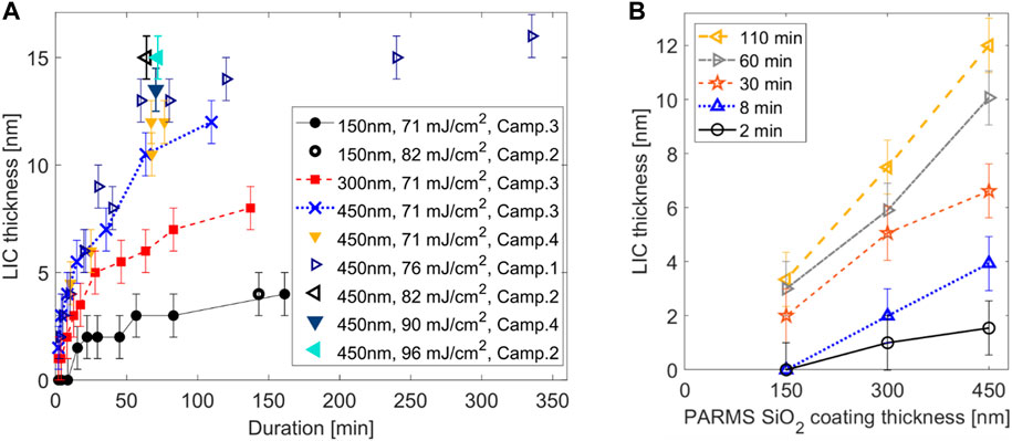
FIGURE 6. Effect of PARMS SiO2 coating thickness on LIC growth dynamics: (A) LIC thickness measured across 4 campaigns for 3 coating thicknesses of 150 nm, 300 nm and 450 nm; (B) LIC thickness as a function of coating thickness. The data points in Panel (B) were obtained by linear interpolation from the datasets corresponding to the Campaign 3. Comparison of the data from the same campaign ensures the same experimental conditions – the same sample positioning and the experimental fluence (71 J/cm2). The lines connecting data points from the same dataset are shown only as a guide for eye. In the Panel (A), the lines correspond to datasets from the Campaign 3.
The impact of coating thickness on LIC deposit growth dynamics was also investigated with PIAD-deposited HfO2 single layers, and the results for detected LIC deposits on 150 nm and 300 nm thick HfO2 single layers are plotted in Figure 7. For 150 nm thick PIAD HfO2, we found LIC deposit thickness saturation at around 4 nm after approximately 20 min of irradiation. In the case of 300 nm thick PIAD HfO2, saturation occurred after approximately 20 min, with LIC deposits around 7 nm thick. Assuming an uncertainty of ±1 nm in the LIC thickness measurement, the hypothesis of linear dependence of saturated LIC deposit thickness on coating thickness is still valid. The PIAD SiO2 coating was the thickest coating (475 nm) and showed thicker LIC deposits (up to 13 nm) than those detected on HfO2.
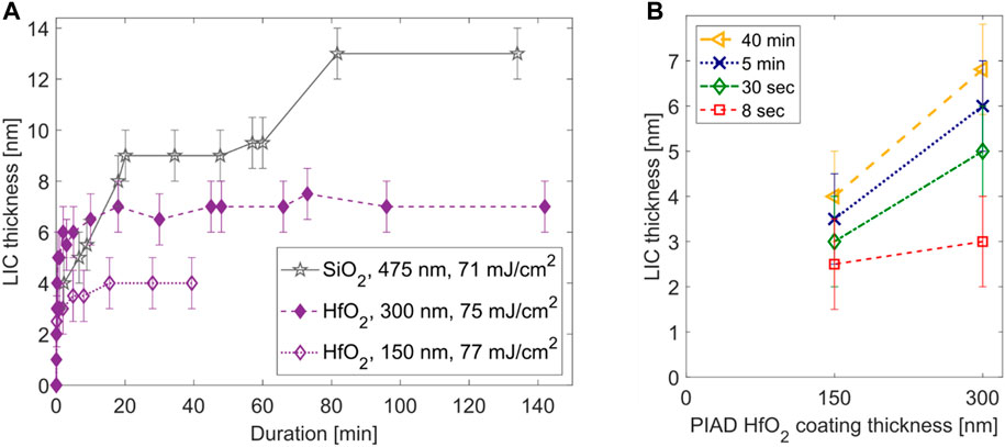
FIGURE 7. Effect of PIAD material and HfO2 coating thickness on LIC growth: (A) LIC thickness in dependence on irradiation duration; (B) LIC thickness as a function of PIAD HfO2 coating thickness. The data points in Panel (B) were obtained by linear interpolation from the datasets for two PIAD HfO2 coatings shown in Panel (A). The lines connecting data points from the same dataset are shown only as a guide for eye.
Comparing the LIC deposit growth dynamics with PARMS SiO2 (Figure 6) and PIAD coatings (Figure 7), the growth in the early phase of irradiation appears to be much faster on PIAD coatings. For example, in the case of 300 nm thick PIAD HfO2, we detected a LIC deposit of 3 nm thickness after only 8 s of irradiation, and 5 nm after 30 s.
4.3 Effect of deposition method
We compared the growth dynamics of LIC across different deposition methods for SiO2 and HfO2 coatings. The comparison of LIC thicknesses between PARMS and PIAD deposited SiO2 coatings of similar thicknesses (PIAD 475 nm, MS 450 nm) is shown in Figure 8. The main difference in dynamics is at the earliest phase of irradiation, where the PIAD coating showed a 4 nm thick deposit after a 2 min long LIC test, while it was only 1.5 nm for the PARMS coating. Therefore, PIAD SiO2 shows faster growth than PARMS SiO2 coating in the first 40 min of irradiation. For LIC test durations longer than 40 min, the difference in LIC deposit thicknesses between the samples is not significant.
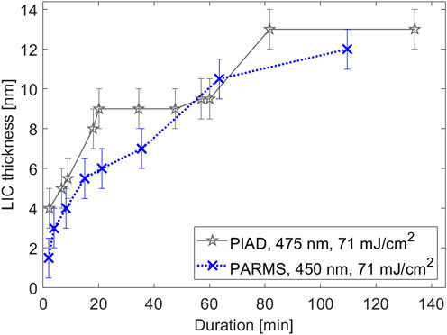
FIGURE 8. Effect of deposition method on LIC growth on SiO2 coatings, which were produced by plasma-ion assistance deposition (PIAD) or by magnetron sputtering (PARMS).
In the case of HfO2, we compared the material responses to laser irradiation of PARMS, PIAD, and IBS deposited coatings, as shown in Figure 9. We found no LIC deposits on the irradiated spots of PARMS and IBS coated HfO2 even after 6 h long tests. At the same time, we observed that these coatings are susceptible to catastrophic damage formation when irradiated at a fluence of 76 mJ/cm2. In the case of PARMS HfO2, a catastrophic damage was observed even at 60 mJ/cm2. The only deposition method that allowed the observations of contamination growth dynamics on HfO2 coating was the PIAD method.
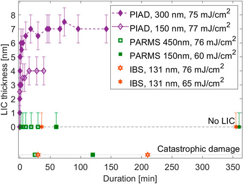
FIGURE 9. Effect of HfO2 deposition method and coating thickness on LIC growth.
From this parametric study it appears that the LIC strongly depends on the coating material, silica being more prone to induce contamination compared to hafnia, independently of the deposition technique. Additionally, the coating thickness directly drives the dynamic of LIC growth suggesting that the coating itself acts as a reservoir for the contamination.
5 Analysis of LIC deposits
In this section, we summarize the results obtained from different characterization techniques: fluorescence, X-ray photoelectron spectroscopy, and scattering-type scanning near-field optical microscopy. We used these methods to analyze LIC deposits on thin-film coatings to gather comprehensive information about their topography, chemical composition, and optical properties. By doing so, we aimed to gain a deeper understanding of LIC and its behavior.
5.1 Fluorescence
To gain insights into the composition of the contamination layer, we investigated some of the irradiated spots using ex-situ fluorescence confocal microscopy. The contamination layer may produce a photoluminescence signal that could aid in determining its chemical composition. We acquired fluorescence images to detect differences in the chemical composition of the LIC deposits obtained for varying irradiation times. To perform these measurements, we used a confocal microscope (Leica TCS SPE) with an excitation wavelength of 405 nm and a detection range from 455 to 800 nm.
Figure 10 shows 2D images of spots on a 450 nm thick PARMS SiO2 coating. The fluorescence images reveal spots that were tested for LIC growth by exposing them to green laser light for periods ranging from 20 min to 4 h.
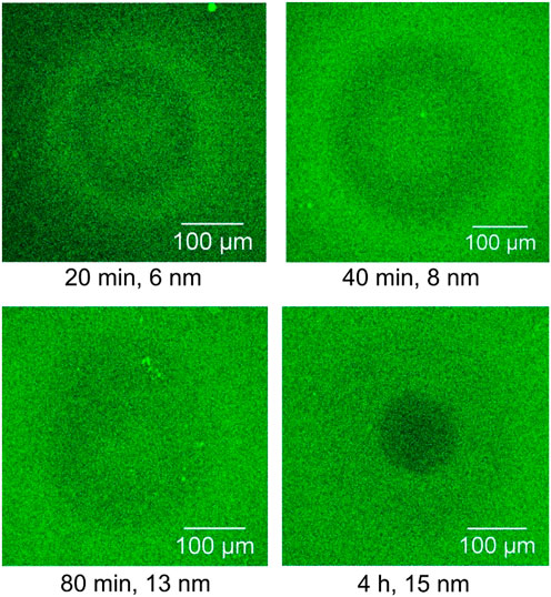
FIGURE 10. Spots on PARMS SiO2 coating of 450 nm thickness observed by ex-situ confocal fluorescence microscope (Leica TCS SPE). Excitation wavelength was 405 nm. Images were captured using ×10 objective magnification with the light spectrum ranging from 455 to 800 nm, with the same acquisition parameters. The labels below the images indicate the exposure duration and LIC deposit thickness determined by the optical profilometer. The fluence for exposition was 76 mJ/cm2.
The evolution of changes in the irradiated spot images suggests that the chemical nature of deposits is modified with irradiation time. Initially, we observed the growth of the deposited area up to 80 min, followed by a second transformation of the deposit that further reduced the fluorescence yield. Similar material transformations were reported for UV nanosecond pulses in a vacuum. (El Reaidy et al., 2018). However, the luminescence signal is weak compared to the background and does not allow a spectral analysis that could give some insight on their composition.
A possible reason for the darker central region observed in the 4-h test could be that the contamination layer absorbed some of the fluorescent or excitation light. Another hypothesis is that the LIC deposit may act as an interferential layer. This effect was previously described in detail in by Wagner et al. (2020), who found that the effective refractive index of LIC deposits can be lower than that of the fused silica substrate due to its nanometric porosity. Such a layer exhibits slightly antireflective characteristics, which was observed during the early phase of the LIC deposit evolution.
Another possibility would be a decrease of the fluorescence yield of the coating material. More investigations are required to understand this effect.
5.2 X-ray photoelectron spectroscopy
To determine the origin of the LIC deposit, knowledge of its chemical composition is essential. X-ray photoelectron spectroscopy (XPS) can identify the elements present in the top few atomic layers (up to 10 nm) of a material’s surface by measuring the kinetic energy of photoelectrons emitted when a material is irradiated with soft x-ray radiation in vacuum. XPS is a quantitative spectroscopic technique that can determine the chemical state, in addition to the elemental composition. It is a surface-sensitive technique that can identify the chemical bonding and composition of a material’s surface.
Due to size constraints of the XPS apparatus, measurements are limited to 1x1 cm2 samples, therefore we did not analyze the same samples used in the parametric study of LIC, but instead used a dedicated sample. A 450 nm thick SiO2 layer was deposited on a 150 μm thin silica substrate by PIAD method to increase the sensitivity of XPS measurements since it results in the thickest LIC deposit (section 3). We analyzed LIC deposits by generating several identical deposits using laser irradiation: we created an array of 5x5 spots on the SiO2 coating, in order to cover a significant surface under the 1 mm2 of XPS measurement area. Each laser irradiation lasted 30 min and resulted in LIC deposit thicknesses of approximately 8 nm, but not yet in the saturation zone. The sample was then laser cut from 1-inch diameter to a size smaller than 1 cm2. XPS spectra were measured by using a non-monochromatized Mg Kα line (hν =1,253.6 eV). The emitted photoelectrons were counted using an R3000 analyzer equipped with a microchannel plate detector. We did not use any neutralizer to compensate possible sample charging.
XPS measurements were performed on both LIC and non-LIC zones on the SiO2 sample. The spectra reported on Figure 11) of the examined zones were similar, with silicon, carbon, oxygen. One can note that, being SiO2 an insulator, all photoemission peaks are shifted towards higher binding energy (around 9.5 eV) due to the negative charges (i.e., photoelectrons) pauperization of the sample. Moreover, we can note the significant presence of carbon: the contamination is present on the entire surface of the sample beyond the LIC zone. The main difference in spectral characteristics between the two zones was the slightly higher carbon peak in the irradiated zone (Figure 11B). This suggests that the LIC deposit is composed of same material as the one on the pristine surface, although additional studies probing the vibrational modes of adsorbed species are needed to understand the nature of species.
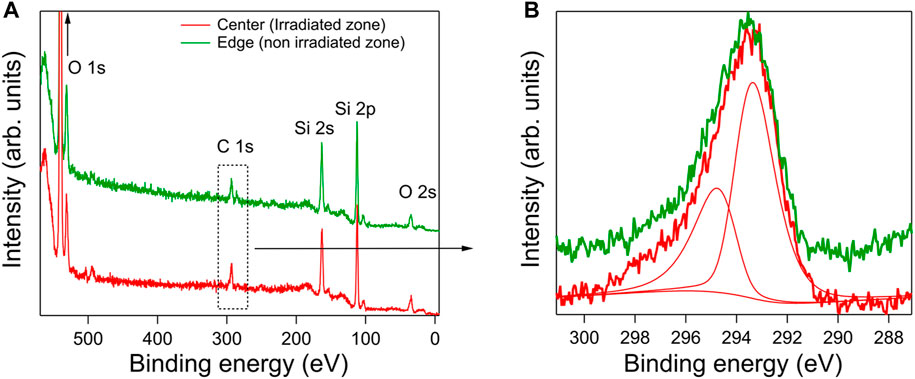
FIGURE 11. (A) Comparison of spectra between the two analyzed zones on SiO2 sample: center part with array of LIC deposits (red) and edge of sample which was not irradiated by the laser. This XPS analysis revealed presence of Si, O, and C. The largest difference between the two analyzed zones, detailed in the inset for C, suggests that there may be carbon compounds characteristic to the LIC. (B) Zoom on the C 1s core level region.
5.3 Atomic force microscopy
AFM measurements were carried out after LIC tests in order to analyze the structure deposit. To perform the AFM characterization shown in this paper, we used a commercially available VIS-neaSCOPE. We chose to work in AFM tapping-mode, allowing us to record the topography, the mechanical amplitude and the mechanical phase for each scan. For this study, the same tip was used to characterize two samples; a NanoWorld® Arrow™ NCR probe with a radius of curvature of 20 nm. Scans were made with a definition of 200 × 200 px2 and, depending on the scan, either a 10 × 10 μm2 surface with an integration time of 21 ms per pixel or a 20 × 20 μm2 surface with an integration time of 17 ms per pixel. We report on Figure 12 the results obtained on a LIC deposit on a 450 nm thick SiO2 layer corresponding to 4 h long irradiation with 76 mJ/cm2.
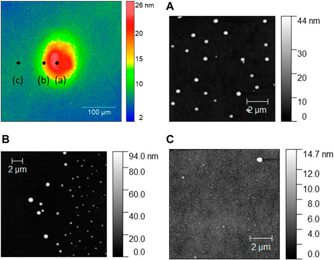
FIGURE 12. Optical Profilometry measurement of a LIC deposit on a 450 nm SiO2 layer obtained after 4 h exposition to 76 mJ/cm2. The different points correspond to the positions of the AFM measurements in 10 × 10 μm2 area. (A) Center of the LIC deposit; (B) edge of the LIC deposit; (C) outside the laser illuminated area.
The AFM measurements reveal a particulate structure, that was not resolved with the optical profilometric measurement. We observed the formation of nanoparticles, resulting from the LIC deposit, in correlation with the deposit thickness measured by optical profilometry. From the topography images in Figure 12, the particles have a diameter in the range of 300- to 400 nm, with an average height of about 50 nm, in the center of the LIC deposit (a), whereas at the edge of the LIC deposit, the diameter spans from 500- to 800 nm, with a height around 100 nm edge (b). We note that, as we move closer to the impact center, the nanoparticles diameter decreases, and their surface density increases.
Furthermore, working in tapping mode using AFM, we can also simultaneously record the mechanical phase of the microcantilever oscillations as in Figure 13 for the different area. A phase lag may be associated to a variation in the viscoelastic properties of the samples. At the center of LIC induced nanoparticles (Figures 13A, B), we observed a phase variation that is not seen over dust particles outside the LIC area (Figure 13C). This let us assumed that the LIC deposit induces some physical and/or chemical changes of the thin film during laser irradiation as mentioned in the introduction. Looking more specifically at the profiles across the LIC induced NP, we observed a larger and more important phase shift (≈0.5 rad) for the NP at the LIC edge that may be correlated to the size and shape of the NPs made on the topography images (Figure 12). This nanostructuration induced by LIC is certainly the cause of the observed changes on the optical profilometry measurements.
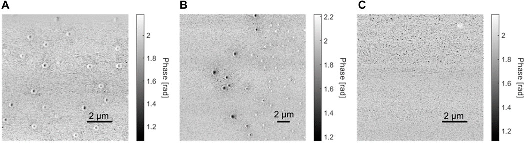
FIGURE 13. Mechanical Phase variation at (A) Center of the LIC deposisit, (B) edge of LIC deposit and (C) outside the laser illuminated area.
6 Discussion
6.1 Thermal effects
The process of Laser Induced Contamination is mainly driven by the local fluence, but thermal energy can also contribute to the growth process of the deposit. This is because the deposited material can be absorbing, causing a temperature rise that can extend far away from the laser spot through heat conduction. Additionally, the fluence not only affects the contaminant deposition rate but can also alter the chemical structure of the deposit, which can further increase the absorption coefficient. For example, Kokkinos et al. (2015) measured a significant temperature rise, above 1000 K, for hydrocarbon contamination induced by ns UV-laser exposure. In similar exposure conditions, Wagner et al. (2020) proposed to explain the lateral growth of LIC deposit by heat conduction from the deposit center to the periphery.
In our irradiation conditions, which have a high repetition rate of 3.3 MHz corresponding to 0.3 µs between each shot, the temperature cannot relax back to the ambient temperature between two pulses. The thermal relaxation time, τr, can be estimated using Eq. 1:
where D is the thermal diffusivity of the material (1 x 10⁻⁶ m2/s for fused silica), and ω is the beam radius incident on the sample. In our case, the beam radius is around 95 µm (at 1/e2), which corresponds to the thermal relaxation time of 2 ms. During high repetition rate irradiation, the temperature should reach a steady-state regime when the losses compensate for the heat coupled in the coating and deposit by laser absorption. In this case, assuming a semi-infinite material with a surface heat source, the temperature attained using a CW laser can be estimated using the following relationship:
where A is the absorption and K is the thermal conductivity (1.38 W/m/K for fused silica). In our test conditions (p = 35 W, ω = 95 µm), the temperature reached in steady state can therefore be evaluated as a function of absorption: ΔT ≈ A x 1.1 x 10⁻⁵°C. For the coatings investigated in this study, the order of magnitude of absorption is 10 ppm (Petite et al., 2022). Therefore, the intrinsic absorption of the coating could lead to an increase in temperature of only 1°C. However, the temperature increase may be higher with non-linear absorption at high intensity (Stenzel et al., 2020). The calculation is a rough approximation, but it shows that no significant temperature increase is expected on the non-contaminated surface. However, the nature of the deposit being unknown at this point, only experimental measurements can be used to evaluate the case of the contaminated surface.
To go further in this investigation, we have implemented an in situ thermographic measurement to experimentally evaluate a possible correlation between temperature increase and LIC growth. We have used a thermal camera (FLIR A655) operating in the Long Wave InfraRed band (8–13 µm) with the emissivity set to 0.85 for the sample under consideration. The camera, thermally calibrated by the manufacturer, was equipped with a macro objective providing a spatial resolution of 100 µm in the imaging configuration.
Experiments were conducted on a magnetron-sputtered 450 nm thick SiO2 coating. The temperature evolution was recorded during 80 min long laser exposure at 3.3 MHz with a mean power of 35W and effective beam diameter of 130 µm. After the exposure, the spot was analyzed ex-situ via the optical profilometer and a LIC deposit thickness of around 12 nm was found. Results are reported in Figure 14.
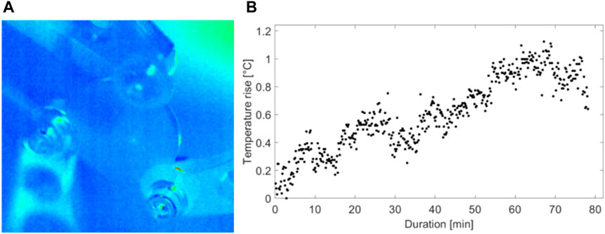
FIGURE 14. Evolution of temperature on 450 nm thick PARMS SiO2 coating during the irradiation inducing LIC: (A) Photograph of irradiated sample captured by thermal camera during the experiment. The heated area is visible at the center of the sample but the temperature rise is less than 1°C compared to the mean temperature of the sample. (B) Temperature rise as a function of duration. Exposure time of the camera was 10 ms and the deposit covered a bit more than one pixel.
The thermal measurements indicate an increase in temperature of only around 1°C, which is in the order of magnitude as the evaluation discuss before. Therefore, these thermal measurements suggest in the one hand that the LIC formation is mainly a cold process, as opposed to pyrolysis process for instance, and in the other hand that the deposit has no significant absorption.
6.2 Nature and formation of the deposit
The main question arising from this work is the nature of the deposit. From the XPS analysis, only C, O and Si elements can be found on the surface, in the exposed and un-exposed area. As shown in the work of Möller et al. (2007), the deposition of an amorphous SiO2 contamination layer on optical surfaces can be activated by UV laser exposure. The process is related to photo-excitation of the reactants (Silicon and oxygen) and photo-excitation of the surface, a deposition mechanism that can be controlled to grow SiO2 films, see for instance Takao et al. (2004). These works were conducted in the case of deep UV light, but in our case the photon energy is lower. However, in our case the surface is exposed to high intensities (see Table 2) and we suggest that the same mechanisms are at play, activated by 2 photon absorption of green light. The fact that there is no laser absorption and temperature increase related to the LIC deposit further support the growth of SiO2, as opposed to hydrocarbons that have been identified as a possible laser-induced deposit in such laser exposure conditions (Hubka et al., 2021) but are efficiently removed in oxidizing environment.
The Si compounds may come from the surrounding environment via outgassing of various Si-based materials, or from the optics under test themselves. The fact that the LIC growth dynamic depends on the coating thickness (Figures 6, 7) may point to the latter. The particulate structure, as revealed by the AFM measurements, is however unclear at this point but may be related to nucleation and growth of SiO2. Nucleation rate and maximum size are closely linked, as observed in UV-induced crystallization (Lumeau et al., 2008). The area exposed to the largest dosage of radiation, the center of the Gaussian beam in our case has large number of tiny particles due to the increase of the nucleation rate associated with the photo-induced process that prevents the growth of large particles. Areas with low exposure, the edge of the Gaussian beam in our case, contain only a few large particles: their small concentration is due to a smaller nucleation rate, hence associated with the growth of large particles, the number is not enough to prevent growth of larger crystals.
7 Conclusion
In this study, we investigated the growth of laser-induced contamination on various classical coating materials used in high power laser optical components, including SiO2, HfO2, and Nb2O5 dielectric coatings, irradiated by 700 fs pulses with a repetition rate of 3.3 MHz in air. Our results indicate that the coating material and deposition method have a significant effect on LIC growth dynamics. We were able to observe LIC deposits on both PARMS and PIAD deposited SiO2 coatings and studied the dependence of LIC deposit thickness on irradiation duration and layer thickness. However, in the case of HfO2 coating, we found LIC deposits only on PIAD deposited samples, while PARMS and IBS HfO2 coatings were susceptible to damage growth. We also observed catastrophic damages on the surfaces of PARMS Nb2O5 coatings, but we did not find LIC deposits thicker than 2 nm.
Our study made several important observations regarding LIC deposit growth. We found a correlation between LIC deposit saturation thickness and coating thickness. This dependence was approximately linear and was observed for PARMS SiO2 and PIAD HfO2 samples. Furthermore, we found that in the early phase of irradiation, the growth rate of LIC deposit on PIAD samples is more dynamic than that of PARMS coatings. For instance, the growth rate on 300 nm thick PIAD HfO2 is 20 times faster than that on 450 nm thick PARMS SiO2.
Thermal measurements performed during the fs laser exposition have evidenced that there is no significant temperature increase during the process, which points toward photo-assisted mechanisms only: photolysis for the dissociation of molecules, creation of free radicals, and photo-fixation of the molecules on the surface. Based on the available literature on the topic, we have suggested that the LIC results from the deposition of an amorphous SiO2 contamination layer, that is activated by 2 photon absorption of green light.
Overall, our study could be useful for further development of design coatings that mitigate LIC growth. However, to fully understand the physics of LIC formation and the composition of the LIC deposit, further characterization of the LIC deposit in situ and ex situ is required.
Data availability statement
The raw data supporting the conclusion of this article will be made available by the authors, without undue reservation.
Author contributions
MS: Conceptualization, Formal Analysis, Investigation, Writing–original draft. JZ: Investigation, Writing–review and editing. CP: Investigation, Writing–review and editing. VA: Investigation, Writing–review and editing. MM: Investigation, Writing–review and editing. AM: Investigation, Writing–review and editing. AL: Supervision, Writing–review and editing. FL: Investigation, Writing–review and editing. FW: Conceptualization, Investigation, Supervision, Writing–review and editing. JL: Funding acquisition, Supervision, Writing–review and editing. LG: Conceptualization, Funding acquisition, Project administration, Supervision, Writing–review and editing, Writing–original draft.
Funding
The author(s) declare financial support was received for the research, authorship, and/or publication of this article. This work has received funding from the European Union’s Horizon 2020 research and innovation programme under the Marie Sklodowska-Curie grant agreement No 813159.
Conflict of interest
The authors declare that the research was conducted in the absence of any commercial or financial relationships that could be construed as a potential conflict of interest.
The author(s) declared that they were an editorial board member of Frontiers, at the time of submission. This had no impact on the peer review process and the final decision.
Publisher’s note
All claims expressed in this article are solely those of the authors and do not necessarily represent those of their affiliated organizations, or those of the publisher, the editors and the reviewers. Any product that may be evaluated in this article, or claim that may be made by its manufacturer, is not guaranteed or endorsed by the publisher.
Footnotes
1The LIC campaigns were conducted over 2 years, during which we recorded a decrease in laser source power of only few percents.
References
Abdeldayem, H. A., Dowdye, E., Canham, J., and Jaeger, T. (2005). Contamination and radiation effects on spaceflight laser systems. SPIE Proc. 5897, 589705. doi:10.1117/12.622345
Abdou Ahmed, M., Roecker, C., Loescher, A., Bienert, F., Holder, D., Weber, R., et al. (2021). High-power ultrafast thin-disk multipass amplifiers for efficient laser-based manufacturing. Adv. Opt. Technol. 10, 285–295. doi:10.1515/aot-2021-0047
Audouard, E., Bonamis, G., Hönninger, C., and Mottay, E. (2021). GHz femtosecond processing with agile high-power laser: high power and flexible fs lasers in GHz burst mode open new horizons for femtosecond laser processing. Adv. Opt. Technol. 10, 263–275. doi:10.1515/aot-2021-0029
Balasa, I., Hippler, M., Schröder, H., Jensen, L., Gauch, M., Ristau, D., et al. (2014). Enhancement of contamination growth and damage by absorption centers under UV irradiation. SPIE Proc. 9237, 92372A. doi:10.1117/12.2085138
Bien-Aimé, K., Belin, C., Gallais, L., Grua, P., Fargin, E., Néauport, J., et al. (2009). Impact of storage induced outgassing organic contamination on laser induced damage of silica optics at 351 nm. Opt. Express 17, 18703–18713. doi:10.1364/OE.17.018703
Chen, P., Hedgeland, R., Ramsey, L., Rivera, R., and Houston, K. (2006). Contamination control of space-based laser instruments. Opt. Syst. Degrad. Contam. Stray Light Eff. Meas. Control II 6291, 629104. doi:10.1117/12.681175
Cheng, X., Miao, X., Wang, H., Qin, L., Ye, Y., He, Q., et al. (2014). Surface contaminant control technologies to improve laser damage resistance of optics. Adv. Condens. Matter Phys. 2014, 1–7. doi:10.1155/2014/974245
Cheng, X., and Wang, Z. (2014). Defect-related properties of optical coatings. Adv. Opt. Technol. 3, 65–90. doi:10.1515/aot-2013-0063
Douti, D. B., Gallais, L., and Commandré, M. (2014). Laser-induced damage of optical thin films submitted to 343, 515, and 1030 nm multiple subpicosecond pulses. Opt. Eng. 53, 122509. doi:10.1117/1.OE.53.12.122509
Eaton, S. M., Zhang, H., Herman, P. R., Yoshino, F., Shah, L., Bovatsek, J., et al. (2005). Heat accumulation effects in femtosecond laser-written waveguides with variable repetition rate. Opt. Express 13, 4708–4716. doi:10.1364/OPEX.13.004708
Eidam, T., Breitkopf, S., Herrfurth, O., Stutzki, F., Kienel, M., Hädrich, S., et al. (2021). High-power ultrafast fiber lasers for materials processing. Adv. Opt. Technol. 10, 277–283. doi:10.1515/aot-2021-0033
El Reaidy, G. G., Wagner, F. R., Faye, D., and Natoli, J. Y. (2018). Study of the first stages of laser-induced contamination. Opt. Eng. 57, 121903. doi:10.1117/1.OE.57.12.121903
Favrat, O., Mangote, B., Tovena-Pécault, I., and Néauport, J. (2014). Study of organic contamination induced by outgassing materials. Application to the Laser MégaJoule optics. Appl. Surf. Sci. 293, 132–137. doi:10.1016/j.apsusc.2013.12.116
Field, E. S., and Kletecka, D. E. (2019). Impact of contamination and aging effects on the long-term laser damage resistance of SiO2/HfO2/TiO2 high reflection coatings for 1054 nm. Opt. Eng. 58, 1. doi:10.1117/1.OE.58.10.105105
Finger, J., Bornschlegel, B., Reininghaus, M., Dohrn, A., Nießen, M., Gillner, A., et al. (2018). Heat input and accumulation for ultrashort pulse processing with high average power. Adv. Opt. Technol. 7, 145–155. doi:10.1515/aot-2018-0008
Gebrayel El Reaidy, G., and Gallais, L. (2020). Analysis of laser-induced contamination at 515 nm in the sub-ps/MHz regime. Opt. Eng. 60, 031004. doi:10.1117/1.OE.60.3.031004
Graf, T., and Neunschwander, B. (2018). The ultrafast laser is gearing up to become a tool for high-precision mass production – opportunities and challenges. Adv. Opt. Technol. 7, 127–128. doi:10.1515/aot-2018-0022
Hao, Y., Sun, M., Guo, Y., Shi, S., Pan, X., Pang, X., et al. (2018). Asymmetrical damage growth of multilayer dielectric gratings induced by picosecond laser pulses. Opt. Express 26, 8791–8804. doi:10.1364/OE.26.008791
Hovis, F. E., Shepherd, B. A., Radcliffe, C. T., Bailey, A. L., and Boswell, W. T. (1994). Optical damage at the part per million level: the role of trace contamination in laser-induced optical damage. Laser-Induced Damage Opt. Mater. 1993 2114. doi:10.1117/12.180872
Hovis, F. E., Shepherd, B. A., Radcliffe, C. T., and Maliborski, H. A. (1995). Mechanisms of contamination-induced optical damage in lasers. SPIE Proc. 2428. doi:10.1117/12.213736
Hovis, F. E., Shepherd, B. A., Radcliffe, C. T., and Maliborski, H. A. (1996). Contamination damage in pulsed 1-μm lasers. 27th Annu. Boulder Damage Symposium Laser-Induced Damage Opt. Mater. 1995 2714, 707–716. doi:10.1117/12.240348
Hubka, Z., Novák, J., Majerová, I., Green, J. T., Velpula, P. K., Boge, R., et al. (2021). Mitigation of laser-induced contamination in vacuum in high-repetition-rate high-peak-power laser systems. Appl. Opt. 60, 533–538. doi:10.1364/AO.414878
Kokkinos, D., Gailly, P., Georges, M. P., Tzeremes, G., Rochus, P., and Fleury-Frenette, K. (2015). Real-time measurement of temperature variation during nanosecond pulsed-laser-induced contamination deposition. Appl. Opt. 54, 10579–10585. doi:10.1364/AO.54.010579
Kokkinos, D., Schroeder, H., Fleury-Frenette, K., Georges, M. P., Riede, W., Tzeremes, G., et al. (2017). Laser optics in space failure risk due to laser induced contamination. CEAS Space J. 9, 153–162. doi:10.1007/s12567-016-0137-1
Leinhos, U., Mann, K., Bayer, A., Dette, J.-O., Schöneck, M., Endemann, M., et al. (2010). Long-term laser induced contamination tests of optical elements under vacuum at 351nm. SPIE Proc. 7842, 78422E. doi:10.1117/12.869297
Lumeau, J., Glebova, L., and Glebov, L. B. (2008). Influence of UV-exposure on the crystallization and optical properties of photo-thermo-refractive glass. J. Non-Crystalline Solids 354, 425–430. doi:10.1016/j.jnoncrysol.2007.06.082
Mero, M., Clapp, B. R., Jasapara, J. C., Rudolph, W. G., Ristau, D., Starke, K., et al. (2005). On the damage behavior of dielectric films when illuminated with multiple femtosecond laser pulses. Opt. Eng. 44, 051107. doi:10.1117/1.1905343
Möller, S., Andresen, Ä., Merschjann, C., Zimmermann, B., Prinz, M., and Imlau, M. (2007). Insight to UV-induced formation of laser damage on LiB_3O_5 optical surfaces during long-term sum-frequency generation. Opt. Express 15, 7351–7356. doi:10.1364/OE.15.007351
Nagy, B. J., Gallais, L., Vámos, L., Oszetzky, D., Rácz, P., and Dombi, P. (2015). Direct comparison of kilohertz- and megahertz-repetition-rate femtosecond damage threshold. Opt. Lett. 40, 2525–2528. doi:10.1364/OL.40.002525
Negres, R. A., Carr, C. W., Laurence, T. A., Stanion, K., Guss, G., Cross, D. A., et al. (2016). Laser-induced damage of intrinsic and extrinsic defects by picosecond pulses on multilayer dielectric coatings for petawatt-class lasers. Opt. Eng. 56, 011008. doi:10.1117/1.OE.56.1.011008
Otto, M. (2015). Airborne molecular contamination: quality criterion for laser and optical components. SPIE Proc. 9346, 93460F. doi:10.1117/12.2076274
Petite, C., Marcouillé, R., Moreau, A., Krol, H., Grèzes-Besset, C., Lumeau, J., et al. (2022). Multipass lock-in thermography for the study of optical coating absorption. Appl. Opt. 61, 978–988. doi:10.1364/AO.445045
Riede, W., Schroeder, H., Bataviciute, G., Wernham, D., Tighe, A., Pettazzi, F., et al. (2011). Laser-induced contamination on space optics. SPIE Proc. 8190, 81901E. doi:10.1117/12.899190
Schröder, H., Becker, S., Lien, Y., Riede, W., and Wernham, D. (2007). Fluorescence monitoring of organic deposits. SPIE Proc. 6720, 67200O. doi:10.1117/12.752866
Schröder, H., Borgmann, S., Riede, W., and Wernham, D. (2017). Investigation of laser induced deposit formation under space conditions. Int. Conf. Space Opt. — ICSO 2008 10566, 105661K. doi:10.1117/12.2308207
Schröder, H., Wagner, P., Kokkinos, D., Riede, W., and Tighe, A. (2013). Laser-induced contamination and its impact on laser damage threshold. SPIE Proc. 8885, 88850R. doi:10.1117/12.2030002
Scurlock, C. T. (2005). A phenomenological study of the effect of trace contamination on lifetime reduction and laser-induced damage for optics. SPIE Proc. 5647. doi:10.1117/12.601944
Sozet, M., Bouillet, S., Berthelot, J., Neauport, J., Lamaignère, L., and Gallais, L. (2017). Sub-picosecond laser damage growth on high reflective coatings for high power applications. Opt. Express 25, 25767–25781. doi:10.1364/OE.25.025767
Stenzel, O., Wilbrandt, S., Mühlig, C., and Schröder, S. (2020). Linear and nonlinear absorption of titanium dioxide films produced by plasma ion-assisted electron beam evaporation: modeling and experiments. Coatings 10, 59. doi:10.3390/coatings10010059
Takao, H., Okoshi, M., and Inoue, N. (2004). SiO2 films fabricated by F2 laser-induced chemical deposition using silicone rubber. Appl. Phys. A 79, 1567–1570. doi:10.1007/s00339-004-2849-x
Velpula, P. K., Ďurák, M., Kramer, D., Meadows, A. R., Vilémová, M., and Rus, B. (2019). Evolution of femtosecond laser damage in a hafnia–silica multi-layer dielectric coating. Opt. Lett. 44, 5342–5345. doi:10.1364/OL.44.005342
Wagner, F. R., Gebrayel El Reaidy, G., Faye, D., and Natoli, J. Y. (2020). Laser induced deposits in contaminated vacuum environment: optical properties and lateral growth. Opt. Laser Technol. 122, 105889. doi:10.1016/j.optlastec.2019.105889
Wang, Y., Tomilov, S., and Saraceno, C. J. (2021). High-power modelocked thin-disk oscillators as potential technology for high-rate material processing. Adv. Opt. Technol. 10, 247–261. doi:10.1515/aot-2021-0045
Weiller, B. H., Fowler, J. D., and Villahermosa, R. M. (2012). Contamination resistant coatings for enhanced laser damage thresholds. SPIE Proc. 8530, 85302A. doi:10.1117/12.2011179
Wernham, D., Alves, J., Pettazzi, F., and Tighe, A. P. (2010). Laser-induced contamination mitigation on the ALADIN laser for ADM-Aeolus. SPIE Proc. 7842, 78421E. doi:10.1117/12.867268
Keywords: laser-induced contamination, laser-induced damage, optical coatings, high power lasers, ultrashort pulses
Citation: Stehlik M, Zideluns J, Petite C, Allard V, Minissale M, Moreau A, Lereu A, Lemarchand F, Wagner F, Lumeau J and Gallais L (2024) Investigation of laser-induced contamination on dielectric thin films in MHz sub-ps regime. Adv. Opt. Technol. 12:1261267. doi: 10.3389/aot.2023.1261267
Received: 19 July 2023; Accepted: 07 December 2023;
Published: 04 January 2024.
Edited by:
Uwe D. Zeitner, Fraunhofer Institute for Applied Optics and Precision Engineering(FHG), GermanyReviewed by:
Georgios Ctistis, Institute for Nanophotonics e.V., GermanyAndrew John Henning, University of Huddersfield, United Kingdom
Copyright © 2024 Stehlik, Zideluns, Petite, Allard, Minissale, Moreau, Lereu, Lemarchand, Wagner, Lumeau and Gallais. This is an open-access article distributed under the terms of the Creative Commons Attribution License (CC BY). The use, distribution or reproduction in other forums is permitted, provided the original author(s) and the copyright owner(s) are credited and that the original publication in this journal is cited, in accordance with accepted academic practice. No use, distribution or reproduction is permitted which does not comply with these terms.
*Correspondence: Laurent Gallais, laurent.gallais@fresnel.fr