Exploring the Properties of Niobium Oxide Films for Electron Transport Layers in Perovskite Solar Cells
 Silvia Leticia Fernandes1*
  Luiz Gustavo Simão Albano2
  Lucas Jorge Affonço2
  José Humberto Dias da Silva2
  Elson Longo1
  Carlos Frederico de Oliveira Graeff2
- 1Department of Chemistry, Federal University of São Carlos (UFSCAR), São Carlos, Brazil
- 2Department of Physics, School of Sciences, São Paulo State University (UNESP), Bauru, Brazil
In this work, niobium oxide films were deposited by reactive magnetron sputtering under different oxygen flow rate and applied as electron transport layer in perovskite solar cells. It was found that the deposition made using 3.5 sccm of oxygen flow resulted in films with better electrical properties which helped the extraction of the photogenerated electrons to the external circuit, improving the Jsc and consequently the device efficiency. In addition, by photoluminescence measurements, we found a better charge transfer from perovskite to TiO2/niobium oxide film deposited at 3.5 sccm of oxygen flow.
Introduction
Perovskite solar cells (PSCs) have emerged as one of the most promising photovoltaic technologies due to its high efficiency, low-cost and the facility to produce thin and flexible devices (Green et al., 2014; Kim et al., 2014; Park, 2015). However, to become commercial, a major issue is stability (Zhao et al., 2015; Li et al., 2016; Asghar et al., 2017).
The origin of instabilities in PSCs is associated with factors such as the organic components of hybrid perovskites and mobile ionic defects. Interfaces do also play a crucial role on the stability of the devices. At the electron transport layer (ETL)-perovskite interface, non-efficient interfacial charge extraction results in degradation of the perovskite material due to the photogenerated electrons that react with molecular oxygen resulting in superoxide () species (Rajagopal et al., 2018). So, the choice of the ETL is crucial in order to have good electron injection and mobility preventing charge accumulation at the interfaces.
Many perovskite solar cells are constructed using titanium dioxide (TiO2) as ETL. Metallic oxides such as TiO2 have high resistivity and low electron mobility. Films that have higher conduction such as the organic [6,6]-Phenyl C61 butyric acid methyl ester (PCBM) produce good devices (Zheng et al., 2018), however, these materials have low stability.
Niobium pentoxide (Nb2O5) is a promising material to be used as ETL in perovskite solar cells due to its high stability. In our previous work, we found that the combination of compact Nb2O5 as hole blocking layer and TiO2 mesoporous produces more stable devices with less hysteresis (Fernandes et al., 2016; Gu et al., 2018). In addition, the band gap value of Nb2O5 could improve the Voc of the cells (Kogo et al., 2015). However, as an oxide, the electron mobility in intrinsic Nb2O5 is low. To improve the conductivity of oxides ETLs doping is one possibility, however, it requires a fine control of the deposition parameters (Numata et al., 2018; Xiao et al., 2018). Changing the oxygen flow rate is a way to improve the conductivity without adding impurities to the system.
In this work we have systematically changed the oxygen flow under Nb2O5 deposition conditions and found that it is possible to increase the film conductivity by decreasing the oxygen flow rate. The decrease in oxygen flow rate induces oxygen vacancies which thus increases the film conductivity, leading to solar cells with better efficiency.
Experimental Section
Fluorine doped tin oxide (SnO2:F) glass substrate (>7 Ω/sq sheet resistance) was purchase from Solaronix. The Nb target (99.9 %) was provided by Brazilian Metallurgy and Mining Company (CBMM). Lead (II) iodide (PbI2-99.998%) was purchased from Alfa Aesar. Spiro-MeOTAD (99%), bis(trifluoromethane)sulfonamide lithium salt (≥99.0%), 4-tert-butylpyridine (96%), ethanol, acetonitrile (anhydrous, 99.8%) and chlorobenzene (99.8%) from Sigma Aldrich. 2-propanol (max 0.005% H2O) and N-N dimethylformamide (DMF- max 0.003% H2O) from Merck. TiO2 paste (DSL 30NR-D), FK 209 Co(III) TFSL salt and methylammonium iodide (CH3NH3I) from Dyesol. All chemicals were used as received, without purification.
Niobium Oxide Film Deposition
Niobium oxide films were deposited by reactive magnetron sputtering using a Nb target of 3″ in a Kurt J Lesker system. The deposition temperature was kept at ~500°C, the power at 240 W with argon flow rate at 40 sccm and the chamber pressure at 5.0 × 10⁻³ Torr. The oxygen flow rate was varied from 3 to 10 sccm and the deposition time was chosen in order to obtain 400 nm (to XRD and UV-Vis measurements) and 100 nm (for solar cell deposition as well other characterizations) thick films.
Fabrication of Perovskite Solar Cells
Pscs were fabricated based on the mesoporous configuration: FTO/compact Nb2O5/mesoporous TiO2/ CH3NH3PbI3/ Spiro-OMeTAD/Au. Niobium oxide deposition was described in the previous section. The other layers were prepared following standard procedures (Burschka et al., 2013). First, the TiO2 mesoporous layer was deposited on top of the compact niobium oxide by spin-coating using a commercial paste from Dyesol diluted in anhydrous ethanol (150 mg/mL) at 4,000 rpm for 20 s and then the films were annealed at 500°C for 1 h. Then, a two-step deposition technique was used to synthesize the methylammonium lead iodide (MAPbI) perovskite films; two layers of 460 mg/mL PbI2 solution in anhydrous DMF was deposited at 6,000 rpm for 60 s, after each deposition, the films were annealed at 70°C for 10 min. A CH3NH3I solution (8 mg/mL in 2-propanol) was then dropped on PbI2, and left for 20 s. Just after the sample was spun at 4,000 rpm for 30 s and annealed at 100°C for 10 min. Spiro-OMeTAD was deposited on top of the perovskite film using a 72.3 mg/mL solution in chlorobenzene doped with 29 μL of FK209 cobalt complex (300 mg in 1 mL of acetonitrile), 18 μL of LiTFLS lithium solution (520 mg in 1 mL of acetonitrile) and 29 μL of 4-tert-butylpyridine. Finally, a film of 70 nm gold was thermally evaporated through a shadow mask defining a solar cell active area of about 0.34 cm2. The perovskite and spiro-OMeTAD layers were deposited inside of a glove box with nitrogen atmosphere and controlled H2O and O2, < 5 ppm.
Characterizations
The morphological, structural and optical properties of the films were examined by X-ray diffraction (XRD), X-ray photoelectron spectroscopy (XPS), scanning electron microscopy (FE-SEM), Uv-Visible (UV-vis) and photoluminescence (PL) spectroscopy. XRD measurements were obtained using a Rigaku/RINT2000. UV-Vis was performed using a Varian Cary 50 UV-vis spectrophotometer and the optical band gap of the niobium oxide films was estimated from the optical absorption coefficients using Tauc's Plot. For XRD and UV-Vis measurements, 400 nm thicknesses films were deposited by controlling the time deposition. XPS was measured using ScientaOmicron ESCA+ with monochromatic X-ray source (Al Kα, hν = 1486.6 eV). A FEG-VP Zeiss Supra 35 model has used for the FE-SEM (high-resolution field emission scanning electron microscopy) images. PL measurements were performed with a HeCd laser model IK5451R-E, 442 nm. The spectrum was collected using an SR530 lock-in, a Thermo Jarrell Ash 27 cms monochromator and Hamamatsu R955 (500 V) photomultiplier. For PL measurements, FTO/niobium oxide/mesoporousTiO2/MAPbI configuration was used, and the samples were illuminated by the FTO side.
The current-voltage (I-V) curves as well as impedance spectroscopy of the oxide films were measured using PAIOS platform from Fluxim. The films were deposited on glass substrates and gold electrodes were evaporated resulting in a planar configuration; the distance between the electrodes was estimated in ~200 μm.
The PSCs characterization was performed using a Keithley 2400 source/measure unit in the dark and under simulated AM1.5G solar irradiation of 100 mW/cm2 from a calibrated solar simulator (Spectra-Nova).
Results and Discussion
In a reactive sputtering deposition system there is a strong dependence of the deposition rate with parameters such as power or gas flow rate. We performed a study of the deposition rate as a function of oxygen flow rate and the results are shown in Figure 1.
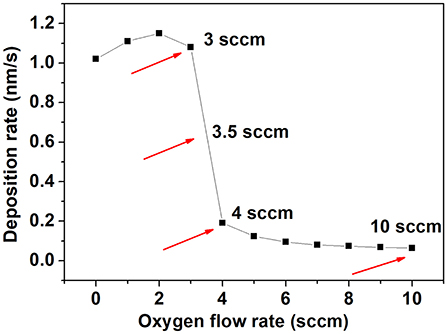
Figure 1. Deposition rate as a function of the oxygen flow rate used to deposit Nb2O5 films.
As can be seen, for rates below 3 sccm the deposition rate is higher (1.1 nm/s). As the oxygen flow rate is increased, the deposition rate decreases. For 3 sccm the rate found is 1.1 nm/s, decreasing abruptly to 0.2 nm/s for 4 sccm. At oxygen flow rates higher than 4 sccm there is only a slight decrease in the deposition rate indicating that from 4 sccm and higher there is an excess of oxygen in the deposition chamber. Films deposited using 3, 3.5, 4, and 10 sccm are denoted 3NbO, 3.5NbO, 4NbO, and 10NbO, respectively.
As previously mentioned, the deposition rate is strongly dependent on the oxygen flow rate. In addition, it can produce different niobium oxide phases such as NbO, NbO2, and Nb2O5, once niobium has three oxidation states: II, IV and V (Foroughi-Abari and Cadien, 2011; Rani et al., 2014; Al-Baradi et al., 2018; Lorenz et al., 2018). With reactive sputtering non-stoichiometric phases can also be produced such as Nb22O54 and Nb12O29 (Rani et al., 2014). From XRD, Figure 2, a phase transition between NbO2 and Nb2O5 is observed in the range of oxygen flow rates used. The most intense diffractions peaks are related to diffractions of FTO (substrate), at 35° one can observe a peak attributed to NbO2 for oxygen flow rates below 3 sccm. As the oxygen flow increases, the Nb2O5 peak located at 28.3° appears and becomes more noticeable in the 10NbO film. Thus, it can be concluded that oxygen flow rates higher than 3 sccm are needed to obtain the Nb2O5 phase. Therefore, NbO2 can be deposited with oxygen flow rates below 3 sccm.
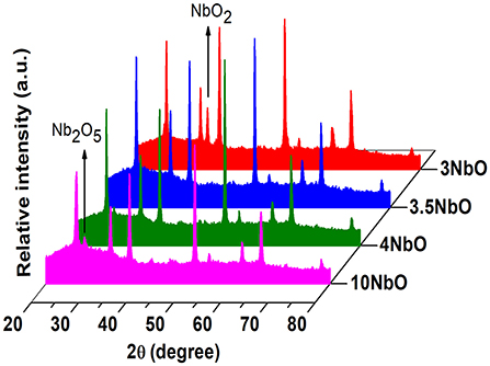
Figure 2. XRD spectra of the niobium oxide films deposited under different oxygens flow rates.
The SEM images of the films are shown in Figures 3a–d. From the images it is possible to observe the similarity between the films, with nanometric spherical particles, apart from the 3NbO that showed sheets shape particles.
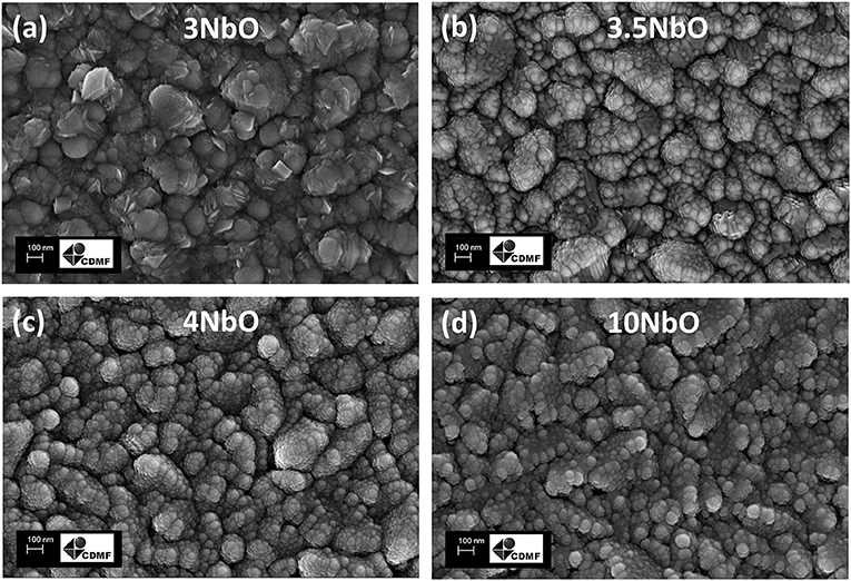
Figure 3. FE-SEM images of the 3NbO (a), 3.5NbO (b), 4NbO (c) and 10 NbO (d).
Figures 4A,B shows the Nb3d and O1s core level XPS spectra of the niobium oxide films. For all samples, two different components can be identified, characteristic of the Nb3d5/2 -Nb3d3/2 doublet, assigned to different bond states of niobium. The peak at ~207eV is related to the Nb5+ oxidation state, and thus to Nb2O5. A careful analysis of the 3NbO spectra (Figure 4A) reveals a broadening of the Nb3d5/2 peak. From the fit (Figure 4C) another component is found at a binding energy of 205eV, which is associated to Nb4+, thus related to NbO2. In fact, as observed in the XRD diffraction, in the 3NbO sample NbO2 is the dominant phase. The presence of the Nb2O5 phase in this sample is most probably due to the oxidation of the surface after exposure to air. Remembering that XPS compared to XRD is much more sensitive to the surface. Furthermore, there is no evidence of the Nb4+ peak for films deposited at oxygen flow rates higher than 3 sccm. From the XPS measurements, as expected, it can be observed the O/Nb ratio increasing as the oxygen flow rate increases, Figure 4D.
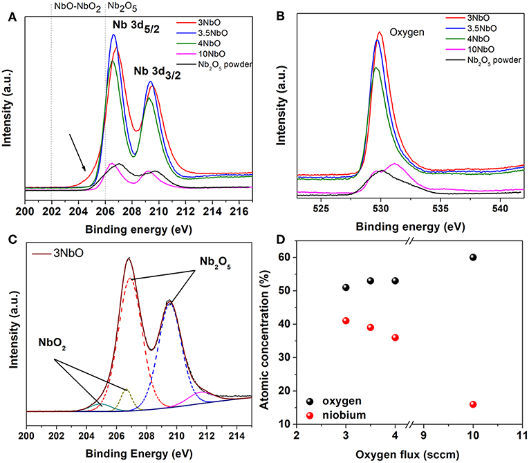
Figure 4. XPS spectra of the niobium oxide films at the Nb 3d edge (A), O 1s edge (B), the fitting curves (dot lines) of the 3NbO film (C) and atomic % of niobium and oxygen for different oxygen flow rates used to deposit the films (D).
Figure 5A shows the transmittance spectra of the films. As expected, the transmittance of 3NbO film is much lower in contrast with the other films. Photographs of the films are shown in Figure 5C, where with the exception of 3NbO the others are transparent in the visible light range. The optical band gap energy of the films (Figure 5B) was calculated using Tauc's plot (Wood and Tauc, 1972). As expected, 3NbO shows a small band gap of ~1.1eV, characteristic of the NbO2 phase. A gap of about 3.77 eV was found for 3.5NbO, 3.72 eV for 4NbO, and 3.69 eV for 10NbO, indicating that in these films Nb2O5 is the dominant phase. Considering the films with larger gaps, there is a slight decrease in the optical band gap with oxygen incorporation. The different gaps may indicate the existence of intermediary energy levels between the valence and conduction bands (Pereira et al., 2018).
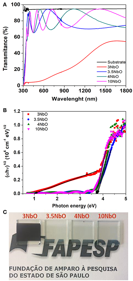
Figure 5. Transmittance spectra (A), Tauc's plot (B) and picture of niobium oxide films (C).
The presence of defects or even the variation of the stoichiometry has a direct influence on the conductivity of the material. It has been reported (Schäfer et al., 1969) that even a small change in the O/Nb ratio resulted in a significant conductivity change. The authors reported a variation from 3 × 10⁻⁶ to 3 × 10³ S/cm by changing the O/Nb ratios from 2.500 to 2.489. Note that these variations in the conductivity were not assigned to metastable phases or phase mixture, instead, to different concentrations of oxygen vacancies in Nb2O5 (Rani et al., 2014).
Different conductivity values of the niobium oxide films were also observed as a function of oxygen flow rate during deposition, Figure 6. As can be seen in Figures 6A,B, the 3NbO has the highest current followed by 3.5NbO while 4NbO has the lowest. From the XRD, 3NbO has NbO2 as the main phase. Electrically, NbO2 is characterized as a semiconductor with high conductivity (Nico et al., 2016). On the other hand, Nb2O5 is typically a semiconductor with low conductivity. From 3.5 to 4 sccm the conductivity decreases as a result of a decrease in oxygen vacancies. As the oxygen flow increases the excess oxygen in the plasma (10 sccm) leads to a slight increase in the conductivity. This effect can be the result of the enhanced electron release from oxygen vacancies and/or oxygen desorption by generation of superoxide species, leading to a decrease in oxygen interstitials. Interstitial oxygen acts as a trap center for free carriers (Terheiden et al., 2014). It is important to notice that this trend is observed in samples deposited at different plasma powers,180 W, and equivalent oxygen flow rate (see Supplementary Materials S1, S2).
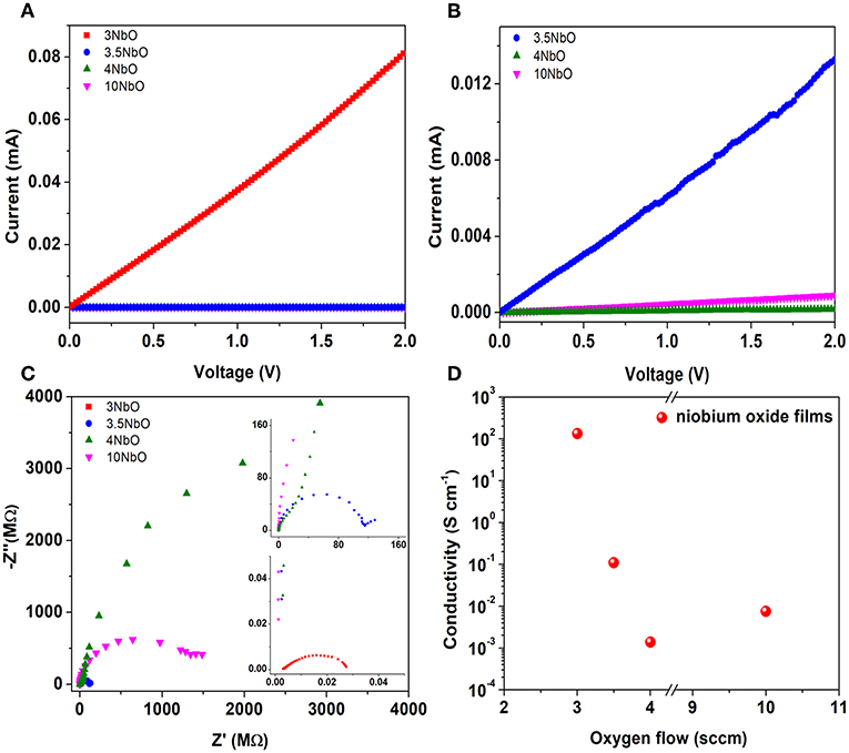
Figure 6. Current-voltage of niobium oxide films (A), zoom of the 3.5NbO-4NbO and 10NbO curves (B), Nyquist plot obtained from impedance spectroscopy (C) and calculated conductivity from current-voltage curves (D).
In Figure 6C, Nyquist plots obtained from impedance spectroscopy are presented. Considering the plot obtained for 3NbO, it is observed a semicircle shape typical from a parallel association of capacitor-resistor. This behavior is more associated with the current flowing through the resistor when the capacitor is fully charged, but in the present case, the resistance is low enough and the current can flow through the resistor before the capacitor be fully charged. This low resistance is associated with NbO2 phase. In the case of 3.5 NbO, when the main phase is Nb2O5, a semicircle shape is also observed followed by a low-frequency tail. This low-frequency tail could be associated with a capacitive charging process at the interface (Huggins, 2002; Wünsche et al., 2015). In 4NbO, the conductive is too small that only capacitive effects are present, no semicircle is observed because the high parallel resistance acts on the radius of the semicircle toward the very-low frequency region. The effect observed for 10 NbO is similar to 3.5 NbO, and it is associated with the slight increase in conductivity, as mentioned before. Furthermore, the conductivity was calculated and the values are shown in Figure 6D. The values were obtained using the relation between resistance (R), conductivity (σ), length (l) and cross-sectional area (A), R = l/σA. The resistance values were obtained through the angular coefficient of the curves obtained in Figures 6A,B.
The niobium oxide films studied were used as ETL in perovskite solar cells. A cross section image of the device is shown inset on Figure 7A. For these solar cells, the 3NbO film was not used since transparency is an essential requirement in ETLs for n-i-p perovskite solar cells.
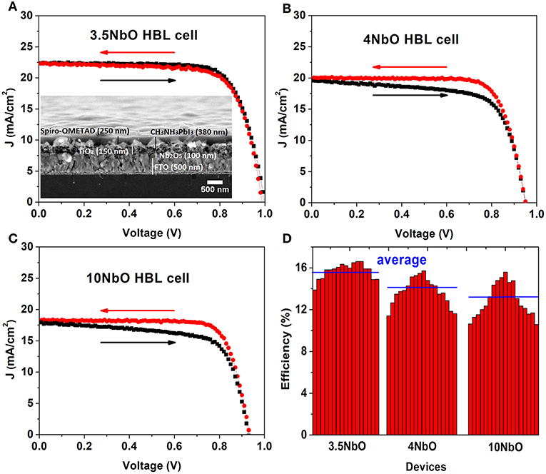
Figure 7. J-V curves of the perovskites solar cells using different niobium oxide ETLs (A–C) and average of the solar cells efficiencies (D).
The J-V curves of the PSCs are presented in Figures 7A–C. Figure 7D shows the solar cell efficiency for different devices. The characteristic parameters summarized in Table 1. Each value presented in this table is the average of 8 different solar cells measurements and the standard deviations are shown in brackets.
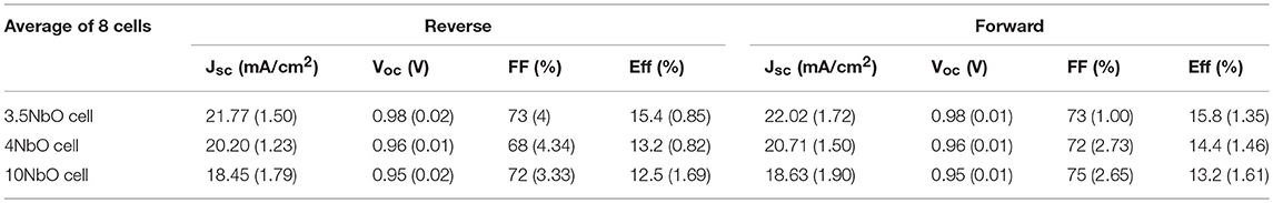
Table 1. Solar cell parameters extracted from J to V measurements of the devices using different niobium oxide hole blocking layers.
From the J-V measurements, there is a clear influence of the ETL on the performance of the cell. The cell made with 3.5NbO HBL has the best performance with the highest current.
The improved performance is attributed to the better conductivity of 3.5NbO ETL. As the resistivity of the niobium oxide films increases there is a decrease in the photocurrent which lowers the efficiency. From the point of maximum power of the J-V curves one can calculate the devices series resistance, this value is minimum for 3.5NbO devices, 290 Ω, and maximum, 410 Ω when 10NbO is used as expected.
As can be seen in Figure 7, the hysteresis of the J-V curve is also dependent on the oxygen flow rate. Hysteresis is the difference in the J-V curve of the forward (from 0 V to Voc) and reverse (from Voc to 0 V) measurements. The J-V hysteresis increases from 3.5 to 10NbO based cells as a response to the decrease in conductivity. In our previous work, we proposed that charge accumulation is responsible for the hysteresis (Fernandes et al., 2016). Here, we attribute the effect to the same mechanism. As the niobium oxide films become less conductive, less photogenerated charges are extracted, accumulating at the interface of HBL-perovskite, thus these charges are responsible for the hysteresis observed in 10 and 4NbO HBL based devices. Note also that in our previous work 50 nm niobium oxide films (equivalent to 10NbO) were necessary to produce good devices. Here, the better charge extraction by 3.5NbO based solar cells allowed devices without hysteresis even when using 100 nm films, which has the advantage of producing films with less pinholes (Fernandes et al., 2016).
In Figure 8 the main solar cell parameters are displayed. It is possible to see that apart from Voc other parameters are directly affected by the niobium oxide ETL. FF slight increases from 0.68 to 0.73, while the Jsc is mostly affected.
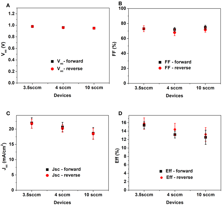
Figure 8. Parameters extracted from J-V curve: Voc, (A), FF (B) Jsc (C) and efficiency (D). The results are an average of 8 cells.
The performance of the solar cell depends on charge transport and injection. PL results, Figure 9, show that the photoluminescence of MAPbI films decreases when the ETLs (mesoporous TiO2/niobium oxide) are put in contact with the perovskite. This result is a clear indication that the emission is suppressed by the charge transfer from MAPbI to ETLs. Electrons photogenerated in perovskite films are first transferred to TiO2 and then to niobium oxide film. As TiO2 is a mesoporous layer, the perovskite infiltrates and remais in contact with niobium oxide, so charges are also transfered directly from perovskite to niobium oxide. Our results show that PL emission is lowest when 3.5NbO/mesoporous TiO2 is used, indicanting that the charge transfer between these films and MAPbI is optimized.
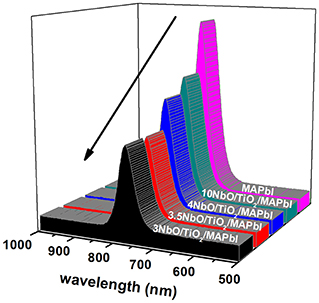
Figure 9. PL photoluminescence of niobium oxide/TiO2/MAPbI perovskite films.
Conclusions
In this work, we have explored the influence of oxygen flow rate used to deposit niobium oxide ETLs and its influence on the performance of the devices. The oxygen flow rate strongly influences niobium oxide electrical conductivity. Considering the films used in the solar cells, 3.5NbO has the highest conductivity which produces solar cells with the highest efficiencies. As a consequence of the better electron extraction, 3.5NbO based devices has low hysteresis.
Author Contributions
SF guided the role study. LGA helped with the data analyses and discussion of niobium oxide conductivity. LJA carried out the deposition rate measurements. JdS conducted the deposition of niobium oxide films. EL and CG helped with the discussion of all the experiments. All the authors contributed to writing and revising the manuscript.
Conflict of Interest Statement
The authors declare that the research was conducted in the absence of any commercial or financial relationships that could be construed as a potential conflict of interest.
Acknowledgments
This work was supported by Fundação de Amparo a Pesquisa do Estado de São Paulo (FAPESP), Centro de Desenvolvimento de Materiais Cerâmicos (CDMF-FAPESP N° 2013/07296-2, 2017/11072-3, 2013/09963-6, and 2017/18916-2). We would like to thank Professor Valmor Roberto Mastelaro (IFSC-USP) and Professor Máximo Siu Li for XPS and PL measurements, respectively.
Supplementary Material
The Supplementary Material for this article can be found online at: https://www.frontiersin.org/articles/10.3389/fchem.2019.00050/full#supplementary-material
References
Al-Baradi, A. M., El-Nahass, M. M., Hassanien, A. M., Atta, A. A., Alqahtani, M. S., and Aldawsari, A. O. (2018). Influence of RF sputtering power on structural and optical properties of Nb2O5thin films. Optik 168, 853–863. doi: 10.1016/j.ijleo.2018.05.020
Asghar, M. I., Zhang, J., Wang, H., and Lund, P. D. (2017). Device stability of perovskite solar cells – A review. Renew. Sust. Energy Rev. 77, 131–146. doi: 10.1016/j.rser.2017.04.003
Burschka, J., Pellet, N., Moon, S.-J., Humphry-Baker, R., Gao, P., Nazeeruddin, M. K., et al. (2013). Sequential deposition as a route to high-performance perovskite-sensitized solar cells. Nature 499, 316–319. doi: 10.1038/nature12340
Fernandes, S. L., Véron, A. C., Neto, N. F. A., Nüesch, F. A., Dias da Silva, J. H., Zaghete, M. A., et al. (2016). Nb2O5hole blocking layer for hysteresis-free perovskite solar cells. Mater. Lett. 181, 103–107. doi: 10.1016/j.matlet.2016.06.018
Foroughi-Abari, A., and Cadien, K. C. (2011). Growth, structure and properties of sputtered niobium oxide thin films. Thin Solid Films 519, 3068–3073. doi: 10.1016/j.tsf.2010.12.036
Green, M. A., Ho-Baillie, A., and Snaith, H. J. (2014). The emergence of perovskite solar cells. Nat. Photonics. 8, 506–514. doi: 10.1038/nphoton.2014.134
Gu, B., Zhu, Y., Lu, H., Tian, W., and Li, L. (2018). Efficient planar perovskite solar cells based on low-cost spin-coated ultrathin Nb2O5films. Solar Energy 166, 187–194. doi: 10.1016/j.solener.2018.03.054
Huggins, R. A. (2002). Simple method to determine electronic and ionic components of the conductivity in mixed conductors a review. Ionics 8, 300–313. doi: 10.1007/BF02376083
Kim, H. S., Im, S. H., and Park, N. G. (2014). Organolead halide perovskite: new horizons in solar cell research. J. Phys. Chem. C 118, 5615–5625. doi: 10.1021/jp409025w
Kogo, A., Numata, Y., Ikegami, M., and Miyasaka, T. (2015). Nb 2 O 5 blocking layer for high open-circuit voltage perovskite solar cells. Chem. Lett. 44, 829–830. doi: 10.1246/cl.150167
Li, D., Liao, P., Shai, X., Huang, W., Liu, S., Li, H., et al. (2016). Recent progress on stability issues of organic–inorganic hybrid lead perovskite-based solar cells. RSC Adv. 6, 89356–89366. doi: 10.1039/C6RA19801E
Lorenz, R., O'Sullivan, M., Fian, A., Sprenger, D., Lang, B., and Mitterer, C. (2018). Effects of bias pulse frequencies on reactively sputter deposited NbOxfilms. Thin Solid Films 660, 335–342. doi: 10.1016/j.tsf.2018.06.040
Nico, C., Monteiro, T., and Graça, M. P. F. (2016). Niobium oxides and niobates physical properties: review and prospects. Progress Mater. Sci. 80, 1–37. doi: 10.1016/j.pmatsci.2016.02.001
Numata, Y., Ishikawa, R., Sanehira, Y., Kogo, A., Shirai, H., and Miyasaka, T. (2018). Nb-doped amorphous titanium oxide compact layer for formamidinium-based high efficiency perovskite solar cells by low-temperature fabrication. J. Mater. Chem. A 6, 9583–9591. doi: 10.1039/C8TA02540A
Park, N. G. (2015). Perovskite solar cells: an emerging photovoltaic technology. Mater. Today18, 65–72. doi: 10.1016/j.mattod.2014.07.007
Pereira, P. F. S., Gouveia, A. F., Assis, M., de Oliveira, R. C., Pinatti, I. M., Penha, M., et al. (2018). ZnWO 4 nanocrystals: synthesis, morphology, photoluminescence and photocatalytic properties. Phys. Chem. Chem. Phys. 20, 1923–1937. doi: 10.1039/C7CP07354B
Rajagopal, A., Yao, K., and Jen, A. K.-Y. (2018). Toward perovskite solar cell commercialization: a perspective and research roadmap based on interfacial engineering. Adv. Mater. 30:e1800455. doi: 10.1002/adma.201800455
Rani, R. A., Zoolfakar, A. S., O'Mullane, A. P., Austin, M. W., and Kalantar-Zadeh, K. (2014). Thin films and nanostructures of niobium pentoxide: fundamental properties, synthesis methods and applications. J. Mater. Chem. A 2, 15683–15703. doi: 10.1039/c4ta02561j
Schäfer, H., Bergner, D., and Gruehn, R. (1969). Beiträge zur chemie der elemente niob und tantal. LXXI. die thermodynamische stabilität der sieben zwischen 2,00 und 2,50 O/Nb existierenden phasen. ZAAC - J. Inorganic General Chem. 365, 31–50.
Wood, D. L., and Tauc, J. (1972). Weak absorption tails in amorphous semiconductors. Phys. Rev. B 5, 3144–3151. doi: 10.1103/PhysRevB.5.3144
Wünsche, J., Deng, Y., Kumar, P., Di Mauro, E., Josberger, E., Sayago, J., et al. (2015). Protonic and electronic transport in hydrated thin films of the pigment eumelanin. Chem. Mater. 27, 436–442. doi: 10.1021/cm502939r
Xiao, G., Shi, C., Lv, K., Ying, C., and Wang, Y. (2018). Nb-doping TiO 2 electron transporting layer for efficient perovskite solar cells. ACS Appl. Energy Mater.1, 2576–2581. doi: 10.1021/acsaem.8b00286
Zhao, X., Park, N.-G., Zhao, X., and Park, N.-G. (2015). Stability issues on perovskite solar cells. Photonics 2, 1139–1151. doi: 10.3390/photonics2041139
Zheng, Y., Kong, J., Huang, D., Shi, W., Mcmillon-Brown, L., Katz, H. E., et al. (2018). Spray coating of the PCBM electron transport layer significantly improves the efficiency of p-i-n planar perovskite solar cells. Nanoscale 10,s 11342–11348. doi: 10.1039/C8NR01763H
Terheiden, B., Hahn, G., Skorka, D., Brinkmann, N., and Gorgulla, A. (2014). “Effect of oxygen during thermal annealing on the electrical and optical properties of sputter deposited Al-Doped ZnO films for heterojunction solar cell application,” in 29th European Photovoltaic Solar Energy Conference and Exhibition. 1076–1080. doi: 10.4229/EUPVSEC20142014-2AV.3.43
Keywords: niobium oxide film, perovskite solar cell, electron transport layer, methyl ammonium lead iodide, reactive sputtering
Citation: Fernandes SL, Albano LGS, Affonço LJ, da Silva JHD, Longo E and Graeff CFdO (2019) Exploring the Properties of Niobium Oxide Films for Electron Transport Layers in Perovskite Solar Cells. Front. Chem. 7:50. doi: 10.3389/fchem.2019.00050
Received: 10 October 2018; Accepted: 18 January 2019;
Published: 06 February 2019.
Edited by:
Sotiris Sotiropoulos, Aristotle University of Thessaloniki, GreeceReviewed by:
Ren Zhang, Intel, United StatesThomas Stergiopoulos, Aristotle University of Thessaloniki, Greece
Copyright © 2019 Fernandes, Albano, Affonço, da Silva, Longo and Graeff. This is an open-access article distributed under the terms of the Creative Commons Attribution License (CC BY). The use, distribution or reproduction in other forums is permitted, provided the original author(s) and the copyright owner(s) are credited and that the original publication in this journal is cited, in accordance with accepted academic practice. No use, distribution or reproduction is permitted which does not comply with these terms.
*Correspondence: Silvia Leticia Fernandes, sy.fernandes@hotmail.com