Band structural and absorption characteristics of antimonene/bismuthene monolayer heterojunction calculated by first-principles
 Yanyan Zhan
 Xuan Fang1,2*
 - 1State Key Laboratory of High Power Semiconductor Lasers, School of Science, Changchun University of Science and Technology, Changchun, China
- 2School of Science and Engineering, The Chinese University of Hong Kong, Shenzhen, China
- 3College of New Materials and New Energies, Shenzhen Technology University, Shenzhen, China
The band gap of lateral heterojunctions (LHSs) can be continuously tuned by changing the widths of their components. In this work, Sb/Bi LHSs based on monolayer Sb and Bi atoms with armchair and zigzag interfaces are constructed, respectively. It exhibits an atom’s number in planner-dependent tunable band gap and near-infrared range absorption characteristics. They are systematically studied by first-principles calculations. The widths are represented by the number (n) of Sb or Bi atom chains. When n increases from 2 to 8, the bandgaps of armchair Sbn/Bin LHSs decrease from 0.89 to 0.67 eV, and the band gaps of zigzag Sbn/Bin LHSs decrease from 0.92 to 0.76 eV. The partial density of states spectra indicate that the occupied states of the valence band are mainly provided by the Bi 6p orbitals. Additionally, the unoccupied states of the conduction band are always provided by the Sb 5p orbitals and Bi 6p orbitals. For Sbn/Bin LHSs, the absorption edge along XX and YY directions move toward the long wavelength direction. These results provide an approach for the applications of two-dimensional materials in near-infrared devices.
Introduction
The influence of quantum confinement effect on the band structure of semiconductor cannot be neglected, especially for tuning of the band gap (Huang et al., 2020; Mu et al., 2018; Agafonov et al., 2010). It is well known that the band gap is caused by quantum confinement effect due to the size. As the size increases, and the band gap decreases (Wu et al., 2005; Wilcoxon et al., 1997). Researchers have used quantum confinement to adjust the band structures of semiconductor materials (Arutyunov et al., 2018; Peng et al., 2018; Chang et al., 2012; Jarolimek et al., 2014). For example, the quantum well is a significant material with a discrete energy level. Its band gaps always decrease as the quantum well thickness increases (Jarolimek et al., 2014). This research indicates that the size of the semiconductor is crucial in adjusting the electronic properties.
Two-dimensional (2D) materials have been intensely studied because of their electronic and optical properties, which can be widely used in optoelectronics, MOSFET, and various devices (Zhang et al., 2021; Das et al., 2015; Shi et al., 2010; Glavin et al., 2020; Zhang et al., 2018; Sturala et al., 2019; Liu et al., 2022; Kumar and Ahluwalia, 2013). It exhibits the numbers of layers dependent on tunable band gaps and variable band structure. For instance, the single-layer MoS2 is a direct band semiconductor, but the bulk MoS2 shows indirect band characteristics (Singh et al., 2012). These phenomena are attributed to the interaction of electrons between layers. Because the layers are connected by Van der Waals forces rather than chemical bonds, the interaction is always weak. The interfaces between layers also increase the electron scattering, which greatly limits the performance of layered materials. But, in the LHSs, the atoms are connected by chemical bonds, which ensures strong electron interaction. A sea of research results show that the electronic properties of 2D materials can be improved with the construction of LHSs (Son et al., 2016; Feng et al., 2021; Guo et al., 2020; Du et al., 2007). However, the size of each component in LHSs has a great influence on the electron interaction due to the limitation of action distance (Zhang et al., 2021; Li et al., 2021; Lee et al., 2017; Bar Yoseph et al., 2014). Therefore, it is meaningful to investigate the band properties of LHSs constructed by various sizes.
In this article, two kinds of single-layer Sb/Bi LHSs composed of monolayer Sb and monolayer Bi with various widths are designed. The widths are represented by n of Sb or Bi atom chains. Initially, the stabilities of Sb/Bi LHSs are proved by formation energies. Then, the band structure, density of states (DOS), and absorption of Sb/Bi LHSs are analyzed in detail by first-principles calculations. It is easy to find that all Sb/Bi LHSs exhibit the feature of direct band structure. Their band gaps are also reduced with an increase in n. For the two types of LHSs, Sbn/Bin LHSs, the occupied states of valence band are mainly provided by the Bi 6p orbitals. Moreover, the unoccupied states of the conduction band are always provided by the Sb 5p orbitals and Bi 6p orbitals. The effect of n on the absorption characteristics of Sb/Bi LHSs is also studied. When n increases, the absorption intensity along the XX direction and the YY direction decreases. Undoubtedly, these Sb/Bi LHSs have potential applications in the field of near-infrared optoelectronic devices.
Computational details
In this article, the first-principles calculations based on the density functional theory (DFT) were performed in the Vienna ab initio simulations package (VASP) (Kresse and Hafner, 1993; Kresse and Furthmüller, 1996). The electron exchange-functional is treated by the Perdew–Burke–Ernzerhof (PBE) functional (Perdew et al., 1993) and described by the generalized gradient approximation (GGA) (Stewart et al., 2005). A cutoff energy of 600 eV was chosen for the plane-wave expansion of wave functions, and the Monkhorst–Pack scheme of k-point sampling was adopted for the integration over the first Brillouin zone. A 2 × 9 × 1k-mesh was used during structural optimization until the energy and Hellman–Feynman force are converged within 10–6 eV and 0.01 eV/Å, respectively (Souadi et al., 2017). In order to minimize the artificial interaction between layers and their periodic images, a vacuum slab of 15 Å along the z-axis was introduced. The electronic band structure, the density of states (DOS), the valence band maximum/the conduction band minimum (VBM/CBM), and the optical absorption spectra of each 2D LHS were calculated by PBE.
Results and discussion
Generally, the properties of LHSs are determined by the nature of the building blocks. Therefore, the LHSs with suitable constituent materials can exhibit unique properties and have a broad application field. In this work, monolayer Sb and monolayer Bi are connected by covalent bonds to form Sbn/Bin LHSs. They have the same hexagonal structures (Bian et al., 2016; Ji et al., 2016; Wu et al., 2017; Tian et al., 2021). For this reason, the sharp hetero-interface and intact hexagonal structures are ensured. Considering the two types of edges, armchair and zigzag, in hexagonal structures, Sbn/Bin LHSs are constructed along the armchair edge and zigzag edge, respectively. The Sb and Bi atom chains alternately appear in the direction perpendicular to the interface. Supplementary Figure S1 schematically illustrates the arrangements of Sbn/Bin LHSs. In Supplementary Figure S1E, their Brillouin zone presents a rectangular structure. The Γ-point is the position of the maximal symmetry point.
High stability is the prerequisite for the construction of LHSs; therefore, the formation energies of all Sbn/Bin LHSs are calculated to first evaluate their stability. As shown in Supplementary Figure S2, the formation energies of all LHSs are negative, which indicates that these LHSs are stable. For armchair structure Sbn/Bin LHSs, the formation energies decreased from −2.498 eV to −2.506 eV when the n is further increased. Moreover, the formation energies of zigzag Sbn/Bin LHSs decreased from −2.498 eV to −2.526 eV. For the two types of Sbn/Bin LHSs, formation energies decrease when n increases from 2 to 8. The calculation results indicated that the constructed LHSs based on Sbn/Bin would be achieved, regardless of the interface atom arrangement.
Based on the stable structures of Sbn/Bin LHSs, we now discuss their electronic properties. The band structures of Sbn/Bin LHSs with armchair and zigzag interfaces are illustrated in Figure 1, Supplementary Figure S3. For armchair structure Sbn/Bin LHSs, they all exhibit direct gap characteristics at the Γ-point. In Figure 1C, their band gaps decrease from 0.89 to 0.67 eV when n is from 2 to 8. Furthermore, the difference between the band gaps of Sb6/Bi6 and that of Sb8/Bi8 is 0.06 eV. It is less than the band gap difference between Sb2/Bi2 and Sb4/Bi4. Considering both effects, the band gaps of Sbn/Bin LHSs decrease when n is further increased. Similarly, the band structures of the zigzag structure Sbn/Bin LHSs are same as those of armchair Sbn/Bin LHSs, except for the value of band gaps. Its band gaps decrease to 0.76 eV as presented in Figure 1F.
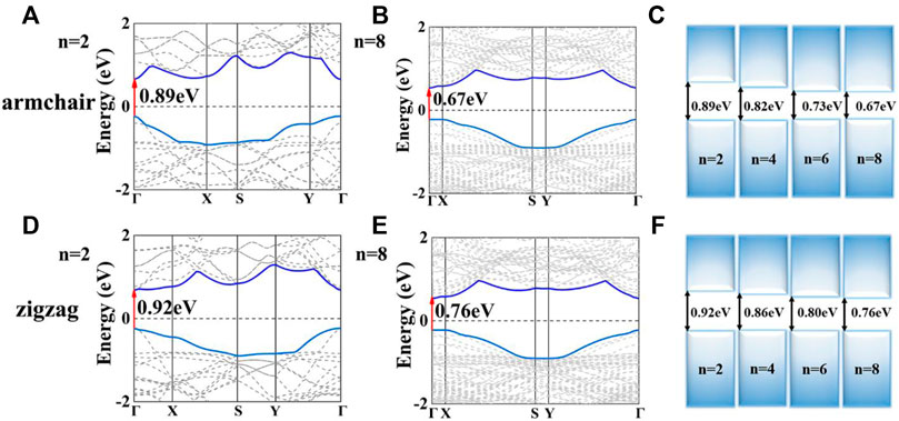
FIGURE 1. (A,B) Band structure of the armchair of Sb2/Bi2 LHSs and Sb8/Bi8 LHSs, respectively; (C) Band gap of the armchair Sb/Bi LHSs under n from 2 to 8; respectively. (D,E) Band structure of the zigzag Sb2/Bi2 LHSs and Sb8/Bi8 LHSs, respectively; (F) Band gap of the zigzag Sb/Bi LHS under n from 2 to 8, respectively.
Supplementary Figure S4 shows the total density of states (TDOS) and partial density of states (PDOS) are studied. For armchair structure Sbn/Bin LHSs, the main occupied state of the valence band of Sb2/Bi2 LHS is provided by the Sb 5p orbital and Bi 6p orbital. Nevertheless, the occupied states of the valence band are mainly provided by the Bi 6p orbitals with the increase in n. In contrast, the unoccupied states of the conduction band are always provided by the Sb 5p orbitals and Bi 6p orbitals. Moreover, the valence band is always close to the Fermi level under n from 2 to 8, which indicates that Sb and Bi atoms form covalent bonds at interfaces. However, there is little shift in the valence band. This further leads to the strong direct interaction of the Sb and Bi atoms through covalent bonds at interfaces. Moreover, the conduction band shifts negatively. This is the direct reason for the reduction in the band gap of Sbn/Bin LHSs. The zigzag structure Sbn/Bin LHSs shows consistent electronic properties.
Next, the band-decomposed partial charge densities for VBM and CBM of two types of LHS are presented in Supplementary Figure S5. For armchair structure Sbn/Bin LHSs, the charges on VBM of Sb2/Bi2 LHS are distributed in an average manner around Sb atoms and Bi atoms in Supplementary Figure S5A1. Supplementary Figure S5A2 presents that the charges on VBM of Sb4/Bi4 LHS are distributed at Bi–Bi bonds and the interface. Moreover, the charges on VBM are all distributed at the Bi–Bi bonds when n = 6 and n = 8. It disappears at the interface between Sb and Bi. Evidently, the charges on VBM gradually transfer to the Bi–Bi bonds. It indicates that the Sbn/Bin LHSs have good electronic properties (Tian et al., 2021). For CBM, the charges of Sb2/Bi2 LHS and Sb4/Bi4 LHS are averagely distributed on Sb atoms and Bi atoms, as illustrated in Supplementary Figures S5B1, B2. However, the charges of Sb6/Bi6 LHS and of Sb8/Bi8 LHS are distributed on Bi atoms and at the interface. In addition, the charges on VBM of zigzag structure Sbn/Bin LHSs show a phenomenon similar with that of armchair structure. The only difference between them is that the charges on VBM show localization on the Bi–Bi bonds for the zigzag structure, as shown in Supplementary Figures S5C2–C4. For CBM of zigzag structure Sbn/Bin LHSs, the charges are averagely distributed on Sb atoms and Bi atoms, regardless of the value of n.
Shown in Figure 2 are the optical absorption spectra of the Sbn/Bin LHSs. For armchair structure Sbn/Bin LHSs, the absorption edges along XX and YY directions are located in the near-infrared range. Furthermore, the absorption edges move toward the long wavelength direction. In this context, the absorption intensity is reduced under n from 2 to 8. The absorption spectrum is found to be consistent with the band gap distribution. Furthermore, the absorption in the XX direction of the Sbn/Bin LHSs is stronger than that in the YY direction. It is reported that the application direction of band gap engineering is related to the carrier transmission direction (Li et al., 2021). When the Sbn/Bin LHSs are designed, the XX direction corresponds to the interface between the Sb and Bi units. Therefore, the transfer of carriers along the XX direction has the greatest possibility. The zigzag structure Sbn/Bin LHSs shows consistent optical absorption properties. The results show that Sbn/Bin LHSs have applications in near-infrared devices.
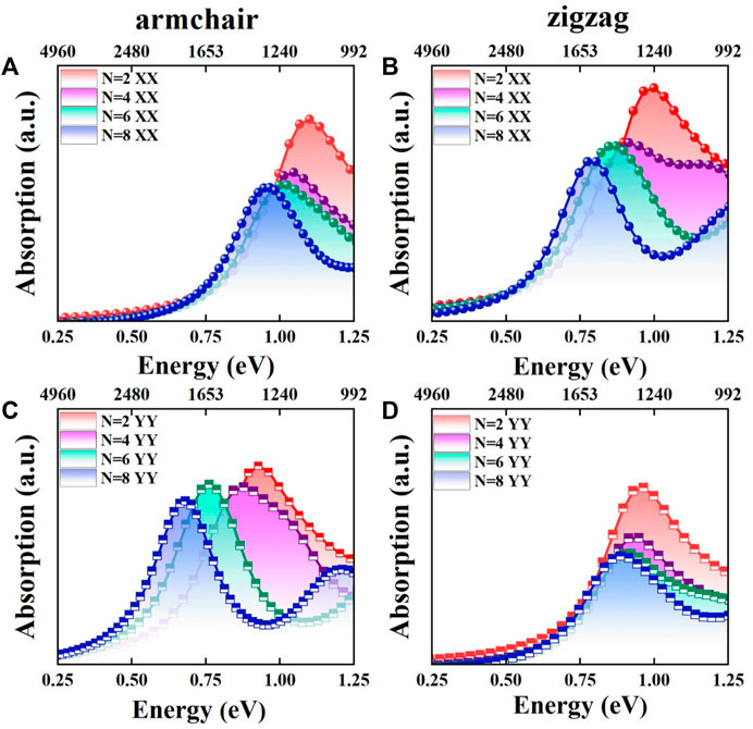
FIGURE 2. (A,C) Absorption spectra of the armchair Sbn/Bin LHSs in XX and YY directions under n from 2 to 8, respectively; (B,D) Absorption spectra of the zigzag Sbn/Bin LHSs in XX and YY directions under n from 2 to 8, respectively.
Conclusion
In conclusion, the band structure, electronic, and optical absorption properties of the Sb/Bi LHSs are determined by the first-principles calculations. Our investigations show that these LHSs are theoretically stable and possible to construct. The structure also becomes more stable with the increasing n. The results show that both armchair and zigzag Sb/Bi LHSs exhibit adjustable direct band gap. Moreover, the band gaps decrease with an increase in n. Then, the PDOS and the VBM/CBM are used to specify the electronic state of Sbn/Bin LHSs. For the two types of LHS, the occupied states of the valence band are provided by the Bi 6p orbitals. Moreover, the unoccupied states of the conduction band are always provided by the Sb 5p orbitals and Bi 6p orbitals. In addition, Sb/Bi LHSs exhibit near-infrared range absorption characteristics. The absorption XX and YY edges move toward the long wavelength direction. Furthermore, it shows that the construction of these LHSs will promote the application of VA group elements in near-infrared optoelectronic devices in the future.
Data availability statement
The raw data supporting the conclusion of this article will be made available by the authors, without undue reservation.
Author contributions
YZ: validation, formal analysis, investigation, data curation, writing—original draft preparation, writing—review and editing, and visualization; XF: conceptualization; DW: conceptualization and validation; DF: supervision; BL: validation and investigation; JL: funding acquisition; and XW: writing—review and editing. All authors have read and agreed to the published version of the manuscript.
Acknowledgments
This work was supported by the National Natural Science Foundation of China (grant numbers 62074018 and 62174015); the Developing Project of Science and Technology of Jilin Province (grant numbers 20200301052RQ and 20210509061RQ); the Natural Science Foundation of Jilin Province (grant numbers 20210101150JC, 20210101473JC, and 20200201266JC); the Guangdong Basic and Applied Basic Research Foundation (grant number 2020A1515010868); the Shenzhen Fundamental Research Fund (grant number JCYJ20180307151538972); the Shenzhen Post doctoral Research Funding (grant number 20211063010010); the University Engineering Research Center of Crystal Growth and Applications of Guangdong Province (grant number 2020GCZX005); the Special Innovative Projects of Guangdong Province (grant number 2020KTSCX125); and the Shenzhen Stable Supporting Program (grant number SZWD2021015).
Conflict of interest
The authors declare that the research was conducted in the absence of any commercial or financial relationships that could be construed as a potential conflict of interest.
Publisher’s note
All claims expressed in this article are solely those of the authors and do not necessarily represent those of their affiliated organizations, or those of the publisher, the editors, and the reviewers. Any product that may be evaluated in this article, or claim that may be made by its manufacturer, is not guaranteed or endorsed by the publisher.
Supplementary material
The Supplementary Material for this article can be found online at: https://www.frontiersin.org/articles/10.3389/fchem.2022.973516/full#supplementary-material
References
Agafonov, O. B., Dais, C., Grützmacher, D., and Haug, R. J. (2010). Quantum confinement effects in Si/Ge heterostructures with spatially ordered arrays of self-assembled quantum dots. Appl. Phys. Lett. 96, 222107. doi:10.1063/1.3442508
Arutyunov, K. Y., Zavialov, V. V., Sedov, E. A., Golokolenov, I. A., Zarudneva, A. A., Shein, K. V., et al. (2018). Nanoarchitecture: Toward quantum‐size tuning of superconductivity. Phys. Status Solidi RRL. 13, 1800317. doi:10.1002/pssr.201800317
Bar-Yoseph, P. Z., Brøns, M., Gelfgat, A., and Oron, A. (2014). Fifth international symposium on bifurcations and instabilities in fluid dynamics (BIFD2013). Fluid Dyn. Res. 46, 041001. doi:10.1088/0169-5983/46/4/041001
Bian, G., Wang, Z. -F., Wang, X. -X., Xu, C. -Z., Xu, S. -Y., Miller, T., et al. (2016). Engineering electronic structure of a TwoDimensional topological insulator Bi(111) bilayer on Sb nanofilms by quantum confinement effect. ACS Nano 10, 3859–3864. doi:10.1021/acsnano.6b00987
Chang, J. -E., Liao, P. -H., Chien, C. -Y., Hsu, J. C., Hung, M. T., Chang, H. -T., et al. (2012). Matrix and quantum confinement effects on optical and thermal properties of Ge quantum dots. J. Phys. D. Appl. Phys. 45, 105303. doi:10.1088/0022-3727/45/10/105303
Das, S., Robinson, J. A., Dubey, M., Terrones, H., and Terrones, M. (2015). Beyond graphene: Progress in novel two-dimensional materials and van der Waals solids. Annu. Rev. Mat. Res. 45, 1–27. doi:10.1146/annurev-matsci-070214-021034
Du, A. J., Smith, S. C., and Lu, G. Q. (2007). First-principle studies of electronic structure and C-doping effect in boron nitride nanoribbon. Chem. Phys. Lett. 447, 181–186. doi:10.1016/j.cplett.2007.09.038
Feng, L. -H., Zhang, X., and Xiang, G. (2021). Electric field tunable bandgap and anisotropic high carrier mobility in SiAs2/GeAs2 lateral heterostructure. Comput. Mat. Sci. 198, 110697. doi:10.1016/j.commatsci.2021.110697
Glavin, N. R., Rao, R., Varshney, V., Bianco, E ., Apte, A., Roy, A., et al. (2020). Emerging applications of elemental 2D materials. Adv. Mat. 32, 1904302. doi:10.1002/adma.201904302
Guo, C., Wei, C., Shen, Y., Cui, X., and Xu, Q. (2020). Fabrication of novel lateral heterostructure of crystallized MoO2/amorphous MoO3-x for photothermal. Convers. Chem. Nano. Mat. 6, 779–782. doi:10.1002/cnma.202000097
Huang, T., Lian, J. -C., Yang, K., Si, Y., Wu, H. -Y., Huang, W. -Q., et al. (2020). From monolayer to lateral heterostructure of functionalized phosphorus carbide: Evolution of electronic properties. Phys. E Low-dimensional Syst. Nanostructures 118, 113962. doi:10.1016/j.physe.2020.113962
Jarolimek, K., Groot, R. A., Wijs, G. A., and Zeman, M. (2014). Quantum confinement and band offsets in amorphous silicon quantum wells. Phys. Rev. B 90, 125430. doi:10.1103/PhysRevB.90.125430
Ji, J. -P., Song, X. -F., Liu, J. -Z., Yan, Z., Huo, C. -X., Zhang, S. -L., et al. (2016). Two-dimensional antimonene single crystals grown by van der Waals epitaxy. Nat. Commun. 7, 13352. doi:10.1038/ncomms13352
Kresse, G., and Furthmüller, J. (1996). Efficient iterative schemes for ab initio total-energy calculations using a plane-wave basis set. Phys. Rev. B 54, 11169–11186. doi:10.1103/PhysRevB.54.11169
Kresse, G., and Hafner, J. (1993). Ab. initio molecular dynamics for liquid metals. Phys. Rev. B 47, 558–561. doi:10.1103/physrevb.47.558
Kumar, A., and Ahluwalia, P. K. (2013). Semiconductor to metal transition in bilayer transition metals dichalcogenides MX2 (M =Mo, W; X = S, Se, Te). Model. Simul. Mat. Sci. Eng. 21, 065015. doi:10.1088/0965-0393/21/6/065015
Lee, J., Huang, J. S., Sumpter, B. G., and Yoon, M. (2017). Strain-engineered optoelectronic properties of 2D transition metal dichalcogenide lateral heterostructures. 2D Mat. 4, 021016. doi:10.1088/2053-1583/aa5542
Li, W. -J., Fang, X., Wang, D. -K., Tian, F., Wang, H., Fang, D., et al. (2021). Band and optical properties of arsenene and antimonene lateral heterostructure by first-principles calculations. Phys. E Low-dimensional Syst. Nanostructures 134, 114933. doi:10.1016/j.physe.2021.114933
Liu, J. -S., Tian, F., Wang, D. -K., Fang, D., Fang, X., Zhao, H. -B., et al. (2022). First principles studies on infrared band structure and absorption of As/Sb lateral heterostructures. J. Appl. Phys. 131, 023101. doi:10.1063/5.0076063
Mu, C., Wei, W., Li, J. -J., Huang, B., and Dai, Y. (2018). Electronic properties of two-dimensional in-plane heterostructures of WS2/WSe2/MoS2. Mat. Res. Express 5, 046307. doi:10.1088/2053-1591/aabddf
Peng, G., Yu, X., He, Y. L., Li, G. Y., Liu, Y. X., Zhang, X., et al. (2018). Quantum confinement effect in β-SiC nanowires. Front. Phys. 13, 137802. doi:10.1007/s11467-018-0768-0
Perdew, J. P., Chevary, J. A., Vosko, S. H., Jackson, K. A., Pederson, M. R., Singh, D. J., et al. (1993). Erratum: Atoms, molecules, solids, and surfaces: Applications of the generalized gradient approximation for exchange and correlation. Phys. Rev. B 48, 4978. doi:10.1103/physrevb.48.4978.2
Shi, Y., Hamsen, C., Jia, X., Kim, K. K., Reina, A., Hofmann, M., et al. (2010). Synthesis of few-layer hexagonal boron nitride thin film by chemical vapor deposition. Nano Lett. 10, 4134–4139. doi:10.1021/nl1023707
Singh, N., Jabbour, G., and Schwingenschlögl, U. (2012). Antimonene: A monolayer material for ultraviolet optic nanodevices. Eur. Phys. J. B 85, 392. doi:10.1140/epjb/e2012-30449-7
Son, Y., Li, M. -Y., Cheng, C. -C., Wei, K. -H., Liu, P., Wang, Q. -H., et al. (2016). Observation of switchable photoresponse of a monolayer WSe2-MoS2 lateral heterostructure via photocurrent spectral atomic force microscopic imaging. Nano Lett. 16, 3571–3577. doi:10.1021/acs.nanolett.6b00699
Souadi, Z., Bouhemadou, A., and Khenata, R. (2017). Structural, elastic and lattice dynamical properties of the alkali metal tellurides: First-principles study Y. Al-Douri. Phys. B 521, 204. doi:10.1016/j.physb.2017.07.004
Stewart, J. I., Matthew, D. S., Chris, J. P., Phil, J. H., Matt, I. J., Refson, V. K., et al. (2005). First principles methods using CASTEP. Res. Gate. 21, 567–570. doi:10.1524/zkri.220.5.567.65075
Sturala, J., Sofer, Z., and Pumera, M. (2019). Coordination chemistry of 2D and layered gray arsenic: Photochemical functionalization with chromium hexacarbonyl. NPG Asia Mat. 11, 42. doi:10.1038/s41427-019-0142-x
Tian, F., Wang, D. -K., Tan, F. -X., Fang, X., Li, W.-J., Wang, H.-Z., et al. (2021). Strain-dependent band structures and electronic properties in Sb/Bi lateral heterostructures calculated by first principles. Phys. Status Solidi RRL. 15, 2100148. doi:10.1002/pssr.202100148
Wilcoxon, J. P., Newcomer, P. P., and Samara, G. A. (1997). Synthesis and optical properties of MoS2 and isomorphous nanoclusters in the quantum confinement regime. J. Appl. Phys. 81, 7934–7944. doi:10.1063/1.365367
Wu, X. -L., Fan, J. -Y., Qiu, T., Yang, X., Siu, G. -G., Chu, P. -K., et al. (2005). Experimental evidence for the quantum confinement effect in 3C-SiC nanocrystallites. Phys. Rev. Lett. 94, 026102. doi:10.1103/PhysRevLett.94.026102
Wu, X., Shao, Y., Liu, H., Feng, Z. -L., Wang, Y. -L., Su, J. -T., et al. (2017). Epitaxial Growth and air-stability of monolayer antimonene on PdTe2. Adv. Mat. 29, 1605407. doi:10.1002/adma.201605407
Zhang, B. -W., Fang, D., Fang, X., Zhao, H. -B., Wang, D. -K., Li, J. -H., et al. (2021a). InAs/InAsSb type-II superlattice with near room-temperature long-wave emission through interface engineering. Rare Met. 41, 982–991. doi:10.1007/s12598-021-01833-x
Zhang, F., Huang, Y., Zheng, K., Cui, H., Guo, H., Yu, J., et al. (2021b). Monolayer h-BN/C3B lateral heterostructures with promising electronic and optical properties: A firstprinciples study. Chem. Phys. 541, 111042. doi:10.1016/j.chemphys.2020.111042
Keywords: antimonene (Sb), bismuthene (Bi), lateral heterojunction, band structure, optical absorption, first-principles calculations
Citation: Zhan Y, Fang X, Wang D, Fang D, Li B, Li J and Wang X (2022) Band structural and absorption characteristics of antimonene/bismuthene monolayer heterojunction calculated by first-principles. Front. Chem. 10:973516. doi: 10.3389/fchem.2022.973516
Received: 21 June 2022; Accepted: 04 July 2022;
Published: 05 August 2022.
Edited by:
Haichang Zhang, Qingdao University of Science and Technology, ChinaReviewed by:
Liang Guo, Jilin Jianzhu University, ChinaZhikun Xu, Guangdong University of Petrochemical Technology, China
Copyright © 2022 Zhan, Fang, Wang, Fang, Li, Li and Wang. This is an open-access article distributed under the terms of the Creative Commons Attribution License (CC BY). The use, distribution or reproduction in other forums is permitted, provided the original author(s) and the copyright owner(s) are credited and that the original publication in this journal is cited, in accordance with accepted academic practice. No use, distribution or reproduction is permitted which does not comply with these terms.
*Correspondence: Xuan Fang, fangx@cust.edu.cn; Dengkui Wang, wangdk@cust.edu.cn