The prediction of two-dimensional PbN: opened bandgap in heterostructure with CdO
 Zhang Cheng1
  Ruxin Zheng
 Weihua Mu
- 1Department of Automotive and Mechanical Engineering, Anhui Communications Vocational & Technical College, Hefei, China
- 2Faculty of Mechanical and Electrical Engineering, Hainan Vocational University of Science and Technology, Haikou, China
- 3School of Mechanical Engineering, Southeast University, Nanjing, China
- 4Wenzhou Institute, University of Chinese Academy of Sciences, Wenzhou, China
The development of two-dimensional (2D) materials has received wide attention as a generation of optoelectronics, thermoelectric, and other applications. In this study, a novel 2D material, PbN, is proposed as an elemental method using the prototype of a recent reported nitride (J. Phys. Chem. C 2023, 127, 43, 21,006–21014). Based on first-principle calculations, the PbN monolayer is investigated as stable at 900 K, and the isotropic mechanical behavior is addressed by the Young’s modulus and Poisson’s ratio at 67.4 N m–1 and 0.15, respectively. The PbN monolayer also presents excellent catalytic performance with Gibbs free energy of 0.41 eV. Zero bandgap is found for the PbN monolayer, and it can be opened at about 0.128 eV by forming a heterostructure with CdO. Furthermore, the PbN/CdO is constructed by Van der Waals interaction, while the apparent potential drop and charge transfer are investigated at the interface. The PbN/CdO heterostructure also possesses excellent light absorption properties. The results provide theoretical guidance for the design of layered functional materials.
1 Introduction
After the discovery of graphene (Geim and Novoselov, 2009), two-dimensional (2D) materials have received much investigation due to its remarkable electronic (Ghosh et al., 2015; Ambrosi et al., 2017), optical (Mogulkoc et al., 2016), mechanical (Sun et al., 2017), and catalytic (Lathe et al., 2023) properties and a wide range of applications. For example, black phosphorus possesses a puckered structure, which can be prepared by electrochemical method under a field effect transistor. The thickness of black phosphorus can reach several nanometers, and the highest carrier mobility can be as high as 104 cm2·v−1·s–1 (Xiao et al., 2015). At room temperature, black phosphorus more than 7.5 nm thick presents excellent transistor performance, and the leakage current modulation is of 105 order (Li et al., 2014; Jia et al., 2015; Carvalho et al., 2016; Clark et al., 2018). As the allotrope of black phosphorus, blue phosphorus is hexagonal in plane and has a bandgap of 2.77 eV (Ren et al., 2019a). The hopping parameters of the TB Hamiltonian of blue phosphorus are extracted by density functional theory (DFT), and it has been found that the energy band of blue phosphorus can be tuned by the applied electric field (Ding and Wang, 2015; Li et al., 2015; Liu et al., 2015; Zhu et al., 2016; Xiong et al., 2017; Yang et al., 2017; Safari et al., 2019). The arsenene also shows a honeycomb structure and has an indirect bandgap in both bending and folding states (Kamal and Ezawa, 2015), which can be further tuned by applying strain. It is worth noting that 1% external strain can transform the puckered arsenene into a direct semiconductor (Kamal and Ezawa, 2015; Zhang et al., 2015; Wang et al., 2017; Xu et al., 2017; Wang et al., 2018; Zhang et al., 2018). All this demonstrates that 2D materials have favorable prospects in optoelectronics and thermoelectric nanodevices.
In order to further expand the application of these 2D materials and discover more unusual mechanical, optical, and electronic properties, many strategies have been explored to predict and develop new 2D materials (Miao and Sun, 2022). Wu et al. (2016) have predicted a family of titanium silicide (Ti2Si, TiSi2, and TiSi4) monolayers through the calculation of DFT, in which Ti2Si is a ferromagnetic metal, and the magnetic moment is obtained as 1.37 μB/cell. TiSi2 has been proven to be an ideal catalyst with excellent hydrogen evolution reaction performances. Importantly, TiSi4 can be used as a powerful 2D phonon-mediated superconductor; its transition temperature is calculated as 5.8 K, and the transition temperature in particular can be increased to 11.7 K by applying a certain strain. Luo et al. (2011) used the global optimization method to predict 2D boron carbon. The calculation results demonstrate that BC compounds exhibit metal properties. In addition, BC3 shows semiconductor properties, and the most stable BC structure possesses high thermal stability even above 2000 K. Based on evolutionary search and first principles, Sun and Schwingenschlögl (2020) predicted an anisotropic Janus structure material B2P6, which is a semiconductor with an indirect bandgap of 2.09 eV. Interestingly, the Janus structure can induce an inherent electric field, which significantly inhibits the recombination of optical source carriers. It is also proven that B2P6 can be used as a promising photocatalyst for water splitting, with an excellent solar-to-hydrogen efficiency of 28.2%. Lu et al. (2018) predicted a 2D material CaP3, which has a direct bandgap of 1.15 eV and ultrahigh electron mobility of about 2.0 × 104 cm2·v−1·s–1. Jing et al. (2017) proposed a GeP3 semiconductor with an indirect bandgap of 0.55 eV. It is notable that GeP3 can transform the indirect bandgap into the direct bandgap under the condition of biaxial strain. GeP3 also has remarkable light absorption ability and can be widely used in the field of optoelectronics.
In this study, we propose a new 2D material named PbN by the elemental method with the prototype of the recent reported XN monolayers (Ren et al., 2023a). Using first-principle calculations, the stability and structural parameters are addressed. Then, the mechanical, electronic, and catalytic performances are investigated. The Van der Waals based on the PbN and CdO monolayers is constructed with an opened tiny bandgap, which also possesses excellent optical properties. The results show that the PbN/CdO van der Waals heterostructure is promising as an optical nano-sensor.
2 Computational methods
All simulations in this work were carried out by the first-principles method, which is employed by density functional theory (DFT) (Grest et al., 1981; Capelle, 2006). The calculation instrument is the Vienna Ab initio simulation package (VASP) (Van de Walle and Martin, 1989), which is embedded with the projector-augmented wave method (Kresse and Furthmüller, 1996a; Kresse and Joubert, 1999; Grimme et al., 2010). The Perdew–Burke–Ernzerhof functional was considered by utilizing the generalized gradient approximation means (Kresse and Furthmüller, 1996b; Perdew et al., 1996; Grimme, 2006). The phonon spectra of the system under study were explored by the density functional perturbation theory (DFPT), which is obtained by PHONOPY code (Togo et al., 2008; Togo and Tanaka, 2015). In calculations of the band structure of the studied heterostructure, the Heyd–Scuseria–Ernzerhof hybrid functional (Heyd et al., 2005) was explored to calculate a more precise bandgap, and the DFT-D3 method was considered for the heterostructure to address the weak dispersion forces proposed by Grimme et al. (2010). To simulate the Gibbs free energy of the studied system, the DFT-D3 method of Grimme was explored to consider the Van der Waals interactions in all calculations, and the dipole-corrected functional was also adopted (Van de Walle and Martin, 1989). The energy cut-off was selected as 550 eV, and the Monkhorst–Pack k-point grid is 17 × 17 × 1 in the first Brillouin zone. The vacuum height was adopted by 25 Å, which can effectively prevent forces between adjacent layers. The convergence for force was used by 0.01 eV Å−1, and the energy of the calculated system was controlled in 0.01 meV.
3 Results and discussion
The predicted atomic structure of the PbN monolayer is shown in Figure 1A, constructed by the elemental method (Ren et al., 2022a). This crystal structure of the PbN monolayer is honeycombed with a space group of P3m1, inspired by the SiN monolayer prototype (Ren et al., 2023a). It is worth noting that there is also a possibility that the PbN monolayer possesses other phase structures, but we just focused on the crystal structures of the predicted NSi monolayer prototype. The cohesive energy E) of the PbN monolayer is calculated by E = [EN2 + EPb bulk − EPbN/2], where EPbN, EN2, and EPb bulk are the total energy of the PbN system, N2, and Pb bulk, respectively. After the optimization of the PbN monolayer, the obtained cohesive energy of the PbN monolayer is 6.41 eV/atom, which is comparable to early synthesized 2D materials like MoS2 (about 5.02 eV/atom) (Sun and Schwingenschlögl, 2021) and SiN (about 5.56 eV/atom) (Ren et al., 2023a). Importantly, the cohesive energies of the monolayered PbN show an energetic stability, which presents a feasibility in experimental preparation. The lattice constant obtained for the monolayered PbN is calculated as 3.653 Å, which is larger than that of the MoS2 monolayer (3.180 Å) (Ren et al., 2019b). The simulated scanning tunneling microscopy (STM) appearance of the monolayered PbN with 3 × 3 supercell is expressed by Figure 1B, which is beneficial for identifying the structure of the PbN monolayer in future experiments. Furthermore, the phonon dispersion of the PbN monolayer is calculated to verify dynamic stabilities (Togo et al., 2008; Togo and Tanaka, 2015), suggested as Figure 1C. It can be seen that no imaginary frequency is obtained in the phonon dispersion, explaining a dynamic stability of the PbN monolayer. It is worth noting that the highest frequency of the PbN monolayer is comparable with that of SnN (Ren et al., 2023a).
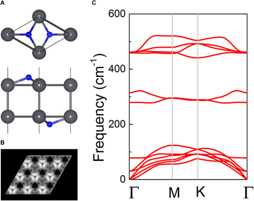
Figure 1. (A) Atomic structure of the PbN monolayer; gray and blue balls are Pb and N atoms, respectively. (B) Simulated STM images of the PbN crystal structures under the bias of −2 V. (C) Calculated phonon spectrum of the PbN monolayer.
Investigating the stability of the PbN monolayer requires not only consideration of the cohesive and phonon spectrum but also the thermal property that requires further study. Thus, AIMD calculations are conducted for further exploration. The PbN system is constructed by a 5 × 5 × 1 supercell with 100 atoms in the simulations to prevent the lattice translational constraints (Li et al., 2023). The heat bath scheme is selected by the Nosé–Hoover method (Nosé, 1984). After completing the calculations, the relaxed structure of the monolayered PbN is still undamaged at 300 K, 600 K, and 900 K (Figures 2A–C, respectively) for 10 ps. The obtained temperature and total energy are monitored as stable in the AIMD calculation, suggesting a robust thermal stability of the predicted PbN monolayer.
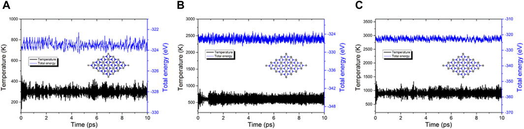
Figure 2. Temperature and energy in AIMD simulations of the PbN monolayer at (A) 300 K, (B) 600 K, and (C) 900 K; the insets are AIMD snapshots of the PbN, the gray and blue balls are Pb and N atoms, respectively.
We next investigated the mechanical performance of the PbN monolayer by calculating Young’s modulus E) and Poisson’s ratio v), defined as:
where θ is the angle beginning the x-direction. Young’s modulus and Poisson’s ratio of the PbN monolayer are expressed by Figures 3A,B, respectively. One can see that Young’s modulus and Poisson’s ratio of the PbN monolayer do not present directional dependence, suggesting isotropic mechanical property (Ren et al., 2023a). The calculated Young’s modulus and Poisson’s ratio of the PbN monolayer are 67.4 N m–1 and 0.15, respectively. Such a small Young’s modulus of the PbN monolayer forced the nanocomponents, while it is still higher than that of ZnO (47.8 N m–1) (Peng et al., 2013). The obtained Poisson’s ratio of the PbN monolayer is also smaller than that of MX2Y4 monolayers (0.264–0.327) (Ren et al., 2023b) and larger than that of the CN monolayer (about 0.12) (Ren et al., 2023a). The strain effect of the PbN monolayer is also calculated along the x and y directions. Even if the PbN monolayer presents an apparently isotropic Young’s modulus and Poisson’s ratio, the fracture property is different along the x and y directions. Shown as Figure 3C, the PbN monolayer exhibits significant fracture stress about 7 N m–1 at 14% along the x direction, while it only has yield limit in the y direction of about 6 N m–1 at 13%. It is worth noting that in the small strain range, the slopes in both the x and y directions are the same, which also confirms the equality of the Young’s modulus of the PbN monolayer (Sun et al., 2020).
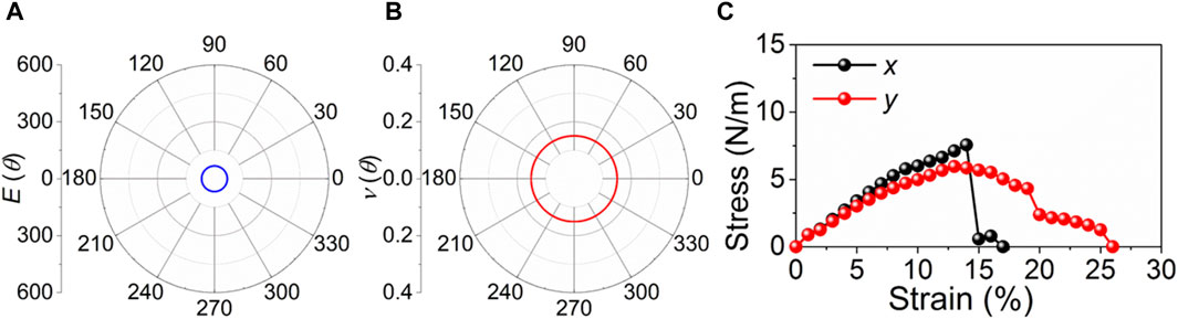
Figure 3. Calculated (A) Young’s moduli, (B) Poisson’s ratios, and (C) strain–stress relationships along the x and y directions of the PbN monolayer.
The band structure of the PbN monolayer is then calculated by HSE06 calculations (Figure 4A). On can see that the Fermi level passes through the band energy with a zero-bandgap characteristic. The hydrogen evolution reaction performance of the PbN monolayer is further explored considering the active adsorption point marked by the cyan balls in Figure 4B. Obviously, four different representative active adsorption points are addressed by the highly symmetrical structure. The Gibbs free energy changes (ΔGH*) of the PbN monolayer are decided at standard conditions using
where the energy of the H adsorbed PbN monolayer is ΔE. The difference of the zero-point energy is expressed by ΔEzpe. The difference in the entropy by the hydrogen evolution reaction is ΔS. In this study, T is considered 298.15 K in the simulations. The active site is demonstrated by “*”. Thus, the hydrogen evolution reaction process is finished by two reactions:
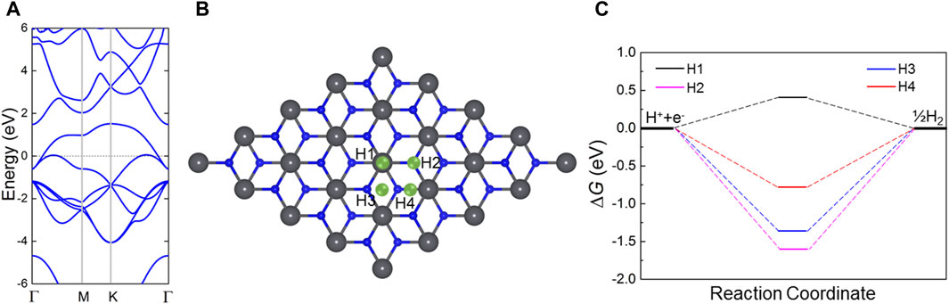
Figure 4. (A) Calculated band structure of PbN monolayer; Fermi level is 0. (B) Representative adsorption sites in hydrogen evolution reaction of the PbN monolayer. (C) Calculated Gibbs free energies of the PbN monolayer in the hydrogen evolution reaction.
The most stable HER adsorption configuration is decided via binding energy (Eb), which is calculated by Eb = Esystem – Epure – EH, where Esystem, Epure, and EH represent the energy of the adsorbed PbN system, pure PbN monolayer, and single H atom, respectively. The lower binding energy implies a more stable structure; thus, the most stable HER adsorption site is obtained by the system with lowest binding energy in the H1 site. After the calculations, the Gibbs free energy of the PbN monolayer with these active sites is obtained as Figure 4C. The PbN monolayer possesses excellent catalytic performance, with Gibbs free energy of 0.41 eV at the H1 active site, which is even more favorable than that of the biphenylene network (about 2.93 eV) (Ren et al., 2022b) and graphene (about 1.41 eV) (Luo et al., 2021).
Considering that the lattice constant of the monolayered PbN as 3.653 Å is comparable with that of the CdO monolayer (3.684 Å) (Ren et al., 2021), the Van der Waals (vdWs) heterostructure formed by the PbN and CdO monolayers is feasible. Thus, the lattice mismatch is only about 0.8% in the PbN/CdO heterostructure, while six different representative stacking structures of the PbN/CdO heterostructure should be considered by high symmetry (Figure 5)—NC-1, NC-2, NC-3, NC-4, NC-5, and NC-6. For NC-1, the PbN/CdO heterostructure is constructed by the O and Cd atoms on the top of the lower and upper N atoms, respectively. Then, the NC-2 PbN/CdO heterostructure is formed by the O and Cd atoms on top of the Nb and upper N atoms, respectively. In NC-3 PbN/CdO heterostructure, the O and Cd atoms are located on top of the Nb and lower N atoms, respectively. The O and Cd atoms are on top of the upper N and the lower N, and the NC-4 PbN/CdO heterostructure is obtained. For the NC-5 PbN/CdO heterostructure, the O and Cd atoms are fixed on top of the upper N and Nb atoms, respectively. Furthermore, the NC-6 PbN/CdO heterostructure can be constructed by locating the O and Cd atoms on top of the lower N and Nb atoms, respectively.
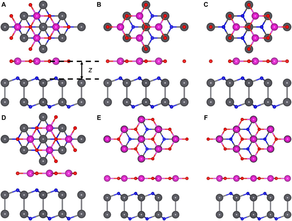
Figure 5. Stacked PbN/CdO heterostructure with representative structures (A) NC-1, (B) NC-2, (C) NC-3, (D) NC-4, (E) NC-5, (F) NC-6. Gray, blue, red, and purple balls are Pb, N, O, and Cd atoms, respectively.
To determine the most stable PbN/CdO heterostructure with these six different configurations, the binding energy E) of the PbN/CdO heterostructure is considered by E = EPbN/CdO − EPbN − ECdO, where EPbN/CdO, EPbN, and ECdO are the energy of the PbN/CdO system, pure PbN, and CdO monolayers, respectively. The obtained binding energy of the PbN/CdO heterostructure is −30.11 meV/Å2 for NC-2 configuration, which is lower than that of graphene (about −18 meV/Å2) (Chen et al., 2013). Thus, the PbN/CdO heterostructure is constructed by vdWs interactions. In addition, the distance of the interface and bond length of these different stacking configurations of the optimized PbN/CdO heterostructure and pure PbN, CdO monolayers are calculated in Table 1. The obtained interfacial high of the NC-2 PbN/CdO heterostructure is 2.414 Å, which is smaller than that of the CdO/HfS2 vdW heterostrutcure (about 2.86 Å) (Zhang et al., 2022a). The following calculations are based on this structure.
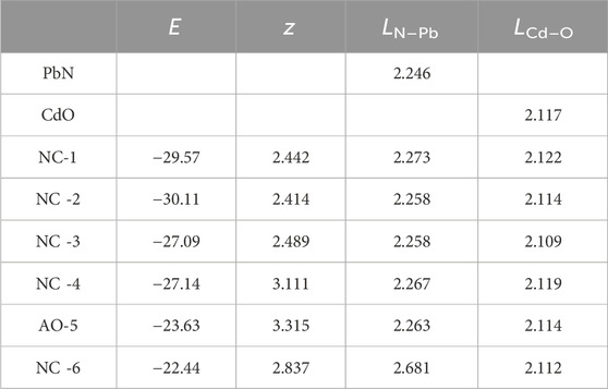
Table 1. Obtained binding energy (E, meV/Å2), distance of interface (z, Å), and bond length (L, Å) of the PbN/CdO heterostructure with different stacking styles and pure PbN, CdO.
The band energy of the PbN/CdO vdWs heterostructure is calculated in Figure 6A; interestingly, a very small bandgap (about 0.128 eV) is found. Furthermore, the projected band structure of the PbN/CdO vdWs heterostructure is calculated in Figure 6B using the HSE06 functional. It can be seen that the slight bandgap results from the PbN layer, meaning that the bandgap of the PbN monolayer can be opened by forming a vdWs heterostructure with the CdO monolayer. Thus, the PbN/CdO vdWs heterostructure is a potential candidate for use as a sensor in nano-devices. In Figure 6C, the potential difference across the interface of the PbN/CdO vdWs heterostructure is obtained as 5.323 eV, which is larger than that of other reported heterostructures, such as MoTe2/PtS2 (4.41–4.67 eV) (Ren et al., 2022c), MoTe2/PtS2 (4.67 eV) (Zhang et al., 2022b), and CdO/HfS2 (5.23 eV) (Zhang et al., 2022a). Furthermore, the charge density difference (Δρ) of the PbN/CdO vdWs heterostructure was also investigated, demonstrated by Δρ = ρPbN/CdO − ρPbN − ρCdO, where ρPbN/CdO, ρPbN and ρCdO being the total charge of the PbN/CdO system, and the pure PbN and CdO monolayers, respectively. The results show that CdO obtains considerable electrons (about 13.619) by Bader-charge analysis (Sanville et al., 2007). This also explains the larger potential drop across the interface of the PbN/CdO vdWs heterostructure in Figure 6C. Such desirable potential drop is also of great assistance for carrier migration between the interface of the PbN/CdO vdWs heterostructure. The tiny bandgap in the PbN/CdO vdWs heterostructure compared to the wide bandgap in the CdO monolayer (about 2.073 eV) can also enhance the light absorption properties, expressed as
where ω is used as the angular frequency, α is the absorption coefficient, and the speed of light is demonstrated by c.
where
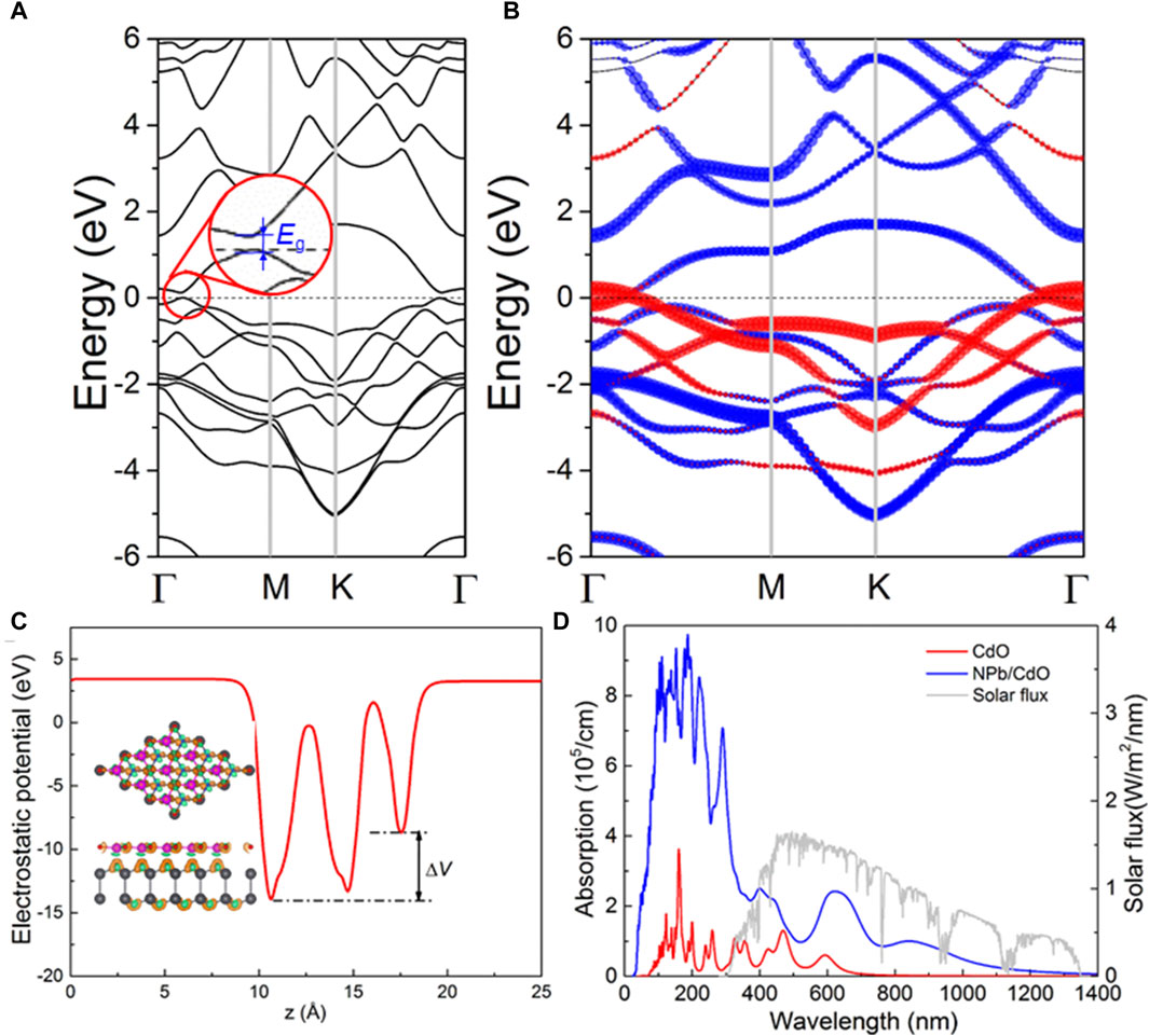
Figure 6. Calculated (A) band structure and (B) projected band structure of PbN/CdO vdW heterostructure; red and blue marks are contributed PbN and CdO monolayers, respectively. (C) Potential drop of PbN/CdO vdW heterostructure; inset is the isosurface lever for charge difference in the PbN/CdO vdW heterostructure, the orange and blue ones represent the gain and loss of electrons, respectively. (D) HSE06 obtained optical absorption coefficient of the PbN/CdO vdW heterostructure.
4 Conclusion
A novel 2D nitride, PbN, is predicted in this investigation. Structure and stability is systematically studied with the PbN monolayer presenting dynamic and thermal stability at 900 K. The Young’s modulus and Poisson’s ratio of the PbN monolayer are calculated as 67.4 N m–1 and 0.15, respectively. The excellent catalytic performance of the PbN monolayer is also obtained with the Gibbs free energy of 0.41 eV. The PbN monolayer is formed as a heterostructure with a CdO monolayer, which is constructed by vdW forces. The PbN/CdO can open a tiny bandgap for the PbN (about 0.128 eV), and the predominant light absorption performances is also addressed. The results show that the PbN monolayer has potential as an optical sensor.
Data availability statement
The original contributions presented in the study are included in the article/Supplementary Material; further inquiries can be directed to the corresponding author.
Author contributions
ZC: writing–original draft, writing–review and editing, and funding acquisition. YW: formal analysis, investigation, supervision, and writing–review and editing. RZ: data curation, methodology, and writing–review and editing. WM: funding acquisition, supervision, validation, and writing–original draft.
Funding
The author(s) declare financial support was received for the research, authorship, and/or publication of this article. The authors are grateful for funding of the Universities and Key Project of Natural Science Research of Anhui Provincial Department of Education (Project numbers: 2023AH052966) and High-level Talent Project of Hainan Provincial Natural Science Foundation (Project number: 521RC610). WM is grateful for the startup grant from Wenzhou Institute, University of Chinese Academy of Sciences (Project number. WIUCASQD2021024).
Conflict of interest
The authors declare that the research was conducted in the absence of any commercial or financial relationships that could be construed as a potential conflict of interest.
Publisher’s note
All claims expressed in this article are solely those of the authors and do not necessarily represent those of their affiliated organizations, or those of the publisher, the editors, and the reviewers. Any product that may be evaluated in this article, or claim that may be made by its manufacturer, is not guaranteed or endorsed by the publisher.
References
Ambrosi, A., Sofer, Z., and Pumera, M. (2017). Electrochemical exfoliation of layered black phosphorus into phosphorene. Angew. Chem. Int. Ed. 56, 10443–10445. doi:10.1002/anie.201705071
Capelle, K. (2006). A bird's-eye view of density-functional theory. Braz. J. Phys. 36, 1318–1343. doi:10.1590/s0103-97332006000700035
Carvalho, A., Wang, M., Zhu, X., Rodin, A. S., Su, H., and Neto, A. H. C. (2016). Phosphorene: from theory to applications. Nat. Rev. Mat. 1, 16061–16116. doi:10.1038/natrevmats.2016.61
Chen, X., Tian, F., Persson, C., Duan, W., and Chen, N. X. (2013). Interlayer interactions in graphites. Sci. Rep. 3, 3046. doi:10.1038/srep03046
Clark, N., Nguyen, L., Hamer, M. J., Schedin, F., Lewis, E. A., Prestat, E., et al. (2018). Scalable patterning of encapsulated black phosphorus. Nano Lett. 18, 5373–5381. doi:10.1021/acs.nanolett.8b00946
Ding, Y., and Wang, Y. (2015). Structural, electronic, and magnetic properties of adatom adsorptions on black and blue phosphorene: a first-principles study. J. Phys. Chem. C 119, 10610–10622. doi:10.1021/jp5114152
Geim, A., and Novoselov, K. (2009). The rise of graphene. Nat. Mater 6, 183–191. doi:10.1038/nmat1849
Ghosh, B., Nahas, S., Bhowmick, S., and Agarwal, A. (2015). Electric field induced gap modification in ultrathin blue phosphorus. Phys. Rev. B 91, 115433. doi:10.1103/physrevb.91.115433
Grest, G., Nagel, S., Rahman, A., and Witten, T. (1981). Density of states and the velocity autocorrelation function derived from quench studies. J. Chem. Phys. 74, 3532–3534. doi:10.1063/1.441508
Grimme, S. (2006). Semiempirical GGA-type density functional constructed with a long-range dispersion correction. J. Comput. Chem. 27, 1787–1799. doi:10.1002/jcc.20495
Grimme, S., Antony, J., Ehrlich, S., and Krieg, H. (2010). A consistent and accurate ab initio parametrization of density functional dispersion correction (DFT-D) for the 94 elements H-Pu. J. Chem. Phys. 132, 154104. doi:10.1063/1.3382344
Heyd, J., Peralta, J. E., Scuseria, G. E., and Martin, R. L. (2005). Energy band gaps and lattice parameters evaluated with the Heyd-Scuseria-Ernzerhof screened hybrid functional. J. Chem. Phys. 123, 174101. doi:10.1063/1.2085170
Jia, J., Jang, S. K., Lai, S., Xu, J., Choi, Y. J., Park, J.-H., et al. (2015). Plasma-treated thickness-controlled two-dimensional black phosphorus and its electronic transport properties. ACS Nano 9, 8729–8736. doi:10.1021/acsnano.5b04265
Jing, Y., Ma, Y., Li, Y., and Heine, T. (2017). GeP3: a small indirect band gap 2D crystal with high carrier mobility and strong interlayer quantum confinement. Nano Lett. 17, 1833–1838. doi:10.1021/acs.nanolett.6b05143
Kamal, C., and Ezawa, M. (2015). Arsenene: two-dimensional buckled and puckered honeycomb arsenic systems. Phys. Rev. B 91, 085423. doi:10.1103/physrevb.91.085423
Kresse, G., and Furthmüller, J. (1996a). Efficiency of ab-initio total energy calculations for metals and semiconductors using a plane-wave basis set. Comp. Mat. Sci. 6, 15–50. doi:10.1016/0927-0256(96)00008-0
Kresse, G., and Furthmüller, J. (1996b). Efficient iterative schemes for ab initio total-energy calculations using a plane-wave basis set. Phys. Rev. B 54, 11169–11186. doi:10.1103/physrevb.54.11169
Kresse, G., and Joubert, D. (1999). From ultrasoft pseudopotentials to the projector augmented-wave method. Phys. Rev. B 59, 1758–1775. doi:10.1103/physrevb.59.1758
Lathe, A., Palanisamy, K., Prakash, M., and Palve, A. M. (2023). Photocatalytic activities of cadmium (II) acetophenone thiosemicarbazone complex: experimental and density functional theory based study. Inorg. Chem. Commun. 155, 111064. doi:10.1016/j.inoche.2023.111064
Li, J., Pan, H., Sun, H., Zheng, R., and Ren, K. (2023). First-principle study of two-dimensional SiP2 for photocatalytic water splitting with ultrahigh carrier mobility. Crystals 13, 981. doi:10.3390/cryst13060981
Li, L., Yu, Y., Ye, G. J., Ge, Q., Ou, X., Wu, H., et al. (2014). Black phosphorus field-effect transistors. Nat. Nanotechnol. 9, 372–377. doi:10.1038/nnano.2014.35
Li, Q.-F., Duan, C.-G., Wan, X. G., and Kuo, J.-L. (2015). Theoretical prediction of anode materials in Li-ion batteries on layered black and blue phosphorus. J. Phys. Chem. C 119, 8662–8670. doi:10.1021/jp512411g
Liu, L. Z., Wu, X. L., Liu, X. X., and Chu, P. K. (2015). Strain-induced band structure and mobility modulation in graphitic blue phosphorus. Appl. Surf. Sci. 356, 626–630. doi:10.1016/j.apsusc.2015.08.125
Lou, J., Ren, K., Huang, Z., Huo, W., Zhu, Z., and Yu, J. (2021). Electronic and optical properties of two-dimensional heterostructures based on Janus XSSe (X = Mo, W) and Mg(OH)2: a first principles investigation. Rsc. Adv. 11, 29576–29584. doi:10.1039/d1ra05521f
Lu, N., Zhuo, Z., Guo, H., Wu, P., Fa, W., Wu, X., et al. (2018). CaP3: a new two-dimensional functional material with desirable band gap and ultrahigh carrier mobility. J. Phys. Chem. Lett. 9, 1728–1733. doi:10.1021/acs.jpclett.8b00595
Luo, X., Yang, J., Liu, H., Wu, X., Wang, Y., Ma, Y., et al. (2011). Predicting two-dimensional boron-carbon compounds by the global optimization method. J. Am. Chem. Soc. 133, 16285–16290. doi:10.1021/ja2072753
Luo, Y., Ren, C., Xu, Y., Yu, J., Wang, S., and Sun, M. (2021). A first principles investigation on the structural, mechanical, electronic, and catalytic properties of biphenylene. Sci. Rep. 11, 19008. doi:10.1038/s41598-021-98261-9
Miao, N., and Sun, Z. (2022). Computational design of two-dimensional magnetic materials. Wiley Interdiscip. Rev. Comput. Mol. Sci. 12, e1545. doi:10.1002/wcms.1545
Mogulkoc, Y., Modarresi, M., Mogulkoc, A., and Ciftci, Y. O. (2016). Electronic and optical properties of bilayer blue phosphorus. Comp. Mat. Sci. 124, 23–29. doi:10.1016/j.commatsci.2016.07.015
Nosé, S. (1984). A unified formulation of the constant temperature molecular dynamics methods. J. Chem. Phys. 81, 511–519. doi:10.1063/1.447334
Peng, Q., Liang, C., Ji, W., and De, S. (2013). A first principles investigation of the mechanical properties of g-ZnO: the graphene-like hexagonal zinc oxide monolayer. Comp. Mat. Sci. 68, 320–324. doi:10.1016/j.commatsci.2012.10.019
Perdew, J. P., Burke, K., and Ernzerhof, M. (1996). Generalized gradient approximation made simple. Phys. Rev. Lett. 77, 3865–3868. doi:10.1103/physrevlett.77.3865
Ren, K., Ma, X., Liu, X., Xu, Y., Huo, W., Li, W., et al. (2022a). Prediction of 2D IV–VI semiconductors: auxetic materials with direct bandgap and strong optical absorption. Nanoscale 14, 8463–8473. doi:10.1039/d2nr00818a
Ren, K., Ren, C., Luo, Y., Xu, Y., Yu, J., Tang, W., et al. (2019a). Using van der Waals heterostructures based on two-dimensional blue phosphorus and XC (X= Ge, Si) for water-splitting photocatalysis: a first-principles study. Phys. Chem. Chem. Phys. 21, 9949–9956. doi:10.1039/c8cp07680d
Ren, K., Shu, H., Huang, L., Wang, K., Luo, Y., Huo, W., et al. (2023a). Predicted XN (X = C, Si, Ge, and Sn) monolayers with ultrahigh carrier mobility: potential photocatalysts for water splitting. J. Phys. Chem. C 127, 21006–21014. doi:10.1021/acs.jpcc.3c06284
Ren, K., Shu, H., Huo, W., Cui, Z., and Xu, Y. (2022b). Tuning electronic, magnetic and catalytic behaviors of biphenylene network by atomic doping. Nanotechnology 33, 345701. doi:10.1088/1361-6528/ac6f64
Ren, K., Shu, H., Wang, K., and Qin, H. (2023b). Two-dimensional MX2Y4 systems: ultrahigh carrier transport and excellent hydrogen evolution reaction performances. Phys. Chem. Chem. Phys. 25, 4519–4527. doi:10.1039/d2cp04224j
Ren, K., Sun, M., Luo, Y., Wang, S., Yu, J., and Tang, W. (2019b). First-principle study of electronic and optical properties of two-dimensional materials-based heterostructures based on transition metal dichalcogenides and boron phosphide. Appl. Surf. Sci. 476, 70–75. doi:10.1016/j.apsusc.2019.01.005
Ren, K., Yu, J., and Tang, W. (2020). Two-dimensional ZnO/BSe van der waals heterostructure used as a promising photocatalyst for water splitting: a DFT study. J. Alloys Compd. 812, 152049. doi:10.1016/j.jallcom.2019.152049
Ren, K., Zheng, R., Yu, J., Sun, Q., and Li, J. (2021). Band bending mechanism in CdO/arsenene heterostructure: a potential direct Z-scheme photocatalyst. Front. Chem. 9, 788813. doi:10.3389/fchem.2021.788813
Ren, K., Zhu, Z., Wang, K., Huo, W., and Cui, Z. (2022c). Stacking-mediated type-I/Type-II transition in two-dimensional MoTe2/PtS2 heterostructure: a first-principles simulation. Crystals 12, 425. doi:10.3390/cryst12030425
Safari, F., Moradinasab, M., Fathipour, M., and Kosina, H. (2019). Adsorption of the NH3, NO, NO2, CO2, and CO gas molecules on blue phosphorene: a first-principles study. Appl. Surf. Sci. 464, 153–161. doi:10.1016/j.apsusc.2018.09.048
Sanville, E., Kenny, S. D., Smith, R., and Henkelman, G. (2007). Improved grid-based algorithm for Bader charge allocation. J. Comput. Chem. 28, 899–908. doi:10.1002/jcc.20575
Sun, M., Chou, J. P., Yu, J., and Tang, W. (2017). Electronic properties of blue phosphorene/graphene and blue phosphorene/graphene-like gallium nitride heterostructures. Phys. Chem. Chem. Phys. 19, 17324–17330. doi:10.1039/c7cp01852e
Sun, M., and Schwingenschlögl, U. (2020). B2P6: a two-dimensional anisotropic Janus material with potential in photocatalytic water splitting and metal-ion batteries. Chem. Mat. 32, 4795–4800. doi:10.1021/acs.chemmater.0c01536
Sun, M., and Schwingenschlögl, U. (2021). Structure prototype outperforming MXenes in stability and performance in metal-ion batteries: a high throughput study. Adv. Energy Mater. 11, 2003633. doi:10.1002/aenm.202003633
Sun, M., Yan, Y., and Schwingenschlogl, U. (2020). Beryllene: a promising anode material for Na-and K-ion batteries with ultrafast charge/discharge and high specific capacity. J. Phys. Chem. Lett. 11, 9051–9056. doi:10.1021/acs.jpclett.0c02426
Togo, A., Oba, F., and Tanaka, I. (2008). First-principles calculations of the ferroelastic transition between rutile-type and CaCl2-type SiO2 at high pressures. Phys. Rev. B 78, 134106. doi:10.1103/physrevb.78.134106
Togo, A., and Tanaka, I. (2015). First principles phonon calculations in materials science. Scr. Mater. 108, 1–5. doi:10.1016/j.scriptamat.2015.07.021
Van de Walle, C. G., and Martin, R. M. (1989). ‘‘Absolute’’deformation potentials: formulation and ab initio calculations for semiconductors. Phys. Rev. Lett. 62, 2028–2031. doi:10.1103/physrevlett.62.2028
Wang, X., He, J., Zhou, B., Zhang, Y., Wu, J., Hu, R., et al. (2018). Bandgap-tunable preparation of smooth and large two-dimensional antimonene. Angew. Chem. 57, 8668–8673. doi:10.1002/anie.201804886
Wang, Y., Huang, P., Ye, M., Quhe, R., Pan, Y., Zhang, H., et al. (2017). Many-body effect, carrier mobility, and device performance of hexagonal arsenene and antimonene. Chem. Mat. 29, 2191–2201. doi:10.1021/acs.chemmater.6b04909
Wu, Q., Zhang, J. J., Hao, P., Ji, Z., Dong, S., Ling, C., et al. (2016). Versatile titanium silicide monolayers with prominent ferromagnetic, catalytic, and superconducting properties: theoretical prediction. J. Phys. Chem. Lett. 7, 3723–3729. doi:10.1021/acs.jpclett.6b01731
Xiao, J., Long, M., Zhang, X., Ouyang, J., Xu, H., and Gao, Y. (2015). Theoretical predictions on the electronic structure and charge carrier mobility in 2D phosphorus sheets. Sci. Rep. 5, 9961. doi:10.1038/srep09961
Xiong, P.-Y., Chen, S.-Z., Zhou, W.-X., and Chen, K.-Q. (2017). Semiconductor-metal transition induced by giant Stark effect in blue phosphorene nanoribbons. Phys. A 381, 2016–2020. doi:10.1016/j.physleta.2017.04.032
Xu, Y., Peng, B., Zhang, H., Shao, H., Zhang, R., and Zhu, H. (2017). First-principle calculations of optical properties of monolayer arsenene and antimonene allotropes. Ann. Phys-Berlin 529, 1600152. doi:10.1002/andp.201600152
Yang, G., Xu, Z., Liu, Z., Jin, S., Zhang, H., and Ding, Z. (2017). Strain- and fluorination-induced quantum spin Hall insulators in blue phosphorene: a first-principles study. J. Phys. Chem. C 121, 12945–12952. doi:10.1021/acs.jpcc.7b03808
Zhang, G., Yu, M.-B., Tung, C.-H., and Lo, G.-Q. (2008). Quantum size effects on dielectric constants and optical absorption of ultrathin silicon films. IEEE Electron Device Lett. 29, 1302–1305. doi:10.1109/led.2008.2005651
Zhang, L., Ren, K., Li, J., Cui, Z., and Cheng, H. (2022b). The first-principles study of external strain tuning the electronic and optical properties of the 2D MoTe2/PtS2 van der Waals heterostructure. Front. Chem. 10, 934048. doi:10.3389/fchem.2022.934048
Zhang, Q., Ren, K., Zheng, R., Huang, Z., An, Z., and Cui, Z. (2022a). First-principles calculations of two-dimensional CdO/HfS2 van der Waals heterostructure: direct Z-scheme photocatalytic water splitting. Front. Chem. 10, 879402. doi:10.3389/fchem.2022.879402
Zhang, S., Guo, S., Chen, Z., Wang, Y., Gao, H., Gomez-Herrero, J., et al. (2018). Recent progress in 2D group-VA semiconductors: from theory to experiment. Chem. Soc. Rev. 47, 982–1021. doi:10.1039/c7cs00125h
Zhang, S., Yan, Z., Li, Y., Chen, Z., and Zeng, H. (2015). Atomically thin arsenene and antimonene: semimetal-semiconductor and indirect-direct band-gap transitions. Angew. Chem. 54, 3112–3115. doi:10.1002/anie.201411246
Keywords: two-dimensional materials, PBN, mechanical properties, heterostructure, applications
Citation: Cheng Z, Wang Y, Zheng R and Mu W (2024) The prediction of two-dimensional PbN: opened bandgap in heterostructure with CdO. Front. Chem. 12:1382850. doi: 10.3389/fchem.2024.1382850
Received: 06 February 2024; Accepted: 27 March 2024;
Published: 18 April 2024.
Edited by:
Shu Wang, Harbin University of Science and Technology, ChinaReviewed by:
Anil Mahadeo Palve, Mahatma Phule Arts Science and Commerce College, IndiaMenglong Zhang, South China Normal University, China
Copyright © 2024 Cheng, Wang, Zheng and Mu. This is an open-access article distributed under the terms of the Creative Commons Attribution License (CC BY). The use, distribution or reproduction in other forums is permitted, provided the original author(s) and the copyright owner(s) are credited and that the original publication in this journal is cited, in accordance with accepted academic practice. No use, distribution or reproduction is permitted which does not comply with these terms.
*Correspondence: Weihua Mu, muwh@ucas.ac.cn