Charge transport comparison of FA, MA and Cs lead halide perovskite single crystals for radiation detection
 Stephanie H. Bennett1
  Joydip Ghosh1
  Eric Gros-Daillon2
  Ferdinand Lédée2
  Javier Mayén Guillén3 Jean-Marie Verilhac3
  Julien Zaccaro4
  Duck Young Chung5 Vladislav Klepov6 Mercouri G. Kanatzidis5,6
  Paul J. Sellin1*
- 1Department of Physics, University of Surrey, Guildford, United Kingdom
- 2University Grenoble Alpes, CEA, Leti, Grenoble, France
- 3University Grenoble Alpes, CEA, Liten, Grenoble, France
- 4Grenoble Alpes University, CNRS, Grenoble INP, Institut Néel, Grenoble, France
- 5Materials Science Division, Argonne National Laboratory, Evanston, IL, United States
- 6Department of Chemistry, Northwestern University, Evanston, IL, United States
We report a systematic comparison of the charge transport and radiation detection properties of inorganic and organic metal bromide single crystal perovskites. We studied the performance of Bridgman-grown CsPbBr3 single crystals, together with solution-grown FAPbBr3 and MAPbBr3 single crystals. Laser time of flight is used to measure the drift mobilities for all samples, and we report a maxium mobility value of 121 ± 10 cm V−1 s−1 for CsPbBr3. Alpha particle measurements were used to assess the mobility-lifetime products, with values recorded in the range of 2 × 10⁻⁴ cm2 V−1 to 1 × 10⁻³ cm2 V−1. Low temperature measurements showed an increase in bulk resistivity at temperatures down to 260 K, but no significant change to the drift mobilities. The overall performance of the Cs, FA and MA samples is compared and their potential for use in gamma spectroscopy measurements is discussed.
1 Introduction
The progress of metal halide perovskites (structure ABX3) has accelerated over the last few years, due to their promising characteristics and potential applications in medical imaging, nuclear security and industrial inspection. These materials show the required high resistivity and high mobility-lifetime products that are required for use as X-ray and gamma ray detectors (Yakunin et al., 2016). For a comparison of the typical properties of traditional compound semiconductors used for X-ray and gamma ray detection, the reader is referred to the review article in reference (Sellin and Vaitkus, 2006). The wide range of applications of these materials has also been helped by their ability to operate at room temperature making them portable and relatively low cost. Most research so far has focused on lead halide perovskites, which have a high Z-number making them good candidates for X-ray and gamma ray detection.
Inorganic based perovskites, with Cs on the A-site, have good environmental stability (thermal, moisture and light) as they do not contain volatile organic cations (Wang et al., 2020). Generally the lead halide perovskites all exhibit structural phase transitions, between orthorhombic, tetragonal and cubic structures, as shown in Table 1. Cs-based lead halides undergo these phase transitions between approximately 360 K–400 K which can potentially cause stress and cracking in the crystals during growth, particularly when high temperature Bridgman methods are used. In contrast the organic based perovskites, with molecules such as formamidinium (FA) or methylammonium (MA) on the A-site, benefit from having phase change transitions below room temperature. Of the two organic perovskites, FA-based has previously been reported to show better environmental stability (Zhang et al., 2018), whilst both FA and MA based lead halides appear to show broadly similar charge transport properties (Musiienko et al., 2019).
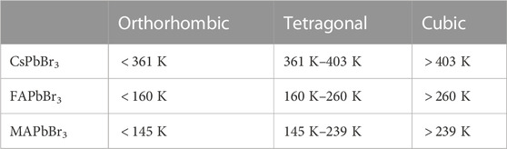
TABLE 1. Phase change temperatures of Cs, FA and MA based single crystal samples. Data acquired from: CsPbBr3 (Whitcher et al., 2019), FAPbBr3 (Schueller et al., 2018), MAPbBr3 (Keshavarz et al., 2019).
In this work we systematically compare the charge transport properties, and suitability as radiation detectors, of these three perovskite lead halide single crystals. We study the influence of the cation in lead bromide perovskite structures, specifically comparing FAPbBr3 (denoted as FA in this paper), MAPbBr2.55Cl0.45 (denoted as MA) and CsPbBr3 (denoted as Cs) single crystals. The MA sample was blended with a small amount of chloride as this was observed to improve the stability of the samples. A typical solution-grown FAPbBr3 single crystal is shown in Figure 1, demonstrating good optical transparency and the absence of internal stress in the crystal.
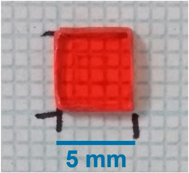
FIGURE 1. Typical FAPbBr3 single crystal showing good transparency.
We compare the charge transport properties of all three perovskite types and report measurements of resistivity, drift mobility, and mobility-lifetime product. The influence of these charge transport parameters is discussed in terms of their operation as radiation detectors, including their X-ray photocurrent sensitivity and their spectroscopic response for alpha particles and gamma rays.
2 Methodology
The perovskite lead halide single crystals (sizes up to 6 mm × 6 mm) used in this work were FAPbBr3, MAPbBr2.55Cl0.45 and CsPbBr3. Five samples of FAPbBr3 were grown at the University of Surrey using the Inverse Temperature Crystallisation method (ITC), 4 samples of MAPbBr2.55Cl0.45 (MA) were grown at CEA/CNRS using the ITC method (Mayen Guillén et al., 2023) and 4 samples of CsPbBr3 (Cs) were grown at Northwestern University using the Bridgman growth method.
The FA and Cs samples were prepared with sputtered Au-Au electrodes and the MA samples with Cr-Cr electrodes, with a planar device structure. The devices were fixed to support boards with colloidal graphite paint for electrical measurements. Current-voltage (I-V) measurements were conducted with a Keithley SourceMeter (model 2,400 series) with the samples mounted in a cryostat for low temperature measurements. The I-V scans were conducted in a pulsed method from 0 V bias to applied bias and back to 0 V bias with a dwell time of 15 s between each bias reading, which was used to minimise ion migration in the crystals.
X-ray sensitivity measurements were conducted by irradiating the devices with 100 ms X-ray pulses at 4 Hz, corresponding to 24 µGyair dose per pulse with RQA5 spectrum (70 kV accelerating voltage, 23.5 mm Al filtration), shown in Figure 2. The mean energy of the X-ray beam was 52.6 keV (Rosado et al., 2007). The incident X-ray dose in air was calibrated using a PTW Unidos dosimeter, with a calibration uncertainty of ±3%. The experimental setting follows the characteristic medical radiography setups described in IEC 62220 International Standard. The integration of the photocurrent over the pulse duration yields the measured charge Q. In order to reduce experimental errors, each photocurrent measurement was repeated and the measured charge Q averaged over 10 pulses, with an uncertainty on the averaged charge measurement of ±10%.
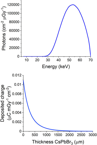
FIGURE 2. (upper) Modelled filtered RQA5 X-ray energy spectrum at 70 kV, using 23.5 mm aluminium filtration, (lower) depth profile of the deposited charge due to absorbed X-rays in CsPbBr3 where 2/3 of the incident X-rays are absorbed within 350 μm of the surface. The spectrum was calculated using the SpekCalc software (Poludniowski and Evans, 2007a; Poludniowski and Evans, 2007b).
Laser time of flight (ToF) measurements were conducted with a 1 Hz pulsed blue 405 nm 30 mW semiconductor laser (PTI Inc), with a 100 ns pulse duration. The bias was pulsed from 0 V bias, to the applied bias for 10 ms, then to 0 V bias, and was synchronised with the laser rate. The resulting current pulses were amplified using a Femto RF current amplifier (DHPCA-100, BW = 14 MHz, V/A = 105). For the Cs samples, ToF was carried out using a137Cs gamma source to replace the laser, and with the pulses fed into a charge integrating preamplifier (Kromek eV-550, see the Supplementary Material for more details of this technique). All ToF pulses were captured using a high speed waveform digitiser (CAEN 5730) and analysed using offline event-by-event software. For low temperature measurements the samples were mounted in a liquid-nitrogen continuous flow cryostat. ToF was also conducted in a constant bias mode to observe the effects of changing field distribution. With the bias voltage applied to the opposite electrode as the laser irradiation, positive/negative applied bias corresponded to pulses due to electron/hole transport, respectively.
Alpha particle spectroscopy was carried out using a241Am source mounted approximately 1 cm from the device surface. Alpha spectra were acquired with the signal passed through a charge sensitive preamplifier (Kromek eV-550) and into the digital pulse processor (Amptek PX-4). Alpha pulse shapes were acquired using the CAEN 5730 waveform digitiser. The samples were mounted in a cryostat to allow for low temperature measurements. Gamma spectroscopy was carried out with the same instrumentation as for alpha spectroscopy, except for use of a low noise CoolFET A250CF preamplifier. Three gamma sources were used, 241Am, 57Co and 137Cs.
3 Results
3.1 Dark current
I-V measurements showed linear behaviour for all three sample types, with resistivities of 2.4 × 10⁹ Ωcm (MA), 5.7 × 10⁹ Ωcm (FA) and 1.5 × 10¹⁰ Ωcm (Cs), shown in Figure 3. In general Cs showed the lowest dark current followed by FA and MA. In all three samples current hysteresis was minimal due to the pulsed biasing technique described in the Methodology section.
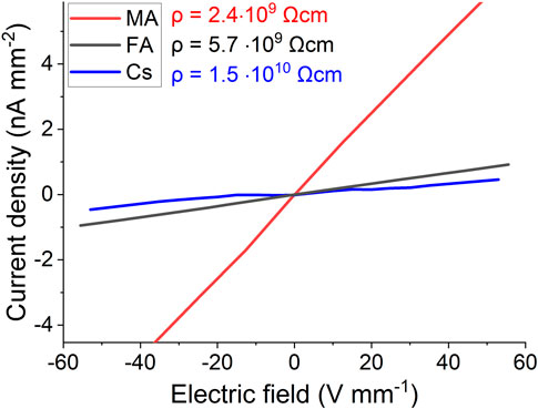
FIGURE 3. Current density against electric field of the three sample types MA, FA and Cs. At 10 V mm−1, dark current densities are 1.5 nA mm−2 (MA), 0.5 nA mm−2 (FA) and 0.1 nA mm−2 (Cs).
Low temperature I-V was conducted to study the influence of traps in the temperature region 295 K–220 K. Figure 4A) shows the reduction in dark current in the FA sample at lower temperatures leading to an increase in the resistivities, shown in Figure 4B). The FA resistivity strongly increases at lower temperatures whereas the MA and Cs remains approximately constant. It is unlikely that the cause of this increase in resistivity of the FA sample is related to its phase change (cubic-tetragonal) at 260 K, since the MA sample did not experience a similar resistivity change and has a similar phase change (cubic-tetragonal) at 239 K. It is possible that this temperature dependant change in resistivity seen in FA is due to ‘freezing’ of traps that are contributing to the charge transport at room temperature.
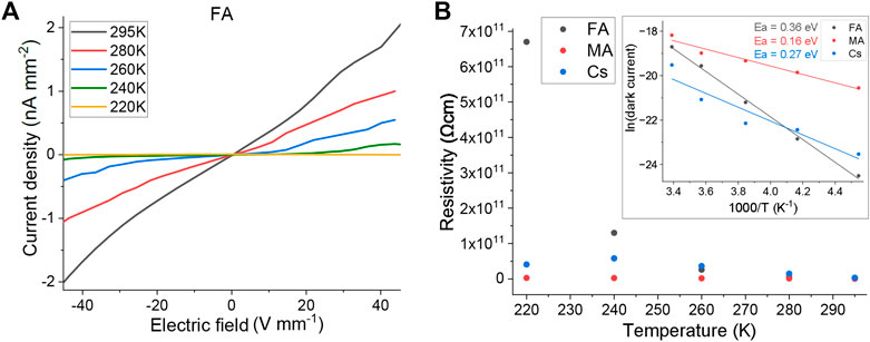
FIGURE 4. (A) I-V at low temperatures shows the reduction in dark current. (B) Consequential increasing resistivity at low temperatures, inset shows the Arrhenius plot with the extracted activation energies of 0.44 eV for FA, 0.16 eV for MA and 0.27 eV for Cs.
Activation energies were measured from the temperature-dependent currents, inset in Figure 4B). The physical interpretation of the activation energies is still open to debate; O’Kane et al. (2017) and Meloni et al. (2016) relate the activation energy to the energy of migrating ionic vacancies and Duijnstee et al. (2021) suggest that the activation energy is a combination of many different temperature dependent factors including trap density, ion density, carrier mobility, injection barrier from electrodes and ionisation of trapped carriers. In our data, since current hysteresis is suppressed, the activation energies extracted from dark current measurements may represent the energy difference of free and trapped charge carriers and are therefore related to the depth of traps which are active in the conductivity (Stallinga, 2009; Murdey and Sato, 2014).
To perform low temperature measurements the samples were placed under vacuum. However it was observed that the dark current of all three sample types increased under vacuum, shown in Figure 5A). To investigate this further the same experiment was carried out in dry oxygen gas, dry nitrogen gas and air, shown in Figure 5B), and the results were the same. This suggests that there are surface states which are passivated by O2, N2, and air and which influence the measured dark current. It has been widely reported that perovskite solar cell thin films degrade under vacuum due to out-gassing of the perovskite’s organic components (Guo et al., 2021; Jiang et al., 2020). However we do not anticipate significant levels of out-gassing from these bulk single crystals, and in our devices the dark current recovers once normal atmospheric pressure is achieved.
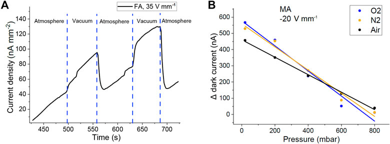
FIGURE 5. (A) Increasing dark current under vacuum for FA sample. (B) Difference in dark current between atmospheric pressure and stated pressure for MA sample in O2 gas, N2 gas or air. The same trends were observed for all 3 sample types.
3.2 X-ray sensitivity
The detector X-ray sensitivity is a key parameter for X-ray imaging devices, which are typically operated in photocurrent, or integrating, mode. Maximising the X-ray sensitivity is important to produce high contrast X-ray images, which can be acquired with a minimum X-ray dose rate. Of equal importance is the detector material dark current density, which determines both the minimum-detectable X-ray dose rate and also the ‘signal to noise’ on/off ratio of the X-ray signals.
Figure 6A) shows the on/off X-ray photocurrent response of the Cs, FA and MA devices, measured with a pulsed X-ray beam at a 100 ms pulse duration. The baseline photocurrent in each case represents the device dark current, which is higher in the MA sample (∼ 52 nA mm−2) compared to the lower dark currents of the FA and Cs devices (5–10 nA mm−2). The relative sensitivity of the devices can be observed from the height of the X-ray pulses, for which the FA device has the lowest sensitivity and the Cs device has the highest. Figure 6B) shows the variation in X-ray sensitivity as a function of electric field, with the Cs device reaching a maximum sensitivity of 4 µC mGy−1 cm−2 at a field strength of 30 V mm−1. Both the MA and Cs samples show a higher sensitivity under positive applied voltage, whereas the FA sample shows higher sensitivity under negative voltage.
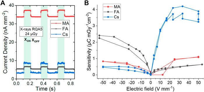
FIGURE 6. (A) X-ray photocurrent pulses for the Cs, MA and FA samples at electric field strength +50 V mm−1. The baseline signal represents the device dark current. (B) X-ray sensitivity against electric field strength for the 3 samples.
3.3 Drift mobility
Drift mobility was measured using a time of flight (ToF) method, with free carriers injected into the sample using either a pulsed 405 nm laser (FA, MA samples), or using 137Cs gamma rays (Cs sample). In order to minimise instabilities in the bulk electric field, a pulsed bias supply was used for the ToF measurements. Using this technique the bias voltage was only applied for a 10 ms window either side of the laser pulse. This suppressed ion migration and field distortion in the samples such that stable, reproducible ToF pulses were observed. For the FA and MA samples the metal contacts were 30 nm thick and therefore semi-transparent to the laser. The photon energy from the 405 nm laser was greater than the perovskite band-gap energy, and consequently the electron-hole pairs were created in the near-surface region directly under the top contact. By irradiating the laser pulses onto the anode (cathode) surface of the device, the current transients were observed solely from hole (electron) transport through the sample. For the Cs sample the thicker metal contact was not transparent to the laser pulses, so ToF was carried out using 662 keV gamma ray events from 137Cs. In this case the gamma interactions are distributed through the depth of the sample. Therefore gamma ray ToF data for the Cs sample measured a mean mobility due to both electron and hole transport.
Figure 7A) shows a set of ToF current pulses acquired from the FA sample using the 405 nm laser. The pulses show the inflection point due to the prompt charge drift, followed by a slower decay suggesting either dispersive or trap-related transport. This is consistent with previous reports of the dynamics of free charge carriers in metal halide perovskite single crystals, e.g., where the role of thermal carrier de-trapping in single crystal MAPbBr3 has been discussed by Musiienko et al. (2020). In order to further examine these effects we have used temperature-dependent analysis of alpha particle pulse shapes, described in Section 3.5.
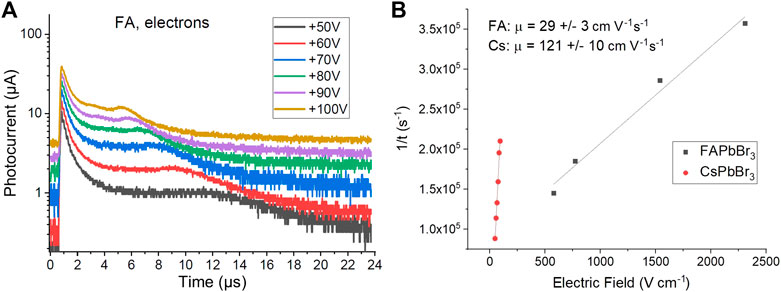
FIGURE 7. (A) Laser ToF current pulses from FA sample, showing the inflection point due to the prompt charge drift, together with some dispersive transport over longer times. The reduction in prompt transit times as a function of increasing bias can be observed, (B) Mobility graph for FA and Cs samples. For the FA sample the data shows electron mobility, for the Cs sample the data shows a mean mobility due to both electron and hole transport.
From the ToF current pulses the charge transit time was measured from the inflection point in the pulse shape, which moves to shorter times as the bias voltage is increased. For the 137Cs gamma ray ToF measurements on the Cs sample, the integrated charge ToF pulses were analysed using the pulse rise-time which represents the charge drift time (Zhang et al., 2021).
The reciprocal of the pulse transit time was plotted as a function of the applied electric field, and a linear fit to the data was used to measure the drift mobility. Two typical mobility plots from the FA and Cs samples are shown in Figure 7B).
Table 2 summarises the measured drift mobilities for these samples. For the FA and MA samples the drift mobilities were similar, although the FA samples consistently showed a higher electron mobility compared to holes. This is an unusual feature which we observe in all our FAPbBr3 samples, as generally the lead halides show a greater hole mobility compared to electrons (Liu et al., 2021). The mean mobility from the Bridgman-grown Cs sample was significantly higher than for the solution-grown FA and MA samples, consistent with previous reports by He et al. (2018).
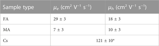
TABLE 2. Measured ToF drift mobilities for electrons and holes for FA, MA and Cs samples. *The mobility for Cs is a mean value for electrons and holes.
Table 3 summarises previously published drift mobility values for FA, MA and Cs lead bromide single crystals, which are broadly similar to our reported values. Results published for FA and MA samples are for solution-grown crystals, whilst values for Cs samples are for Bridgman-grown crystals. Published values contain a range of mobilities due to differences in sample quality and device performance. Table 3 only shows mobility values measured using ToF methods, and we exclude mobility values measured by the space-charge-limited-current (SCLC) method from I-V data using the Mott-Gurney equation. Although widely used for mobility estimates in perovskite thin films, the SCLC method has significant shortcomings when applied to mobility measurements in perovskite single crystals (Le Corre et al., 2021), e.g., the ability to correctly identify the Mott-Gurney region in the I-V data, and also the additional current contribution from slow ionic conductivity of either the A-site cation or the halide anions. The variation in mobility values obtained using ToF and SCLC methods can be seen in reported values of the hole mobility of FAPbBr3 single crystals ranging from μh = 0.12 cm2 V−1 s−1 using the SCLC method (Ng and Halpert, 2020) to μh = 61 cm2 V−1 s−1 using ToF (Zhumekenov et al., 2016).
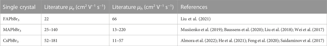
TABLE 3. Published electron and hole mobility ranges for FAPbBr3, MAPbBr3 and CsPbBr3 single crystals. Mobility values derived from space-charge-limited-current measurements were not included.
The time evolution of ToF current pulses also gives valuable insights into the electric field distribution within the crystal, since the induced current in the detector electrodes is proportional to the instantaneous drift velocity of the charge carriers. Therefore the time evolution of the ToF current pulses probes the internal electric field distribution as a function of the depth of the single crystal. Figure 8 shows ToF current pulses for hole and electron transport from the MA sample. Consistent differences can be seen in the shape of the current transients for electons and holes: for the electron transport the pulse signal reduces over time, whereas for the hole pulses the signal amplitude increases. This increase in signal amplitude as the charges drift through the detector is consistent with similar reports for MA samples (Baussens et al., 2020) and is attributed to a non-uniform electric field distribution in the MA device.
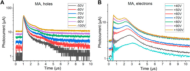
FIGURE 8. MA ToF response for (A) holes and (B) electrons, with electrons showing an increasing photocurrent as charges move towards the electrode.
The use of a pulsed bias voltage during ToF measurements limits ionic mobility and maintains the stability of the electric field within the crystal over long periods of time. If the bias voltage is applied permanently the pulse shapes are seen to change shape over the timescale of minutes, indicative of time-dependent changes to the internal field within the crystal. Figure 9 displays laser ToF current waveforms from typical FA and MA samples studied over a period of 10 minutes with constant applied bias. The observed waveforms reduce in amplitude and duration during this time, consistent with a reduction in the internal electric field distribution within the crystal. A possible mechanism for the reduction in the internal electric field over time may be due to ion migration in the crystals causing an opposing internal field.
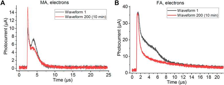
FIGURE 9. Typical laser ToF pulses under a constant bias of ±90 V applied for up to 10 minutes for (A) MA, and (B) FA samples. When the bias is applied continuously, changes in the ToF current pulses are observed consistent with modification of the internal electric field.
3.4 Alpha spectra and charge transport
3.4.1 Mobility-lifetime (μτ) measurements
Alpha spectroscopy using an 241Am source was carried out to investigate the mobility-lifetime products and charge drift lengths of the devices. Using an alpha particle pulse height spectrum the mobility-lifetime product μτ can be extracted by plotting the position of the alpha peak centroid as a function of bias. Due to the shallow interaction depth of alpha particles (approximately 20 μm in perovskite) the pulses are caused by electron (hole) transport if the alpha particles are incident on the cathode (anode) contact. This data is then fitted to the single carrier Hecht equation, below.
where A is a scaling factor based on the charge calibration, V is the applied bias and d is the sample thickness.
Figure 10 shows hole transport alpha spectra measured from three MA samples of different thicknesses, all acquired with the same electric field of 20 V mm−1. The thinner samples produce alpha-peaks with higher channel numbers, indicating that the holes are drifting over a significant fraction of the total device thickness. For the thickest sample MA3 the alpha peak has the lowest channel number, consistent with the average carrier drift length being significantly less than the device thickness of 1.49 mm. This data confirms that the mean charge drift lengths, at this field strength, are less than the device thickness and consistent with a relatively low μτ value (i.e., μτ < 8x10⁻⁴ cm2 V−1).
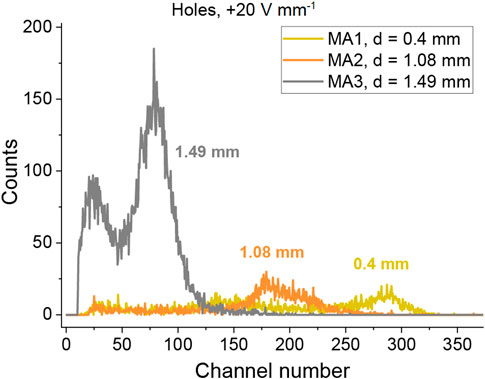
FIGURE 10. Hole transport alpha spectra of three MA samples of thicknesses 0.4 mm, 1.08 mm and 1.49 mm at an electric field strength of 20 V mm−1.
Well-resolved alpha peaks from FA electron transport can be seen in Figure 11A), where the peak centroid channel number increases with bias voltage. Similar alpha peaks were also observed for FA hole transport, and Figure 11B) shows the corresponding Hecht plots and calculated electron and hole μτ products. The electron μτe product was measured as 1 × 10⁻³ cm2 V−1, slightly higher than that for holes, μτh = 3 × 10⁻⁴ cm2 V−1.
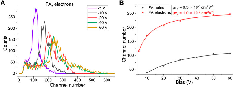
FIGURE 11. (A) Alpha spectra for electron transport in a FA sample (thickness = 1.8 mm), showing well resolved alpha peaks at various biases. (B) Hecht plots for FA electron and hole transport, with the corresponding μτ values.
In general the MA and Cs samples showed better-resolved alpha peaks from hole transport, which is the opposite compared to the FA samples. Figure 12 shows alpha spectra for hole transport in a Cs sample. In all cases the alpha spectra were acquired with the same gain, and the higher channel numbers observed from the Cs hole spectra indicate longer carrier drift lengths compared to the FA and MA samples. However for the Cs sample electron transport it was not possible to obtain well-resolved alpha peaks for electrons, consistent with reduced electron transport in CsPbBr3 as previously reported in (He et al., 2019). This is further confirmed by the alpha pulse shape measurements in the following section.
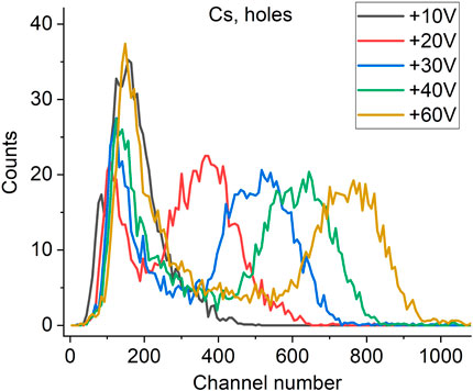
FIGURE 12. Alpha spectroscopy from hole transport of a Cs sample (thickness = 1.4 mm) at various applied biases.
The calculated μτ products for electrons and holes of all three sample types are tabulated in Table 4, together with previously reported literature values acquired from α-particle measurements. The published results reported in Table 4 exclude μτ values obtained from X-ray or optical photocurrent measurements, which tend to report artificially high values. The reason that photocurrent measurements tend to give high μτ values is not well understood, but is possibly due to the high rate of charge injection causing trap passivation in the perovskite.
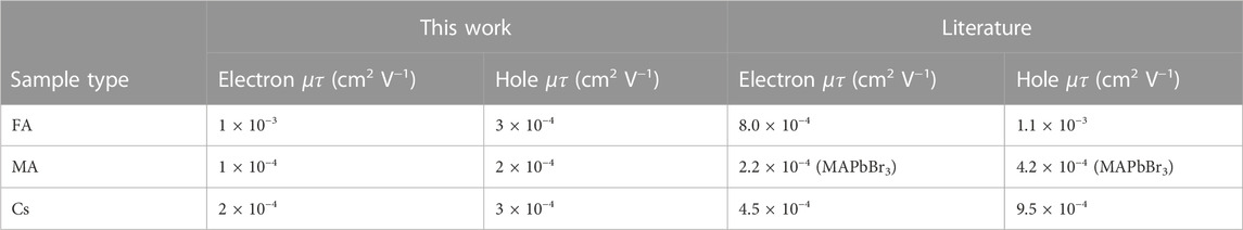
TABLE 4. Electron and hole mobility-lifetime products (μτ) for FA, MA and Cs samples. Mobility-lifetimes were extracted from alpha spectra using the single carrier Hecht Eq. 1. All literature values are for α-particle response of Am-241 and obtained from: FA (Liu et al., 2021), MA (Liu et al., 2018), Cs (He et al., 2019).
3.4.2 Pulse risetimes
Analysis of alpha pulse risetimes can give insights into the charge transport and carrier dynamics. Alpha pulses were acquired from the output of the charge-integrating preamplifier using a high speed waveform digitizer. Off-line analysis of the event-by-event pulse file was used to analyse the pulses, where the pulse risetime corresponds to the charge drift time in the device. Figures 13A, C, E show typical electron and hole pulse shapes from the FA, MA and Cs devices. For each recorded pulse the amplitude and risetime were measured. Some pulse shapes showed an initial fast risetime corresponding to the carrier drift, followed by a slow risetime component corresponding to trapping/detrapping and/or dispersive charge transport (Wang et al., 2006).
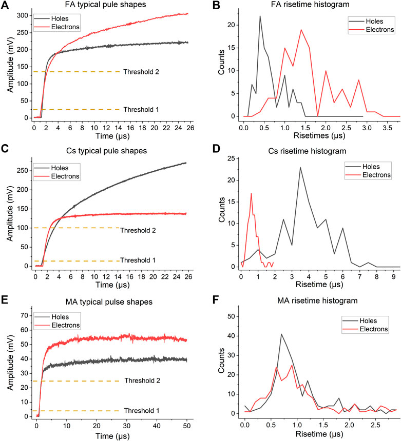
FIGURE 13. Electrons and holes in FA, Cs and MA samples where (A), (C), (E) show typical alpha pulse shapes and (B), (D), (F) show prompt risetime histograms. Threshold 1 and 2 cuts are 5% and 50% respectively for prompt risetime analysis and 5% and 90% respectively for long risetime analysis.
Histograms were produced for the energy and risetime parameters by analysing 300 pulse shapes from each device. Pulse risetimes were measured from the prompt region of the pulse, using amplitude threshold cuts at 5% and 50% of the pulse amplitude. Risetime comparisons are made between the different sample types in Figures 13B, D, F. For the Cs sample a disparity can be seen between electron and hole transport, where the hole risetimes are significantly longer than the electron risetimes. This is indicative of the strong slow component in the hole pulses and a long effective hole lifetime, which is not observed for the electron pulses. As a consequence the hole pulse amplitudes are greater than for electrons, consistent with hole transport dominating in the Cs samples. The pulse shape amplitudes and risetimes for the FA sample have the reversed trend, where the electron pulses have higher amplitudes and longer risetimes than the holes. By contrast, the MA sample shows very similar behaviour for the electron and hole risetimes.
Comparing the typical pulse shapes in Figures 13A, C, E, it can be seen that FA electrons and Cs holes have longer risetimes, suggesting that they are more susceptible to trapping and detrapping. The long risetime for FA electrons is approximately 10 μs, and for Cs holes it is approximately 20 μs, which generally agree with the transit times of the laser ToF results in Figure 7.
3.5 Low temperature charge transport
Low temperature measurements were carried out to investigate the potential influence of thermal trapping and de-trapping mechanisms on the charge tranport (Wang et al., 2006). Low temperature measurements were limited to 260 K to avoid the cubic-tetragonal phase change in FAPbBr3, as summarised in Table 1.
Drift mobility was measured for the different samples at room temperature and 260 K using ToF, as shown in Figure 14. Electron drift mobility in the FA sample showed a slight increase at 260 K, increasing from 29 cm2 V −1 s −1 at 295 K to 36 cm2 V −1 s −1 at 260 K. A similar trend was also observed for the MA and Cs samples, however the changes in drift mobility over this limited temperature range were not large.
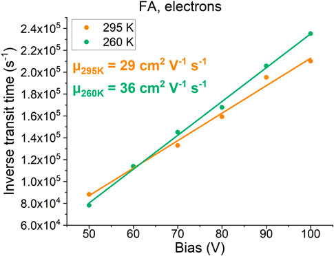
FIGURE 14. Electron mobility of FA sample measured using laser ToF, comparing 295 K and 260 K.
Similarly, alpha spectra at 260 K for FA electrons maintained well resolved alpha peaks and did not show a significant difference in shape compared to room temperature. The mobility-lifetime product slightly decreased at lower temperature, as shown in the corresponding Hecht plots in Figure 15 with a mobility-lifetime product (μτ260K = 5 × 10⁻⁴ cm2 V−1 s−1) measured at 260 K. Similar small changes in mobility-lifetime product were also observed in the MA and Cs samples, shown in Table 5.
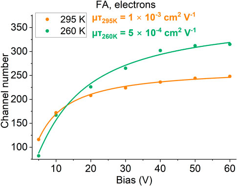
FIGURE 15. Hecht plots extracted from alpha peaks of electron transport in FA, comparing 295 K and 260 K.
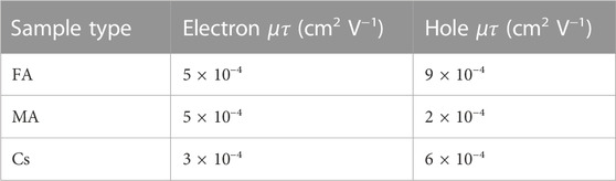
TABLE 5. Measured low temperature mobility-lifetime products (μτ) at 260 K
Overall no major changes were observed in the pulse risetimes for all 3 samples at low temperature. This result suggests that thermally-activated trapping/de-trapping charge transport is not dominant over the temperature range studied. Further studies are required to analyse pulse risetimes are temperatures below 260 K to see if charge trapping effects become stronger at lower temperatures.
3.6 Gamma spectroscopy
For gamma ray spectroscopy, unlike with alpha particles, gamma rays create electron-hole pairs throughout the depth of the sample, so gamma events generally involve both electron and hole transport in the device. As the energy deposition from gamma events is significantly less than for alpha particles, the measurement requires a low noise system to obtain good gamma spectra.
The relatively long shaping time of 10 μs used for perovskite measurements, due to their low mobility, has a significant effect on the electronic noise and the spectral resolution. We studied how the device leakage current influenced the position of the noise edge in a gamma pulse height spectrum. Figure 16 compares the noise edge channel number recorded in a pulse height spectrum as a function of increasing shaping time, acquired using a digital shaping amplifier. Two perovskite devices are shown, one with a leakage current of 0.04 μA, and a second with a leakage current of
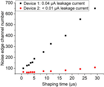
FIGURE 16. Noise edge as a function of shaping time for devices with different leakage currents, i.e.,
In our thick planar perovskite devices a resolved gamma peak was not observed. This was mainly due to the low and unequal mobility-lifetime products for electrons and holes in these samples. Figure 17 shows the gamma spectra obtained from an FA sample using Am-241 (59 keV), Co-57 (122 keV) and Cs-137 (662 keV) sources. Using the maximum channel number for each spectrum, the energy calibration (inset) showed a linear response.
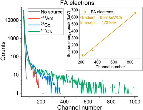
FIGURE 17. Gamma spectra using FA sample, with sources Am-241 (59 keV peak), Co-57 (122 keV peak) and Cs-137 (662 keV peak), shaping time = 5.1 μs. Inset shows calibration plot.
Previous reports of perovskite gamma ray spectra have achieved a well-resolved full energy peak using a CsPbBr3 single crystal with planar GaIn/CsPbBr3/Au contacts, achieving a FWHM energy resolution of 1.4% with Cs-137 (662 keV) (He et al., 2021). This performance was achieved due to the very high quality crystal used in the study. Further improvements in the gamma resolution have also been achieved when using unipolar charge sensing schemes, such as the small pixel effect, to minimise charge trapping in the device.
For solution-grown metal halides, an energy resolution of 6.5% FWHM at 662 keV was reported for MAPbBr2.94Cl0.06 single crystal using Cr/MAPbBr2.94Cl0.06/C60/bathocuproine/Cr contacts with a guard ring (Wei et al., 2017). A low energy resolved gamma peak was reported for FAPbBr3 with a resolution of 40.1% FWHM using planar Au/FAPbBr3/Au contacts (Liu et al., 2021). In all cases a key requirement for gamma spectroscopy is for the perovskite device to be stable under high bias voltages, whilst maintaining a very low dark current.
4 Conclusion
We have reported a comparative study of charge transport and radiation detector performance of FA, MA and Cs based lead bromide single crystals. Crucial for operation as a radiation detector is the stability of the device under high applied bias voltages, and the minimisation of dark current. All the samples studied showed bulk resistivity values in the range 2 × 10⁹ Ωcm–2 × 10¹⁰ and it was observed that the surface preparation of the samples strongly affected the measured dark current.
Laser ToF pulses were observed for all sample types with the pulse shapes showing both prompt and delayed charge transport. Uniquely, the MA sample showed a non-uniform, increasing electric field. It was also observed that the internal field changed with time under an applied constant bias for the FA and MA samples, suggesting the build-up of internal opposing charges. Unstable and non-uniform (i.e., from anode to cathode, or vice versa) internal electric fields are potentially significant as they could affect device performance. Further studies are required to mitigate these field stability effects, such as through improved crystal quality or optimized metal-perovskite contacts.
The samples show well resolved alpha peaks, and alpha pulse shape analysis was used to confirm the role of prompt and dispersive charge transport. Cs samples showed a higher drift mobility, for holes, compared to the solution-grown FA and MA samples, and also showed least sensitivity to internal field instability. Low temperature measurements were used to reduce the dark current and to measure the dark current activation energies, however there was no significant change observed in drift mobilities at low temperatures, down to 260 K.
It was observed that one of the key limiting factors for high detection sensitivity and good energy resolution is the presence of dark current. This is exacerbated by the need to operate perovskite devices with long shaping times, due to the relatively low carrier drift velocities. Based on our study, the charge transport performance and detector response of Bridgman-grown CsPbBr3 is currently superior to the solution grown lead halides, however both FAPbBr3 and MAPbBr3 show promise for future detector applications.
Data availability statement
The raw data supporting the conclusion of this article will be made available by the authors, without undue reservation.
Author contributions
Data analysis and manuscript preparation was carried out by SB and PS. All authors contributed to the article and approved the submitted version.
Funding
This work was funded by the US Defense Threat Reduction Agency under Basic Research contract HDTRA1-18-1-0019, and also through the DTRA Interaction of Ionizing Radiation with Matter University Research Alliance (IIRM-URA) under contract number HDTRA1-20-2-0002. The project or effort depicted was or is sponsored by the Department of the Defense, Defense Threat Reduction Agency. The content of the information does not necessarily reflect the position or the policy of the federal government, and no official endorsement should be inferred. This work has also has received funding from the European Union’s Horizon 2020 research and innovation program under the Photonics Public Private Partnership (www.photonics21.org) with the project PEROXIS under Grant Agreement No. 871336. The work at Argonne National Laboratory was supported by the Department of Energy, National Nuclear Security Administration, Office of Defense Nuclear Nonproliferation Research and Development under Contract No. DEAC02-06CH11357 and the Department of Energy, Basic Energy Sciences (for exploration of Hi-Z detector materials for synchrotron detector applications).
Conflict of interest
MK and DC are co-founders of Actinia Inc, a company that applies perovskite materials to radiation detection.
The remaining authors declare that the research was conducted in the absence of any commercial or financial relationships that could be construed as a potential conflict of interest.
The author PS declared that they were an editorial board member of Frontiers, at the time of submission. This had no impact on the peer review process and the final decision.
Publisher’s note
All claims expressed in this article are solely those of the authors and do not necessarily represent those of their affiliated organizations, or those of the publisher, the editors and the reviewers. Any product that may be evaluated in this article, or claim that may be made by its manufacturer, is not guaranteed or endorsed by the publisher.
Supplementary material
The Supplementary Material for this article can be found online at: https://www.frontiersin.org/articles/10.3389/fdest.2023.1249892/full#supplementary-material
References
Almora, O., Matt, G. J., These, A., Kanak, A., Levchuk, I., Shrestha, S., et al. (2022). Surface versus bulk currents and ionic space-charge effects in cspbbr3 single crystals. J. Phys. Chem. Lett. 13 (17), 3824–3830. doi:10.1021/acs.jpclett.2c00804
Baussens, O., Maturana, L., Amari, S., Zaccaro, J., Verilhac, J.-M., Hirsch, L., et al. (2020). An insight into the charge carriers transport properties and electric field distribution of ch3nh3pbbr3 thick single crystals. Appl. Phys. Lett. 117 (4), 041904. doi:10.1063/5.0011713
Duijnstee, E. A., Le Corre, V. M., Johnston, M. B., Koster, L. J. A., Lim, J., and Snaith, H. J. (2021). Understanding dark current-voltage characteristics in metal-halide perovskite single crystals. Phys. Rev. Appl. 15 (1), 014006. doi:10.1103/physrevapplied.15.014006
Feng, Y., Pan, L., Wei, H., Liu, Y., Ni, Z., Zhao, J., et al. (2020). Low defects density cspbbr 3 single crystals grown by an additive assisted method for gamma-ray detection. J. Mater. Chem. C 8 (33), 11360–11368. doi:10.1039/d0tc02706e
Guo, R., Han, D., Chen, W., Dai, L., Ji, K., Xiong, Q., et al. (2021). Degradation mechanisms of perovskite solar cells under vacuum and one atmosphere of nitrogen. Nat. Energy 6 (10), 977–986. doi:10.1038/s41560-021-00912-8
He, Y., Liu, Z., McCall, K. M., Lin, W., Chung, D. Y., Wessels, B. W., et al. (2019). Perovskite cspbbr3 single crystal detector for alpha-particle spectroscopy. Nucl. Instrum. Methods Phys. Res. Sect. A Accel. Spectrom. Detect. Assoc. Equip. 922, 217–221. doi:10.1016/j.nima.2019.01.008
He, Y., Matei, L., Jung, H. J., McCall, K., Chen, M., Stoumpos, C., et al. (2018). High spectral resolution of gamma-rays at room temperature by perovskite cspbbr3 single crystals. Nat. Commun. 9, 1609. doi:10.1038/s41467-018-04073-3
He, Y., Petryk, M., Liu, Z., Chica, D. G., Hadar, I., Leak, C., et al. (2021). Cspbbr3 perovskite detectors with 1.4% energy resolution for high-energy γ-rays. Nat. Photonics 15 (1), 36–42. doi:10.1038/s41566-020-00727-1
Jiang, Y., Yang, S.-C., Jeangros, Q., Pisoni, S., Moser, T., Buecheler, S., et al. (2020). Mitigation of vacuum and illumination-induced degradation in perovskite solar cells by structure engineering. Joule 4 (5), 1087–1103. doi:10.1016/j.joule.2020.03.017
Keshavarz, M., Ottesen, M., Wiedmann, S., Wharmby, M., Küchler, R., Yuan, H., et al. (2019). Tracking structural phase transitions in lead-halide perovskites by means of thermal expansion. Adv. Mater. 31 (24), 1900521. doi:10.1002/adma.201900521
Le Corre, V. M., Duijnstee, E. A., El Tambouli, O., Ball, J. M., Snaith, H. J., Lim, J., et al. (2021). Revealing charge carrier mobility and defect densities in metal halide perovskites via space-charge-limited current measurements. ACS energy Lett. 6 (3), 1087–1094. doi:10.1021/acsenergylett.0c02599
Liu, X., Xu, M., Hao, Y., Fu, J., Wang, F., Zhang, B., et al. (2021). Solution-grown formamidinium hybrid perovskite single crystals for α-particle and γ-ray detection at room temperature. ACS Appl. Mater. Interfaces 13 (13), 15383–15390. doi:10.1021/acsami.1c00174
Liu, X., Zhang, H., Zhang, B., Dong, J., Jie, W., and Xu, Y. (2018). Charge transport behavior in solution-grown methylammonium lead tribromide perovskite single crystal using α particles. J. Phys. Chem. C 122 (26), 14355–14361. doi:10.1021/acs.jpcc.8b03512
Mayen Guillén, J., Lédée, F., Baussens, O., Chapran, M., Lemercier, T., Verilhac, J. M., et al. (2023). Mapb(br1−xclx)3 hybrid perovskite materials for direct x-ray detection. ACS Appl. Electron. Mater. 5, 1866–1878. doi:10.1021/acsaelm.3c00114
Meloni, S., Moehl, T., Tress, W., Franckevičius, M., Saliba, M., Lee, Y. H., et al. (2016). Ionic polarization-induced current–voltage hysteresis in ch3nh3pbx3 perovskite solar cells. Nat. Commun. 7 (1), 10334–10339. doi:10.1038/ncomms10334
Murdey, R., and Sato, N. (2014). Interpretation of the thermal activation energy of conduction for molecular semiconductor thin films with blocking contacts. Jpn. J. Appl. Phys. 53 (5), 05FY04. doi:10.7567/jjap.53.05fy04
Musiienko, A., Moravec, P., Grill, R., Praus, P., Vasylchenko, I., Pekarek, J., et al. (2019). Deep levels, charge transport and mixed conductivity in organometallic halide perovskites. Energy & Environ. Sci. 12 (4), 1413–1425. doi:10.1039/c9ee00311h
Musiienko, A., Pipek, J., Praus, P., Brynza, M., Belas, E., Dryzhakov, B., et al. (2020). Deciphering the effect of traps on electronic charge transport properties of methylammonium lead tribromide perovskite. Sci. Adv. 6 (37), eabb6393. doi:10.1126/sciadv.abb6393
Ng, M., and Halpert, J. E. (2020). Single crystals of mixed br/cl and sn-doped formamidinium lead halide perovskites via inverse temperature crystallization. RSC Adv. 10 (7), 3832–3836. doi:10.1039/d0ra00060d
O’Kane, S. E., Richardson, G., Pockett, A., Niemann, R. G., Cave, J. M., Sakai, N., et al. (2017). Measurement and modelling of dark current decay transients in perovskite solar cells. J. Mater. Chem, 5 (2), 452–462. doi:10.1039/c6tc04964h
Poludniowski, G. G., and Evans, P. M. (2007a). Calculation of x-ray spectra emerging from an x-ray tube. part i. electron penetration characteristics in x-ray targets. Med. Phys. 34, 2164–2174. doi:10.1118/1.2734725
Poludniowski, G. G., and Evans, P. M. (2007b). Calculation of x-ray spectra emerging from an x-ray tube. part ii. x-ray production and filtration in x-ray targets. Med. Phys. 34, 2175–2186. doi:10.1118/1.2734726
Rosado, P. H. G., Nogueira, M. d. S., and Oliveira, P. M. C. “Determination of the mean energy for attenuated and unattenuated iec diagmostic x-ray beams,” in Proc. of 2007 International Nuclear Atlantic Conference - INAC 2007, Santos, SP, Brazil, September 2007,
Saidaminov, M. I., Haque, M. A., Almutlaq, J., Sarmah, S., Miao, X.-H., Begum, R., et al. (2017). Inorganic lead halide perovskite single crystals: phase-selective low-temperature growth, carrier transport properties, and self-powered photodetection. Adv. Opt. Mater. 5 (2), 1600704. doi:10.1002/adom.201600704
Schueller, E. C., Laurita, G., Fabini, D. H., Stoumpos, C. C., Kanatzidis, M. G., and Seshadri, R. (2018). Crystal structure evolution and notable thermal expansion in hybrid perovskites formamidinium tin iodide and formamidinium lead bromide. Inorg. Chem. 57 (2), 695–701. doi:10.1021/acs.inorgchem.7b02576
Sellin, P., and Vaitkus, J. (2006). New materials for radiation hard semiconductor dectectors. Nucl. Instrum. Methods Phys. Res. Sect. A Accel. Spectrom. Detect. Assoc. Equip. 557, 479–489. doi:10.1016/j.nima.2005.10.128
Stallinga, P. (2009). Electrical characterization of organic electronic materials and devices. Hoboken, New Jersey, United States: John Wiley & Sons.
Wang, J., Zhang, J., Zhou, Y., Liu, H., Xue, Q., Li, X., et al. (2020). Highly efficient all-inorganic perovskite solar cells with suppressed non-radiative recombination by a lewis base. Nat. Commun. 11 (1), 177–179. doi:10.1038/s41467-019-13909-5
Wang, S., Sellin, P., and Lohstroh, A. (2006). Temperature-dependent hole detrapping for unprimed polycrystalline chemical vapor deposited diamond. Appl. Phys. Lett. 88 (2), 023501. doi:10.1063/1.2162673
Wei, H., DeSantis, D., Wei, W., Deng, Y., Guo, D., Savenije, T. J., et al. (2017). Dopant compensation in alloyed ch3nh3pbbr3-xclx perovskite single crystals for gamma-ray spectroscopy. Nat. Mater. 16 (8), 826–833. doi:10.1038/nmat4927
Whitcher, T., Gomes, L., Zhao, D., Bosman, M., Chi, X., Wang, Y., et al. (2019). Dual phases of crystalline and electronic structures in the nanocrystalline perovskite cspbbr3. NPG Asia Mater. 11 (1), 70–12. doi:10.1038/s41427-019-0170-6
Yakunin, S., Dirin, D. N., Shynkarenko, Y., Morad, V., Cherniukh, I., Nazarenko, O., et al. (2016). Detection of gamma photons using solution-grown single crystals of hybrid lead halide perovskites. Nat. Photonics 10 (9), 585–589. doi:10.1038/nphoton.2016.139
Zhang, B.-B., Wang, F., Liu, X., Xiao, B., Xu, M., Dong, S.-T., et al. (2021). Ion migration controlled stability in - particle response of cspbbr2.4cl0.6 detectors. J. Phys. Chem. C 125, 4235–4242. doi:10.1021/acs.jpcc.0c10758
Zhang, F., Yang, B., Zheng, K., Yang, S., Li, Y., Deng, W., et al. (2018). Formamidinium lead bromide (fapbbr3) perovskite microcrystals for sensitive and fast photodetectors. Nano-micro Lett. 10 (3), 43–48. doi:10.1007/s40820-018-0196-2
Keywords: perovskite, radiation detector, charge transport, X-ray, gamma ray
Citation: Bennett SH, Ghosh J, Gros-Daillon E, Lédée F, Mayén Guillén J, Verilhac J-M, Zaccaro J, Chung DY, Klepov V, Kanatzidis MG and Sellin PJ (2023) Charge transport comparison of FA, MA and Cs lead halide perovskite single crystals for radiation detection. Front. Detect. Sci. Technol 1:1249892. doi: 10.3389/fdest.2023.1249892
Received: 29 June 2023; Accepted: 24 August 2023;
Published: 14 September 2023.
Edited by:
M. Zahangir Kabir, Concordia University, CanadaReviewed by:
Safa Kasap, University of Saskatchewan, CanadaMatti Kalliokoski, University of Helsinki, Finland
Olivier Tousignant, Teledyne Dalsa, Netherlands
Copyright © 2023 Bennett, Ghosh, Gros-Daillon, Lédée, Mayén Guillén, Verilhac, Zaccaro, Chung, Klepov, Kanatzidis and Sellin. This is an open-access article distributed under the terms of the Creative Commons Attribution License (CC BY). The use, distribution or reproduction in other forums is permitted, provided the original author(s) and the copyright owner(s) are credited and that the original publication in this journal is cited, in accordance with accepted academic practice. No use, distribution or reproduction is permitted which does not comply with these terms.
*Correspondence: Paul J. Sellin, p.sellin@surrey.ac.uk