Investigating binding energies and trapping cross-sections in an n-type Ge detector at low temperatures
 Sanjay Bhattarai
  Dongming Mei
- Department of Physics, The University of South Dakota, Vermillion, SD, United States
We investigated charge transport in an n-type germanium detector at 5.2 K to explore new technology for enhancing low-mass dark matter detection sensitivity. Calculations of dipole and cluster dipole state binding energies and electric field-dependent trapping cross-sections are critical to developing low-threshold detectors. The detector operates in two methods: depleting at 77K before cooling, or directly cooling to 5.2 K and applying different bias voltages. Results indicated lower binding energy of charge states in the second method, at zero field and under an electric field, suggesting different charge states formed under different operating methods. Measured cluster dipole and dipole state binding energies at zero field were 7.88± 0.64 meV and 8.37± 0.75 meV, respectively, signifying high low-threshold potential for low-mass dark matter searches in the future.
1 Introduction
The interaction between dark matter (DM) and ordinary matter is limited to weak elastic scattering processes, resulting in only a small energy deposition from nuclear or electron recoil (Ahmed et al., 2011; Armengaud et al., 2012; Zhao et al., 2013). This highlights the need for a detector with a very low energy threshold to detect DM (Mei et al., 2018). The LZ experiment has pushed the sensitivity for weakly interacting massive particles (WIMPs) with a mass greater than 10 GeV/c2 to the point where the neutrino-induced background limits its sensitivity (Aalbers et al., 2022). However, the recent emergence of low-mass DM in the MeV range has generated excitement as a DM candidate, although current experiments cannot detect it due to its small mass (Essig et al., 2012; Hochberg et al., 2016; Agnese et al., 2018; Arnaud et al., 2020; Al Kharusi et al., 2023; Berghaus et al., 2023). The detection of MeV-scale DM requires new detectors with thresholds as low as sub-eV, since both electronic and nuclear recoils from MeV-scale DM range from sub-eV to 100 eV (Essig et al., 2012). Conventional detector techniques cannot detect this low-mass DM.
Germanium (Ge) detectors have the lowest energy threshold among any current detector technology, making them ideal for low-mass DM searches (Armengaud et al., 2012; Agnese et al., 2014; Armengaud et al., 2018; Agnese et al., 2019). The band gap of Ge at 77K is 0.7 eV and the average energy required to generate an electron-hole pair in Ge is about 3 eV (Wei and Mei, 2017). Thus, a Ge detector can provide a very low energy threshold. Furthermore, proper doping of the Ge detector with impurities can expand the parameter space for low-mass DM searches even further. Shallow-level impurities in Ge detectors have binding energies of about 0.01 eV, and can form dipole states and cluster dipole states when operated at temperatures below 10K (Mei et al., 2018; Bhattarai et al., 2021; Mei et al., 2022). These dipole states and cluster dipole states have even lower binding energies than the impurities themselves, providing a potential avenue for detecting low-mass DM. Although the binding energies of impurities in Ge is well understood (Vénos et al., 2000; Sundqvist et al., 2009), little is known about the binding energy of the dipole states and cluster dipole states near helium temperature.
At low temperatures near liquid helium, residual impurities in germanium freeze out from the conduction or valence band into localized states, forming electric dipoles (
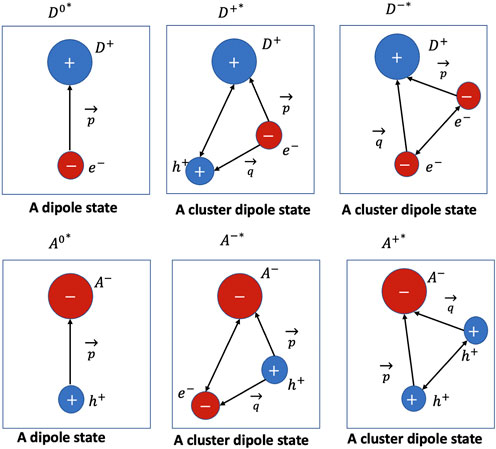
FIGURE 1. The mechanisms involved in the formation of dipole states and cluster dipole states in an n-type (upper) and p-type (lower) Ge detector operating at temperatures around 5 K, where
2 Experimental procedure
The USD crystal growth and detector development infrastructure is a state-of-the-art facility equipped with a zone refining process for purifying commercial ingots to a high level of purity suitable for crystal growth using the Czochralski method (Wang et al., 2012; Yang et al., 2014; Raut et al., 2020). This results in high-quality homegrown crystals that are used for the fabrication of n-type (R09-02) detectors in the USD detector fabrication lab (Panth et al., 2022). The R09-02 detector has a net impurity concentration of 7.02 × 10¹⁰/cm3 and dimensions of 11.7 mm × 11.5 mm × 5.5 mm. We employed the van der Pauw Hall Effect measurement technique to determine and characterize both the net carrier concentration and the material type of our selected samples. The Hall voltage across the sample is one of the most basic parameters we measure. The net carrier concentration and carrier type were derived from the Hall coefficient, which shows a linear relationship with the applied magnetic field. Furthermore, the longitudinal resistivity measurements enabled us to calculate the conductivity and Hall mobility.In our sample preparation process, we utilized an etchant consisting of a 1:4 mixture of hydrofluoric acid and nitric acid. This etchant was applied to samples cut from a crystal grown at USD, with an etching duration of three to 4 min, effectively eliminating surface imperfections and yielding a smooth and homogeneous surface. To establish Ohmic connections, we employed Gallium Indium eutectic, connecting it to the four corners of the samples, all of which were p-type. Subsequently, we subjected these van der Pauw samples to a heat treatment at 360°C for 30 min, allowing the Ge sample to properly absorb the Gallium Indium eutectic. Our measurements were conducted one sample at a time using the Ecopia HMS-3000 Hall Effect apparatus, complemented by a permanent magnet generating a field strength of 0.55 T. These measurements were performed at a liquid nitrogen temperature of 77 K. In accordance with the IEEE Standard, we determined the Hall mobility of the sample to be approximately 3.7 × 104 cm2/Vs, with a measurement uncertainty of 5%. Importantly, this value closely aligns with the IEEE Standard and is supported by prior research 239 (IEEE, 1993; Raut et al., 2020). The detector is mounted inside of a pulse tube refrigerator (PTR), which lowers its temperature from room temperature to almost liquid helium temperature. To provide accurate temperature readings, we installed two temperature sensors inside the cryostat. The first sensor is positioned at the bottom of a copper plate on which the detector rests on a thin sheet of indium foil, while the other sensor is positioned on top of another copper plate near the top surface of the detector. By sandwiching the detector between these two sensors, we can measure its temperature with a 0.5 K accuracy. The schematic diagram of the PTR is shown in Figure 2. To calibrate the detector, we utilized an Am-241 source and observed a distinct peak at 3.7 MeV under cryogenic conditions at 77 K. This energy peak served as our reference point for calculating the charge collection efficiency at various bias voltages. For each of these bias voltages, we calculated the mean energy by performing energy spectrum measurements at regular 2- to 3-min intervals over a 60-min duration. We subsequently conducted Gaussian fitting to determine the mean energy within each time interval, which was then plotted against time. We calculated the overall mean energy for each bias voltage by taking the average of these energies. To ascertain the charge collection efficiency at 5.2 K (as exemplified in 10 for different biases for method 1), we divided the mean energy obtained from the energy versus time plot by the reference energy of 3.7 MeV. Our set up of measurement electronics, used for characterizing the detectors, consists of a multimeter linked to a transimpedance amplifier, used in measuring leakage current. Additionally, we integrated signal processing electronics designed for precise signal readout. These signal readout electronics consisted of an AC-coupled charge-sensitive preamplifier, followed by a commercially available analog pulse-shaping amplifier. This configuration allowed us to not only undertake energy deposition measurement in the detector but also measure detector capacitance as a function of the applied detector voltage. To capture the energy spectrum effectively, we employed an ORTEC MCA (Multi-Channel Analyzer). A well labelled picture of the energy measurement system is shown in Figure 3. We calibrated alpha energy at 1800 V and 77.8 K, by observing the well-known gamma peak of 59.5 keV emitted by Am-241 as a steadfast reference point. Importantly, we adhered to this setup consistently throughout calibrations conducted at lower temperatures. As a part of our comprehensive testing procedure, we recorded the pulser peak, which served to understand the electronics noise level of the test system. Subsequently, we analyzed both the full width at half maximum (FWHM) of the 59.5 keV peak and the pulser peak, employing dedicated MCA software for examination and assessment.
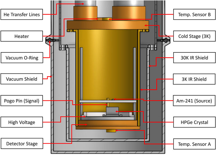
FIGURE 2. The labelled schematic diagram of the pulse tube refrigerator (PTR) used in this experiment for cooling down the detector R09-02 upto 5.2 K.
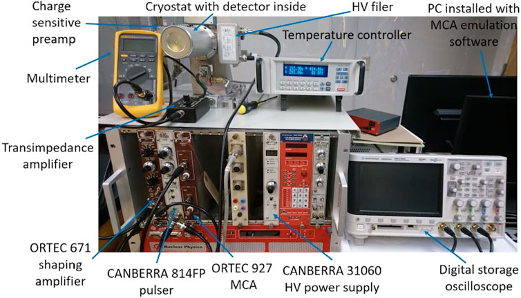
FIGURE 3. The labelled picture of the energy spectrum measurement system used in this experiment Wei et al. (2020).
Based on the capacitance measurements published in Ref Mei et al. (2022), we selected a working temperature of 5.2 K. The capacitance measurements show that at temperatures below 6.5 K, the capacitance is constant. We selected a working temperature of 5.2 K to guarantee that the capacitance is steady so that error can be minimized.
To ensure optimal electrical performance, an amorphous Ge passivation layer of 600 nm was coated on the surface of the Ge crystal as the electrical contact, effectively blocking surface charges (Wei et al., 2018; Bhattarai et al., 2020). An alpha source (241Am) was positioned near the detector inside a cryostat, and the energy deposition of α particles was measured. This creates localized electron-hole pairs near the top surface of the detector, and the electrons are drifted through the detector by applying a positive bias voltage to the bottom of the detector. The experimental setup for this measurement is illustrated in Figure 4.
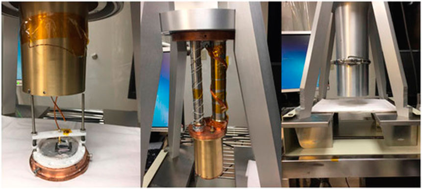
FIGURE 4. The detector is loaded into a pulse tube refrigerator (PTR), and two temperature sensors mounted above and below the detector are used to determine the temperature of the detector.
2.1 Method 1
In this method, an n-type planar detector is first cooled to 77K and a bias voltage is applied, gradually increasing until the detector is fully depleted at 1,200 V. The bias is then increased by an additional 600 V to become the operational voltage. The detector is then cooled down to 5.2 K while still under the applied operational voltage. The R09-02 detector used in this study, was depleted at 77 K with a depletion voltage of 1200 V and an operational voltage of 1800 V. An alpha source (241Am) emitting alpha particles with an energy of 5.3 MeV was positioned above the detector within the cryostat. The energy spectrum was measured for the energy deposition of the 5.3 MeV alpha particles, which was visible as a 3.7 MeV energy peak due to energy loss on the way to the detector’s active region. This 3.7 MeV energy deposition served as a reference for the energy deposition of 5.3 MeV alpha particles in the n-type detector without charge trapping, as the detector charge trapping at 77 K with a bias of 1800 V was negligible. The data were collected with a bias voltage applied in descending order from 1800 V to 30 V at 5.2 K, with histograms of energy deposition by alpha particles recorded every 2–3 min for 60 min at each bias voltage. The charge collection efficiency was determined by dividing the measured alpha energy peak by 3.7 MeV for a given bias voltage. At 77 K, the depletion process causes all the free charge carriers to be swept away, leaving only the space charge states, D+, behind. Upon cooling to 5.2 K, a charge trapping process occurs, resulting in the formation of dipole states as electrons drift across the detector (Mei et al., 2022). Continued drift of electrons across the detector can result in de-trapping of charge carrier through impact ionization of the dipole states (Mei et al., 2022). The key charge-trapping and de-trapping processes are described below:
In this method, the operation of the n-type planar detector begins with the formation of dipole states via charge trapping as a result of the Coulomb force between the space charge states and the drifting electrons at low fields. The second process is the release of trapped charge through impact ionization of the dipole states, known as charge de-trapping. In Method 1, when a positive bias voltage is applied, electrons are drifted across the detector, leading to the formation of dipole states
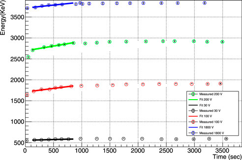
FIGURE 5. The mean energy deposition (Edep) versus time (t) for detector R09-02 in Method 1. As an example, the mean energy deposition (Edep) and time (t) recorded for a bias voltage of 200 V have been plotted for detector R09-02 when it is operated in Method 1. The error in Edep originates from the determination of energy deposition, while the error in t is primarily due to the determination of recorded time. A linear fit (Edep = p0 × t + p1) was applied to the portion of the plot where the emission of charge carriers is higher than the trapping of charge carriers. The slope (p0) of the fit was calculated to be 0.235 ± 0.025 and the intercept (p1) was 2687.09 ± 138.8. It is important to note that the slope represents the emission rate of charge (en) in Eq. 3.
2.2 Method 2
In this method of operation, the n-type planar Ge detector is cooled directly to 5.2 K without any applied bias voltage. Once cooled, the detector is then biased to the desired voltage level. At these low temperatures, impurities in the Ge crystal freeze out from the conduction or valence band to form localized states that result in the creation of dipole states. As it is an n-type detector, the majority of these dipole states are
The first process in this method is a trapping of charges by the Coulomb forces exerted by the dipole states on the drifted electrons, resulting in the formation of cluster dipole states. The second process is a de-trapping of charges through impact ionization of the cluster dipole states. The detector experiences a dynamic process of charge trapping, transport, and creation. The study of the time-dependent de-trapping of charges through the impact ionization of cluster dipole states helps us determine their binding energy.Once the temperature reached 5.2 K, a positive bias voltage was gradually applied from the bottom of the detector, causing the electrons created on the surface to be drifted across the detector under the electric field. Energy spectrum measurements were taken at different bias voltages of 30 V, 100 V, 200 V, 300 V, 450 V, 600 V, 1200 V, and 1800 V. Similar to Method 1, data were taken for 60 min at each bias voltage with histograms of energy deposition by alpha particles recorded every 2–3 min.
When comparing the two operational methods, it can be noted that in Method 2, the dipole states are formed at 5.2 K without any applied bias voltage. These dipole states rapidly trap charges as soon as the electrons are drifted across the detector, resulting in a shorter trapping time and lower binding energy. In contrast, in Method 1, the dipole states are formed in the space charge region when electrons are drifted across the detector with an applied bias voltage. Dipole states may exhibit significantly extended trapping periods due to their association with localized energy levels stemming from defects within the germanium crystal lattice. Additionally, the proximity of multiple charge carriers gives rise to cluster dipole states. This clustering enhances the effective density of dipole states and increases the likelihood of charge carriers encountering them. Consequently, charge carriers can be captured more efficiently in comparison to individual dipole states, leading to shorter trapping times. Therefore, it is expected that the trapping time can be longer and the binding energy of the dipole states will be higher than that of the cluster dipoles.
2.3 Physics model
If a positive bias voltage is applied to the bottom of the detector, electrons produced by the α particles from the 241Am source, which is located above the detector within the cryostat, can be drifted across the detector. This drifting of electrons leads to the formation of cluster dipole states,
where σtrap represents the trapping cross-section, vth is the thermal velocity, Nc = 2.46 × 10¹⁵/cm3 is the effective density of states of electrons in the conduction band at 5.2 K, EB is the binding energy of the trapped charge carriers, kB is the Boltzmann constant, and T is the temperature of the detector.
By using the experimental data to directly determine en and by knowing the values of vth (Mei et al., 2022), Nc (Conwell, 1955), and T, one can obtain the binding energy of dipole states or cluster dipole states from Eq. 3, provided the value of the trapping cross-section, σtrap, is known. However, determining the value of σtrap requires further calculation, as will be discussed.
The trapping cross-section (σtrap) of the charge carriers is related to the trapping length (λth) through the following relation: (Phipps, 2016; Mei et al., 2020):
where NA and ND represent the p-type and n-type impurities, respectively. vtot is the total velocity of the drift electrons, and vd is the drift velocity. The drift velocity can be determined using the expression:
where L = 5.5 mm represents the detector thickness. Therefore, the trapping cross-section is linked to the charge collection efficiency through the following relationship:
The determination of the charge collection efficiency (ɛ) in a planar Ge detector enables us to calculate the charge trapping cross-section (σtrap) using Eq. 6. The necessary inputs, such as the net impurity concentration (NA + ND ±|NA − ND|), are known from the Hall effect measurement and capacitance-voltage measurements, while the electric field (E) in the detector can be obtained using the applied bias voltage.
With the calculated values of ɛ and the known thickness of the detector (L), we can find λth from Eq. 5. The total velocity (vtot) of the charge carriers is the combination of their thermal velocity (vth) and the saturation velocity (vsat). By combining the equations for λth and vtot, we can determine the electric field-dependent trapping cross-section (σtrap) Mei et al. (2020).
In an n-type Ge detector, the emission rate (en) of charge carriers from the traps is measured during operation in both Method 1 and Method 2. The energy versus time plot is used to determine the emission rate by analyzing the slope of the plot after a given bias voltage has been applied to the detector. By combining this value with Eq. 3, we can find the binding energy of dipole states and cluster dipole states in the n-type Ge detector at cryogenic temperature.
3 Result and discussion
Figure 6, Figure 7 demonstrate the energy deposition from 5.3 MeV alpha particles in the n-type detector when it operates under Method 1 and Method 2, respectively. The charge collection efficiency of the detector is determined by comparing the mean total energy deposited at 5.2 K with a specific bias voltage to the mean energy deposited at 77 K when the detector was depleted and operated with a bias voltage of 1800 V. For instance, the mean energy observed at 77 K with a bias voltage of 1800 V was 3.7 MeV, while the mean energy observed at 30 V at 5.2 K was 0.725 MeV. This results in a charge collection efficiency of 19.6% (ɛ = 0.725 MeV/3.7 MeV) in Method 2. Figure 8 shows the charge collection efficiency as a function of the applied bias voltage when the detector is operated in Method 1 & 2. The trapping length (λtrap) of the charge carriers was then calculated using Eq. 5 based on the charge collection efficiencies obtained at various bias voltages and the thickness (L) of the detector (5.5 mm). The calculated values are presented in Figure 9.
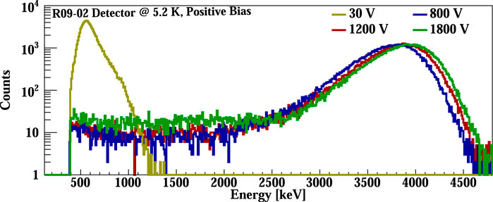
FIGURE 6. The energy deposition of 5.3 MeV α particles in an n-type detector operating in Method 1.
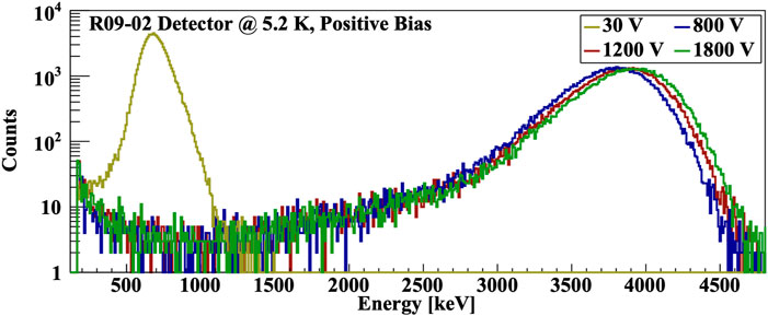
FIGURE 7. The energy deposition of 5.3 MeV α particles in an n-type detector operating in Method 2.
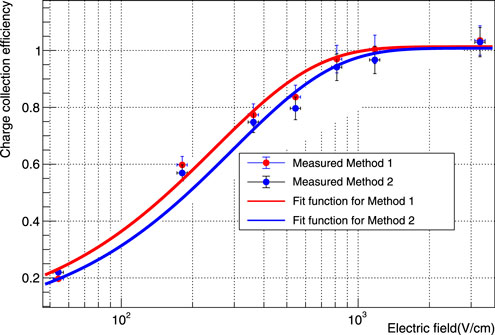
FIGURE 8. The graph of charge collection efficiency (ɛ) versus applied electric field (E) for Detector R09-02 at Method 1 and Method 2 has been plotted, with errors taken into account. The error in ɛ is based on the measurement of the mean energy deposition, while the error in E is largely influenced by the bias voltage applied. A fitting model,
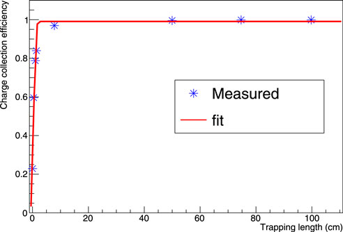
FIGURE 9. The graph of charge collection efficiency (ɛ) versus trapping length (λtrap) for an n-type Detector R09-02 has been plotted, taking into account the errors. The error in ɛ is derived from the measured mean energy deposition, while the error in λ is calculated using the propagation of error in Eq. 5. A fitting model,
The relationship between the trapping cross-section and the applied bias voltage obtained by using equation 6 is illustrated in Figure 10.
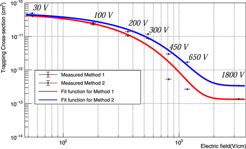
FIGURE 10. The graph of the variation of trapping Cross-Section (σtrap) with the applied bias field (E) in detector R09-02 has been plotted for both Method 1 and Method 2, considering the errors. The error in σtrap is calculated using the propagation of error in Eq. 6 while the error associated with E is primarily due to the applied bias voltage. A fitting model, σtrap = p0 − [(p1) ×exp(−p2 × E)], was used to fit the data, with the following fitted parameters for Method 1: p0 = (1.34 × 10⁻¹³ ± 1.83 × 10⁻¹⁴) cm2, p1 = −(5.17 × 10⁻¹¹ ± 7.4 × 10⁻¹²) cm2, and
The slope of the portion of the plot where the emission of charge carriers is dominant provides the charge-energy emission rate per unit of time (Et). By dividing Et by the binding energy of the dipole states or cluster dipole states (Eb), the emission rate of electrons en can be obtained. These emission rates are then utilized in equation 3 to numerically determine the binding energy for the respective dipole states or cluster dipole states. The calculated binding energies are presented in Table 1.
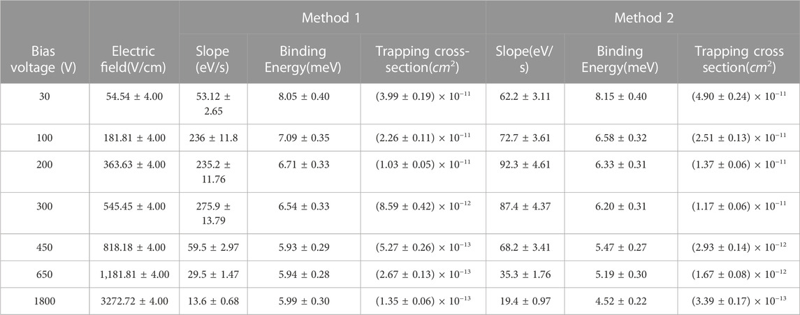
TABLE 1. The binding energy and trapping cross-section of R09-02 at 5.2 K for Method 1 and Method 2. The errors associated with each value are either the result of measurement errors or the error calculated from the equations used in the paper.
The binding energy measured by the detector in Method 1 pertains to the dipole states, whereas Method 2 provides data on the binding energy of the cluster dipole states. Additionally, the binding energy values obtained at varying bias voltages demonstrate a relationship with the electric field. As the electric field strength intensifies, the deformation potential undergoes modifications, particularly under higher electric fields. Consequently, the binding energy exhibits a dependency on the electric field’s magnitude, which should be appropriately described as the effective binding energy influenced by the electric field. Essentially, this implies that, in the presence of higher electric fields, carriers are more prone to escaping from traps, thereby enhancing their contribution to the overall charge transport within the detector. As shown in Figure 11, the binding energies are plotted as a function of the electric field at a temperature of 5.2 K.
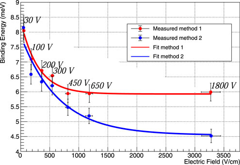
FIGURE 11. The binding energies of the dipole states and the cluster dipole states have been determined as a function of the applied electric field under two different operational methods, Method 1 and Method 2. The error in the binding energy measurement was calculated, while the error in the electric field measurement was dominated by the precision of the applied bias voltage. To analyze the data, a fit model was used, specifically EB =p0 + [(p1) × exp(−(p2) × E)], which resulted in the following fitted parameters: For Method 1, p0 was found to be (5.92±0.21) meV, p1 was (2.44 ± 0.52) meV, and p2 was (0.0033 ± 0.01)
In Method 1, the binding energies of the dipole states
4 Conclusion
Our study of binding energies and trapping cross-sections in an n-type Ge detector operating at a low temperature has revealed valuable insights. Our measurements indicate that the binding energy of dipole states is 8.369 ± 0.748 meV and the binding energy of cluster dipoles is 7.884 ± 0.644 meV, both of which are lower than the typical binding energy (around 10 meV) of ground state impurities in Ge. We found that at a temperature of 5.2 K, the thermal energy of 0.448 meV is much lower than these binding energies, indicating that the corresponding cluster dipole states and dipole states are thermally stable at a temperature of 5.2 K. The application of an electric field causes the smaller binding energy of cluster dipoles to result in increased de-trapping via impact ionization when compared to dipole states. The trapping cross section, which ranges from 3.99 × 10⁻¹¹cm2 to 1.35 × 10⁻¹³cm2, is primarily influenced by the electric field. Our findings further demonstrate that the binding energy and trapping cross-section decrease as the electric field within the detector increases. These low binding energies suggest the potential for developing a low-threshold detector using appropriately doped impurities in Ge for low-mass dark matter searches.
Data availability statement
The original contributions presented in the study are included in the article/supplementary material, further inquiries can be directed to the corresponding author.
Author contributions
SB: Investigation, Data curation, Formal Analysis, Methodology, Writing–original draft. DM: Investigation, Conceptualization, Funding acquisition, Resources, Supervision, Writing–review and editing. MR: Formal Analysis, Investigation, Methodology, Writing–review and editing. RP: Investigation, Resources, Writing–review and editing. KK: Investigation, Resources, Writing–review and editing. HM: Investigation, Resources, Writing–review and editing. GW: Investigation, Resources, Writing–review and editing.
Funding
The author(s) declare financial support was received for the research, authorship, and/or publication of this article. This work was supported in part by NSF OISE 1743790, DE-SC0004768, and a governor’s research center supported by the State of South Dakota.
Acknowledgments
The authors would like to thank Mark Amman for his instructions on fabricating planar detectors. We would also like to thank the Nuclear Science Division at Lawrence Berkeley National Laboratory for providing us with a testing cryostat.
Conflict of interest
The authors declare that the research was conducted in the absence of any commercial or financial relationships that could be construed as a potential conflict of interest.
The author DM declared that they were an editorial board member of Frontiers at the time of submission. This had no impact on the peer review process and the final decision.
Publisher’s note
All claims expressed in this article are solely those of the authors and do not necessarily represent those of their affiliated organizations, or those of the publisher, the editors and the reviewers. Any product that may be evaluated in this article, or claim that may be made by its manufacturer, is not guaranteed or endorsed by the publisher.
References
Aalbers, J., Akerib, D., Akerlof, C., Al Musalhi, A., Alder, F., Alqahtani, A., et al. (2022). First dark matter search results from the lux-zeplin (lz) experiment. arXiv preprint arXiv:2207.03764.
Agnese, R., Anderson, A. J., Asai, M., Balakishiyeva, D., Basu Thakur, R., Bauer, D., et al. (2014). Search for low-mass weakly interacting massive particles with supercdms. Phys. Rev. Lett. 112, 241302. doi:10.1103/physrevlett.112.241302
Agnese, R., Aralis, T., Aramaki, T., Arnquist, I., Azadbakht, E., Baker, W., et al. (2018). First dark matter constraints from a supercdms single-charge sensitive detector. Phys. Rev. Lett. 121, 051301. doi:10.1103/physrevlett.121.051301
Agnese, R., Aralis, T., Aramaki, T., Arnquist, I. J., Azadbakht, E., Baker, W., et al. (2019). Search for low-mass dark matter with cdmslite using a profile likelihood fit. Phys. Rev. D. 99, 062001. doi:10.1103/PhysRevD.99.062001
Ahmed, Z., Akerib, D., Arrenberg, S., Bailey, C., Balakishiyeva, D., Baudis, L., et al. (2011). Results from a low-energy analysis of the cdms ii germanium data. Phys. Rev. Lett. 106, 131302. doi:10.1103/physrevlett.106.131302
Al Kharusi, S., Anton, G., Badhrees, I., Barbeau, P., Beck, D., Belov, V., et al. (2023). Search for mev electron recoils from dark matter in exo-200. Phys. Rev. D. 107, 012007. doi:10.1103/physrevd.107.012007
Armengaud, E., Augier, C., Benoit, A., Bergé, L., Bergmann, T., Blümer, J., et al. (2012). Search for low-mass wimps with edelweiss-ii heat-and-ionization detectors. Phys. Rev. D. 86, 051701. doi:10.1103/physrevd.86.051701
Armengaud, E., Augier, C., Benoît, A., Bergé, L., Billard, J., Broniatowski, A., et al. (2018). Searches for electron interactions induced by new physics in the edelweiss-iii germanium bolometers. Phys. Rev. D. 98, 082004. doi:10.1103/physrevd.98.082004
Arnaud, Q., Armengaud, E., Augier, C., Benoît, A., Bergé, L., Billard, J., et al. (2020). First germanium-based constraints on sub-mev dark matter with the edelweiss experiment. Phys. Rev. Lett. 125, 141301. doi:10.1103/physrevlett.125.141301
Arnquist, I., Avignone, F., Barabash, A., Barton, C., Bertrand, F., Blalock, E., et al. (2022). α-event characterization and rejection in point-contact hpge detectors. Eur. Phys. J. C 82, 226. doi:10.1140/epjc/s10052-022-10161-y
Berghaus, K. V., Esposito, A., Essig, R., and Sholapurkar, M. (2023). The migdal effect in semiconductors for dark matter with masses below 100 mev. J. High Energy Phys. 2023, 23–31. doi:10.1007/jhep01(2023)023
Bhattarai, S., Mei, D.-M., and Raut, M.-S. (2021). Low-energy solar neutrino detection utilizing advanced germanium detectors. Journal of Physics G 50 (6), 065201.
Bhattarai, S., Panth, R., Wei, W., Mei, H., Mei, D., and Raut, M. (2020). Experimental study of electrical conduction mechanisms in p-type amorphous germanium (Ge) used as contacts for ge detectors in search for rare-event physics. The European Physics Journal C 80 (10). doi:10.1140/epjc/s10052-020-08529-z
Conwell, E. (1955). Hall effect and density of states in germanium. Phys. Rev. 99, 1195–1198. doi:10.1103/physrev.99.1195
Essig, R., Mardon, J., and Volansky, T. (2012). Direct detection of sub-gev dark matter. Phys. Rev. D. 85, 076007. doi:10.1103/physrevd.85.076007
He, Z. (2001). Review of the shockley–ramo theorem and its application in semiconductor gamma-ray detectors. Nucl. Instrum. Methods Phys. Res. Sect. A Accel. Spectrom. Detect. Assoc. Equip. 463, 250–267. doi:10.1016/s0168-9002(01)00223-6
Hochberg, Y., Zhao, Y., and Zurek, K. M. (2016). Superconducting detectors for superlight dark matter. Phys. Rev. Lett. 116, 011301. doi:10.1103/physrevlett.116.011301
IEEE (1993). “IEEE standard test procedures for high-purity germanium crystals for radiation detectors,” in Ieee std 1160-1993 (IEEE), 1–36. doi:10.1109/IEEESTD.1993.115139
Lee, E., James, R., Olsen, R., and Hermon, H. (1999). Compensation and trapping in cdznte radiation detectors studied by thermoelectric emission spectroscopy, thermally stimulated conductivity, and current-voltage measurements. J. Electron. Mater. 28, 766–773. doi:10.1007/s11664-999-0068-0
Mei, D.-M., Panth, R., Kooi, K., Mei, H., Bhattarai, S., Raut, M., et al. (2022). Evidence of cluster dipole states in germanium detectors operating at temperatures below 10 k. AIP Adv. 12, 065113. doi:10.1063/5.0094194
Mei, D.-M., Wang, G.-J., Mei, H., Yang, G., Liu, J., Wagner, M., et al. (2018). Direct detection of mev-scale dark matter utilizing germanium internal amplification for the charge created by the ionization of impurities. Eur. Phys. J. C 78, 187. doi:10.1140/epjc/s10052-018-5653-z
Mei, D., Mukund, R., Wei, W., Panth, R., Liu, J., Mei, H., et al. (2020). Impact of charge trapping on the energy resolution of ge detectors for rare-event physics searches. J. Phys. G Nucl. Part. Phys. 47, 105106. doi:10.1088/1361-6471/ab9796
Panth, R., Wei, W., Mei, D., Liu, J., Bhattarai, S., Mei, H., et al. (2022). Temperature-dependent charge barrier height of amorphous germanium contact detector. Nucl. Instrum. Methods Phys. Res. Sect. A Accel. Spectrom. Detect. Assoc. Equip. 1035, 166862. doi:10.1016/j.nima.2022.166862
Phipps, A. T. J. (2016). Ionization collection in detectors of the cryogenic dark matter search. Berkeley: University of California.
Raut, M.-S., Mei, H., Mei, D.-M., Bhattarai, S., Wei, W.-Z., Panth, R., et al. (2020). Characterization of high-purity germanium (ge) crystals for developing novel ge detectors. J. Instrum. 15, T10010. doi:10.1088/1748-0221/15/10/t10010
Sundqvist, K., Phipps, A., Bailey, C., Brink, P., Cabrera, B., Daal, M., et al. (2009). A measurement of electron and hole drift velocities in a germanium< 100> cdms detector, at a temperature of 31 millikelvin. AIP Conf. Proc. 1185, 128–131. doi:10.1063/1.3292299
Vénos, D., Geert, A. A. V., Severijns, N., Srnka, D., and Zákoucký, D. (2000). The behaviour of hpge detectors operating at temperatures below 77 k. Nucl. Instrum. Methods Phys. Res. Sect. A Accel. Spectrom. Detect. Assoc. Equip. 454, 403–408. doi:10.1016/s0168-9002(00)00494-0
Wang, G., Sun, Y., Yang, G., Xiang, W., Guan, Y., Mei, D., et al. (2012). Development of large size high-purity germanium crystal growth. J. Cryst. Growth 352, 27–30. doi:10.1016/j.jcrysgro.2012.01.018
Wei, W.-Z., and Mei, D.-M. (2017). Average energy expended per eh pair for germanium-based dark matter experiments. J. Instrum. 12, P04022. doi:10.1088/1748-0221/12/04/p04022
Wei, W.-Z., Meng, X.-H., Li, Y.-Y., Liu, J., Wang, G.-J., Mei, H., et al. (2018). Investigation of amorphous germanium contact properties with planar detectors made from usd-grown germanium crystals. J. Instrum. 13, P12026. doi:10.1088/1748-0221/13/12/p12026
Wei, W.-Z., Panth, R., Liu, J., Mei, H., Mei, D.-M., and Wang, G.-J. (2020). The impact of the charge barrier height on germanium (ge) detectors with amorphous-ge contacts for light dark matter searches. Eur. Phys. J. C 80, 472. doi:10.1140/epjc/s10052-020-8029-0
Yang, G., Govani, J., Mei, H., Guan, Y., Wang, G., Huang, M., et al. (2014). Investigation of influential factors on the purification of zone-refined germanium ingot. Cryst. Res. Technol. 49, 269–275. doi:10.1002/crat.201300418
Zhao, W., Yue, Q., Kang, K.-J., Cheng, J., Li, Y., Lin, S., et al. (2013). First results on low-mass wimps from the cdex-1 experiment at the China jinping underground laboratory. Phys. Rev. D. 88, 052004. doi:10.1103/physrevd.88.052004
Keywords: cryogenics, dipole states, cluster dipole states, trapping cross-section, binding energy
Citation: Bhattarai S, Mei D, Raut MS, Panth R, Kooi K, Mei H and Wang G (2023) Investigating binding energies and trapping cross-sections in an n-type Ge detector at low temperatures. Front. Detect. Sci. Technol 1:1275385. doi: 10.3389/fdest.2023.1275385
Received: 09 August 2023; Accepted: 06 October 2023;
Published: 26 October 2023.
Edited by:
Marco Cortesi, Michigan State University, United StatesReviewed by:
Luca Moleri, Weizmann Institute of Science, IsraelValerio Bocci, National Institute of Nuclear Physics of Rome Sapienza, Italy
Salvatore Di Carlo, Michigan State University, United States
Copyright © 2023 Bhattarai, Mei, Raut, Panth, Kooi, Mei and Wang. This is an open-access article distributed under the terms of the Creative Commons Attribution License (CC BY). The use, distribution or reproduction in other forums is permitted, provided the original author(s) and the copyright owner(s) are credited and that the original publication in this journal is cited, in accordance with accepted academic practice. No use, distribution or reproduction is permitted which does not comply with these terms.
*Correspondence: Dongming Mei, dongming.mei@usd.edu