Transmission Electron Microscopy Study on the Effect of Thermal and Electrical Stimuli on Ge2Te3 Based Memristor Devices
 Austin Shallcross1
  Krishnamurthy Mahalingam2,3 Eunsung Shin1
  Guru Subramanyam1*
  Md Shahanur Alam4 Tarek Taha4 Sabyasachi Ganguli2 Cynthia Bowers2,3 Benson Athey2,3 Albert Hilton2,3
  Ajit Roy2 Rohan Dhall5
- 1Center of Excellence for Thin-film Research and Surface Engineering (CETRASE), Department of Electrical and Computer Engineering, University of Dayton, Dayton, OH, United States
- 2Materials and Manufacturing Directorate, Air Force Research Laboratory, Dayton, OH, United States
- 3Universal Energy Systems, Dayton, OH, United States
- 4Parallel Cognitive Systems Lab, Department of Electrical and Computer Engineering, University of Dayton, Dayton, OH, United States
- 5National Center for Electron Microscopy, Molecular Foundry, Lawrence Berkeley National Laboratory, Berkeley, CA, United States
Memristor devices fabricated using the chalcogenide Ge2Te3 phase change thin films in a metal-insulator-metal structure are characterized using thermal and electrical stimuli in this study. Once the thermal and electrical stimuli are applied, cross-sectional transmission electron microscopy (TEM) and X-ray energy-dispersive spectroscopy (XEDS) analyses are performed to determine structural and compositional changes in the devices. Electrical measurements on these devices showed a need for increasing compliance current between cycles to initiate switching from low resistance state (LRS) to high resistance state (HRS). The measured resistance in HRS also exhibited a steady decrease with increase in the compliance current. High resolution TEM studies on devices in HRS showed the presence of residual crystalline phase at the top-electrode/dielectric interface, which may explain the observed dependence on compliance current. XEDS study revealed diffusion related processes at dielectric-electrode interface characterized, by the separation of Ge2Te3 into Ge- and Te- enriched interfacial layers. This was also accompanied by spikes in O level at these regions. Furthermore, in-situ heating experiments on as-grown thin films revealed a deleterious effect of Ti adhesive layer, wherein the in-diffusion of Ti leads to further degradation of the dielectric layer. This experimental physics-based study shows that the large HRS/LRS ratio below the current compliance limit of 1 mA and the ability to control the HRS and LRS by varying the compliance current are attractive for memristor and neuromorphic computing applications.
Introduction
Recently, various nanoscale memory devices have been demonstrated by the scientific community, which have the potential to store data in very high density and design new in-memory computing systems which mimic cognitive behavior for information processing, such as synaptic modifications, postsynaptic currents, and memory consolidation (Li et al., 2013). Memristor is one of the most studied devices for the new paradigm computing system. Leon Chua proposed the mathematical model of the memristor in 1971, which was claimed as the missing fourth fundamental element of the electrical circuits (Chua, 1971). The proposed memristive behavior was first realized after the nanoscale model (Yang et al., 2008) and experimental fabrication (Berzina et al., 2009). The signature characteristics of the presence of memresistance of a nanoscale device is the current-voltage relationship that shows a pinched hysteresis loop through the origin (Li et al., 2018). This property makes the device a suitable candidate for performing as a non-volatile memory device. The most vital characteristic of a memristor is that the conductance can be modified dynamically with input excitation. This dynamic behavior allows a memristor to be utilized as an artificial synapse which is a fundamental building block for hardware-based neuromorphic computing (Sokolov et al., 2021). In addition, memristors can be laid out in a high-density grid known as a crossbar structure (Taha et al., 2014), which gives them the potential to be fabricated with an areal density greater than that of synapses in the human brain (Burr et al., 2017). These crossbars can be used to produce high density, extremely low-power, neuromorphic hardware capable of performing many parallel operations in the analog domain (Chen et al., 2021).
Recent studies based on the simulation of memristor crossbars show promising results with these large high-density structures. Furthermore, it has been shown that neuromorphic systems based on memristor crossbars have potential to perform at a power efficiency of 6–8 orders of magnitude lower than that of traditional RISC processors (Taha et al., 2014). For ultra-high data storage and low power computing, many materials and devices have been investigated, such as resistive memory (Yang et al., 2008; Wang et al., 2017), ferroelectric materials (Chanthbouala et al., 2012), magnetic materials (Locatelli et al., 2014; Lequeux et al., 2016), and phase change materials (PCMs) (Xu et al., 2020).
PCMs attract more attention among the candidate materials due to their very high switching efficiency, stable data retention, long data endurance, and extraordinary scalability (Wuttig and Yamada, 2007; Zhao et al., 2007; Kuzum et al., 2012; Wang et al., 2019). In addition, their rapid phase transition, low energy consumption, stability at high temperature, and structural distinctiveness in the crystalline and amorphous states (Wuttig and Yamada, 2007) are attractive for fabricating phase-change random access memory (PCRAM) (Zhao et al., 2007) and electrical probe memory (Wang et al., 2019). The electrical properties of PCMs (e.g., resistivity/conductivity) can be controlled continuously by external stimulus, which opens application areas such as synaptic devices (memristor) and neuromorphic circuits (Kuzum et al., 2012).
For PCMs to change from amorphous to crystalline phase, they need to be heated to a temperature that allows crystallization. For phase transition from crystalline to amorphous phase, the temperature needs to be high enough to melt the material and then be rapidly cooled to freeze it in the amorphous/disorganized state. To affect the phase changes in the PCM based memristor, the PCM is sandwiched between bottom and top electrodes to create a metal/insulator/metal (MIM) structure. The MIM structure gives the ability to electrically bias the device and change its state through the flow of electrical current and the resulting Joule heating. To heat the structure to its melting point, a fast and a higher amplitude pulse is applied, quickly raising the temperature, followed by a rapid freeze causing the formation of the amorphous state / high resistance state (HRS). To change the device to its crystalline state / low resistance state (LRS), a voltage pulse with lower magnitude and longer width is applied which allows the device to be heated to a temperature that crystalizes the structure well below its melting point (El-Hinnawy et al., 2014; Le Gallo and Sebastian, 2020; Bruce et al., 2021; Singh et al., 2021; Eom et al., 2012). The large HRS/LRS ratio possibility in PCM based memristors is attractive for analog neuromorphic computing as one can obtain multiple resistance states corresponding to synapse weights.
In this study, we will focus on Ge2Te3 (GeTe), a chalcogenide PCM and investigate its phase change characteristics in a memristor structure through thermal and electrical stimuli. Once the thermal and electrical stimuli are applied, we compare results gathered from transmission electron microscopy (TEM) and X-ray energy-dispersive spectroscopy (XEDS) analyses to determine structural and compositional changes in the devices. The electrical measurements are corelated to the structural and compositional changes in the devices.
Experimental Methods
Fabrication
The GeTe-based memristor devices presented in this work were deposited in a Metal-Insulator-Metal (MIM) stack on Si wafers. The 5 × 5 µm devices were fabricated on a 100 nm thermal SiO2 coated high resistivity Si (100) wafer. Each device consists of a bottom metal electrode stack of Ti + Pt, a GeTe thin film layer, and a top metal electrode stack of Ti + Pt as shown in Figure 1. For patterning, the bottom and top electrodes, conventional photolithography, and lift-off processes were utilized as shown in Figure 1A. The top and bottom metal electrodes were deposited by e-beam evaporation technique. A 50 nm-thick GeTe thin film was grown as the memristive switching layer by pulsed laser deposition (PLD) technique on the bottom electrode stack. The GeTe film is sandwiched between the bottom and the top electrodes as shown in Figure 1B.
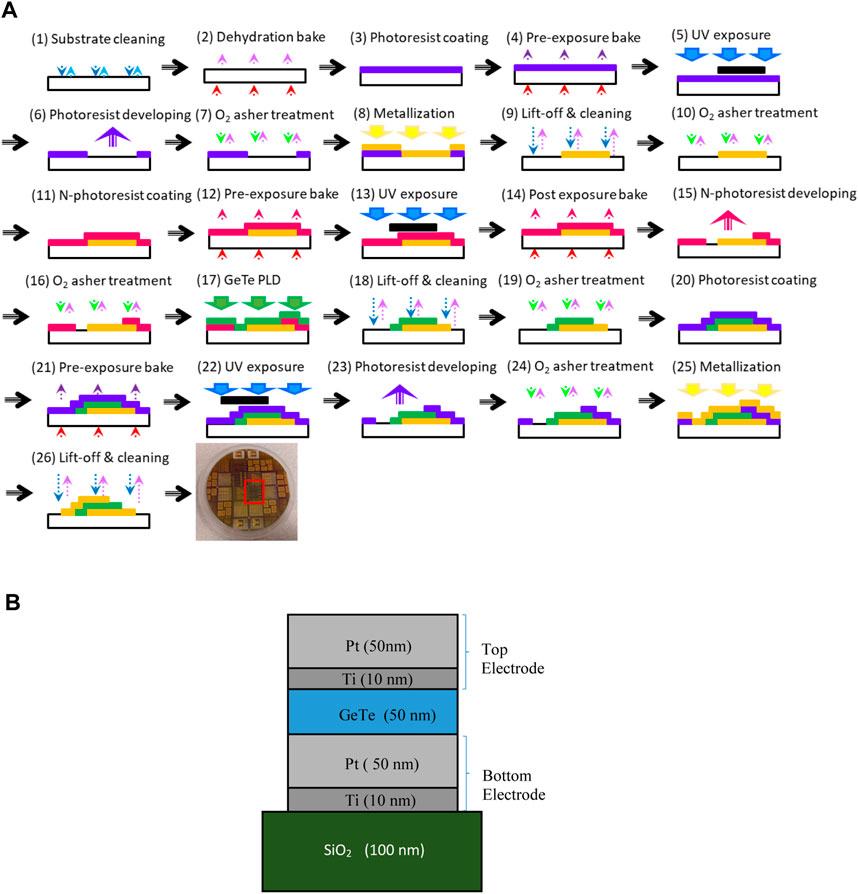
FIGURE 1. (A) Detailed steps in the device fabrication process and (B) the cross-section of the final device structure.
For fabricating the GeTe thin films, a homemade PLD system was utilized. The separation distance between the target and substrate was 50 mm, and the output of a KrF eximer laser (λ = 248 nm) was used to ablate a GeTe target. The laser energy density at the target surface was set to approximately 3.6 J/cm2, and the laser repetition rate was maintained at 10 Hz. During the deposition process, the PLD chamber pressure and the substrate temperature were maintained below 1 × 10⁻⁵ Torr and room temperature (< 25°C). For synthesizing 50 nm-thick film, 200 laser pulses were used.
Characterization
Samples for TEM observation were prepared by focused ion beam (FIB) milling using a Ga source. Before TEM observation, an additional cleaning procedure was performed by Ar-ion milling to reduce the surface amorphous layer and residual Ga that could be deposited due to the FIB process. The TEM observations were performed using a Talos 200-FX (ThermoFisher Scientific) TEM operated at an acceleration voltage of 200 kV. The samples were imaged using conventional high-resolution TEM (HRTEM) and high-angle annular dark-field scanning TEM (HAADF-STEM) techniques. In addition, X-ray energy dispersive spectroscopy (XEDS) measurements were performed in the HAADF-STEM mode, using the ChemiSTEMTM (ThermoFisher Scientific) technology. Acquisition and processing of the XEDS data was performed by spectrum imaging technique using the Esprit 1.9 (Brucker Inc.) software.
The electrical characterization measurements were carried out using a MicroXact probe station and Keysight B1500A semiconductor analyzer with two waveform generators/fast measurement units (WGFMU) modules. The set (crystallization) and reset (amorphization) processes of the GeTe memristors were preformed utilizing electrical pulses. The set pulse has an amplitude of 2.5 V, with a pulse-width of 15 µs, a rise time of 1 ns and a fall time of 5 µs. The reset pulse has an amplitude in the range of 4 – 10 V with a pulse-width of 1 µs and a rise and fall time of 1 ns. Since devices are switched between the high and low resistance states, a read operation is performed using a low voltage DC sweep from 0–100 mV to determine the change of resistance between the HRS and LRS. Due to the lower voltage compared to the set and reset process, the GeTe layer does not undergo any phase changes during the read operation and will maintain that resistance until another pulse with sufficient potential is applied to the device. Devices were also cycled using a DC voltage sweep from −2 V– + 4 V – -2 V with various current compliance (CC) limits.
Results and Discussions
Electrical Measurements
Devices were first tested for proper switching through the set and reset pulses. By applying repetitive set pulses, the devices were locally heated to > 250°C causing crystallization to occur. After setting the devices to the LRS, the device resistance was between 1.5 and 20 kΩ. A single reset pulse is applied to reset the device in the HRS. Once reset, the resistance would typically read approximately 500 kΩ or show open circuit indicating that the analyzer could not measure any current through the device.
Additionally, with the information gathered from the TEM analysis on the heated device showing a significant change in its structure, devices were then tested under strenuous electrical stimuli to determine if similar structural changes are observed for electrical tests. Devices were first cycled with a 500 µA current compliance (CC) limit which was then increased to 1, 1.5, 2, and 5 mA. After multiple cycles at the 500 µA CC limit, the hysteresis loop began to pinch (Figures 2A,B), showing little to no changes in resistance. After five DC sweeps the device showed a completely pinched hysteresis. When increasing the CC, no pattern was observed in the number of cycles required to see the pinched hysteresis loop. It was determined that the negative voltage during the DC sweep drove the device’s resistance further into the LRS, causing the pinching of the hysteresis. This pinching represents a unipolar switching behavior for the devices due to the phase change characteristic of GeTe. Once a completed pinched hysteresis was observed at the 500 µA CC limit, the device’s LRS was read at approximately 5 kΩ. To switch the device into its HRS after cycling, the 1 µs and 4 V reset pulse was applied. After resetting, the device’s resistance showed an increase to approximately 100 kΩ. Due to the device not reaching its previous HRS values of approximately 500 kΩ, the pulse amplitude was increased to 6 and 8 V but no further change in resistance was observed.

FIGURE 2. Plot of the I-V characteristic GeTe memristor showing switching behavior in the form of a hysteresis loop (A) and pinched hysteresis (B,C) DC voltage sweep at 500 µA current compliance after cycling at 1 mA (red) and a DC voltage sweep at 1 mA after the 500 µA sweep (black).
The previous process was then repeated with an increased CC limit of 1 mA. The results showed similar properties when compared to the 500 µA tests. The LRS resistance after cycling was 2 kΩ, which indicates that the higher CC limit also causes a lower resistance. After resetting, the highest obtainable resistance was now 25 kΩ compared to the previous 100 kΩ. The device was then retested at a 500 µA CC limit to determine if it will maintain similar I-V characteristics to the previous 500 µA cycles. It was observed that the device was already near a completely pinched hysteresis loop. Without resetting, the CC limit is raised back to 1 mA and a more evident change in resistance is observed (Figure 2C). This indicates that the device is no longer operational at CC limits less than 1 mA. Furthermore, after the 1.5, 2 and 5 mA CC limit testing the same trend is observed. As illustrated in Figure 3A, the LRS resistance values continue to decrease to approximately 1.5 kΩ, 1 kΩ, and 850 Ω. Concurrently, the HRS resistance values drop to approximately 10 kΩ, 8 kΩ, and 5 kΩ. With the continued decrease in the HRS’s highest achievable resistance under increasing current compliance indicates that an irreversible process is taking place within the device.
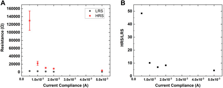
FIGURE 3. (A) Low resistance state values following DC sweeps at current compliances of 500 µA, 1 mA, 1.5 mA, 2 and 5 mA (black) and high resistance state values following each reset pulse (red) for a single device (B) HRS/LRS ratio for each current compliance.
In spite of the dropping HRS and LRS levels, the ratio of the HRS/LRS stays close to 10 up to a CC of 2 mA and drops down to roughly 5 at a CC of 5 mA as shown in Figure 3B. HRS/LRS ratio above 10 is possible if we operate below the CC of 1 mA. This region below CC of 1 mA could be useful for low power neuromorphic computing. Clearly, the HRS values and the HRS/LRS ratio are tunable by varying the current compliance. This could be useful for implementing artificial synapses in neuromorphic processors.
Transmission Electron Microscopy Analysis
TEM investigations were performed on the PCM based memristor devices to understand the HRS dependence on current compliance presented in Figure 3. While the switching between the two resistance states is primarily driven by amorphous to crystalline transition due to electrical bias induced Joule heating, it is important to note that the atomistic processes at the dielectric/electrode interface may also play a role in the observed dependence. Based on these considerations, the TEM analysis was focused on two aspects: HAADF-STEM/XEDS studies to examine compositional changes due to inter-diffusion at the dielectric/electrode interfaces and HRTEM imaging to examine structural changes in the overall device region. Furthermore, these investigations were performed on samples extracted from actual devices and compared with in-situ heating experiments performed on GeTe thin films in the as-grown condition (prior to device fabrication).
Figure 4 shows the XEDS map (a) and the corresponding line profiles of elemental distribution (b) across the device structure. These results were obtained from the device tested in Figure 3 with a final compliance current of 5 mA. An examination of Ge and Te profiles (Figure 4B) reveals separated spikes adjacent to the top electrode region, indicating dissociation of Ge2Te3 into Ge- and Te- enriched regions. In addition, the formation of enriched regions is accompanied.
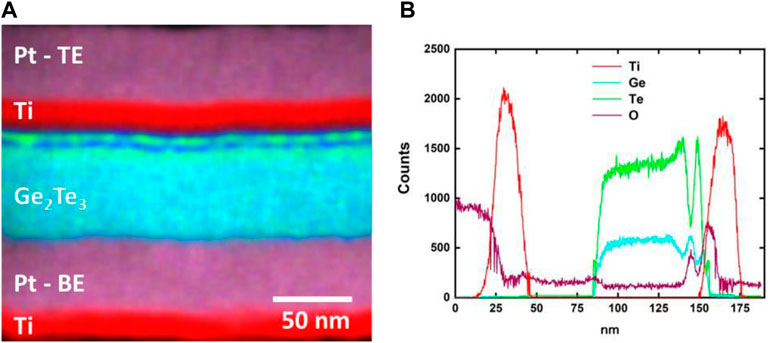
FIGURE 4. (A) XEDS map and (B) elemental line profiles of overall device structure after electrical biasing. Note that the top and bottom Pt electrodes are abbreviated TE and BE, respectively.
by spikes in the O profile. The dissociation of Ge2Te3 appears as alternating green and blue bands adjacent to the top Pt electrode in XEDS map (Figure 4A). Although not shown, similar results were also observed in the XEDS data obtained from devices in the unbiased condition, indicating that Ge2Te3 is triggered by surface oxidation during device processing.
Further studies were performed by HRTEM to examine the structure of Ge and Te enriched interfacial layers observed in the XEDS maps. The HRTEM images of the top electrode region extracted from devices before and after electrical biasing are shown in Figure 5 (a) and (b), respectively. The region corresponding to the spike in O profile is identified in the two images. Furthermore, the regions corresponding to the Ge- and Te- enrichment in the XEDS map are revealed by subtle change in contrast in the Ge2Te3 region adjacent to the oxide layer. An examination of the region beneath the oxide layer in the unbiased sample (Figure 5A) shows the expected amorphous structure. However, an examination of a similar region in the electrically biased sample (Figure 5B) clearly shows the presence of a crystalline phase, indicating phase change due to Joule heating.
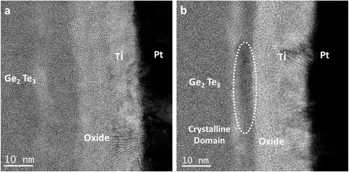
FIGURE 5. HRTEM image of top dielectric/electrode interface showing (A) an amorphous structure in Ge2Te3 prior to electrical biasing and (B) the presence of a crystalline domain in dielectric/ electrode interface after cyclic electrical biasing to HRS (enclosed in the dotted region).
To further understand the results from the XEDS and HRTEM described above, an in-situ heating experiment was performed on device structures in the as-grown condition, with the temperature gradually raised in steps of 20°C up to 450°C. HAADF-STEM imaging and XEDS measurements were performed at different step intervals, after allowing settling time for sample thermal drift. Figure 6 shows the HAADF-TEM images of device structure in the as-grown condition (Figure 6A) and after heating to 200°C (Figure 6B), wherein the individual layers are identified. Significant changes in contrast are evident at the interfacial regions adjoining the Ge2Te3 layer and the top/bottom electrodes. In particular, we observe the appearance of additional layers in the vicinity of the Ti adhesive layer at the top electrode interface. Furthermore, HRTEM image of the Ge2Te3 layer (Figure 6C) after heating to 200°C indicated crystalline phase formation (it is noted that the HRTEM image of Ge2Te3 layer at room temperature showed amorphous structure as in Figure 5A). The formation of crystalline phase could explain the lowering in resistance observed in Figure 3. Furthermore, its persistence could also explain the need for higher compliance current to initiate switching.
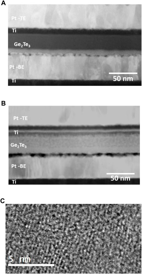
FIGURE 6. HAADF-STEM images showing the overall device structure in (A) as-grown condition at room temperature, (B) after heating to 200°C and (C) HRTEM image of Ge2Te3 after heating to 200°C.
To understand the origin of the observed change in contrast at the top electrode in the HAADF-STEM images, we compared the XEDS maps acquired at room temperature (Figure 7A) and at 200°C (Figure 7B). A comparison of the two maps reveal significant intermixing upon heating at the top Ti/Ge2Te3 interface as indicated by the presence of a distinct green band corresponding to this region in Figure 7B. Further insight on the nature of this intermixing is gained by examination of the line profile of the individual elemental distribution across layers in the device structure shown in Figure 8. The aforementioned spikes in the Ge and Te distribution are present in the as-grown condition at room temperature (Figure 8A), although to a lesser degree in comparison to those observed in Figure 4, presumably due to lower O level observed in the line profile. However, upon heating to 200°C significant increase of Ge- and Te- spikes is evident, which is also accompanied by noticeable increase in the O-profile. Furthermore, a comparison of Ti profile shows noticeable change in Ti at the top electrode after heating, as indicated by a shrinking in profile closer to the electrode and the presence of a shoulder in the region corresponding to the spike in the Te profile. In comparison, the Ti profile at the bottom electrode does not exhibit noticeable change upon heating. The XEDS profiles indicate significant in diffusion of Ti, which upon further heating results in the eventual dissolution of Ti into the Ge2Te3 layer as shown in the XEDS maps in Figure 9.
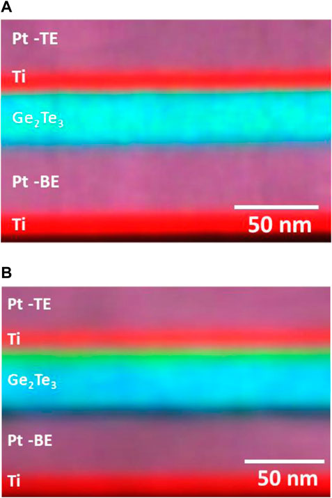
FIGURE 7. XEDS maps of the device structure (A) in the as-grown condition at room temperature and (B) after heating to 200°C.
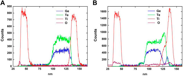
FIGURE 8. Elemental Line profiles from the XEDS maps of the device structure (A) in the preformed condition and (B) after heating to 200°C.
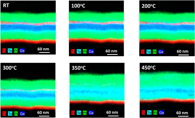
FIGURE 9. Composite XEDS elemental maps obtained from in-situ heating experiments starting at room temperature (RT), showing in-diffusion of Ti into the Ge2Te3 layer with increase in temperature.
The role of O observed in the in-situ TEM heating experiments are consistent with the results reported in the literature, wherein the Ge2Te3 separation is caused by an oxidation process triggered by preferential migration of Ge towards the surface (Berthier et al., 2017; Pierre et al., 2016). In addition, the oxidation could also result in a lowering of the crystallization temperature and resistivity which supports the observations made in the HRTEM imaging and electrical biasing experiments. In this study, the oxidation process seems to be enhanced much more during the device fabrication process due to the break in vacuum after the deposition of the electrodes. It is also worth noting that the observations pertaining to Ti diffusion are also consistent with earlier annealing studies reported on bulk samples (Loubriat et al., 2011), indicating that the effect of TEM sample preparation is not significant in the present study. Although the XEDS profiles may seem to indicate that the Ti diffusion in the electrically biased samples is not as drastic as those seen in the in-situ heating experiments, it should be noted that the heating experiments were performed over several minutes, whereas bias experiments are conducted over shorter pulses. The deleterious effect of Ti diffusion is still likely to be relevant for reliable device operation in the long-term. These observations indicate the need for developing mature processing steps to combat the effects of O and Ti in Ge2Te3-based memristor devices.
Conclusion
Memristor devices fabricated using the chalcogenide Ge2Te3 phase change thin films in a metal-insulator-metal structure are characterized using thermal and electrical stimuli in this experimental study. A cross-sectional transmission electron microscopy (TEM) study is performed to investigate microstructural phenomena that control the switching behavior and integrity of the dielectric-electrode interface in Ge2Te3-based memristor devices. We report successful switching of the GeTe memristors with distinct high and low resistance states. Electrical measurements on these devices showed steady decrease in resistance at HRS and a higher compliance current required to initiate LRS to HRS switching. Cross-sectional TEM studies indicate that this dependence could be explained by crystalline phase formation at around 200°C. However, the separation of the GeTe layer with the spike in oxygen upon heating and diffusion of Ti adhesive layer could have a significant influence on the switching characteristics. This experimental study shows that the ability to control the HRS and LRS by varying the compliance current are attractive for implementing artificial synapse in neuromorphic computing applications.
Data Availability Statement
The original contributions presented in the study are included in the article/Supplementary Material, further inquiries can be directed to the corresponding author.
Author Contributions
AS and KM are to be treated as first authors for the manuscript based on their contributions. All other authors contributed equally to the manuscript.
Funding
Work at the Molecular Foundry was supported by the Office of Science, Office of Basic Energy Sciences, of the U.S. Department of Energy under contract no. DE-AC02-05CH11231. The work at the University of Dayton was partially supported by the National Science Foundation under award no. 1718633, and Strategic Ohio Council for Higher Education (SOCHE).
Conflict of Interest
Authors KM, CB, BA and AH were employed by the company Universal Energy Systems.
The remaining authors declare that the research was conducted in the absence of any commercial or financial relationships that could be construed as a potential conflict of interest.
Publisher’s Note
All claims expressed in this article are solely those of the authors and do not necessarily represent those of their affiliated organizations, or those of the publisher, the editors and the reviewers. Any product that may be evaluated in this article, or claim that may be made by its manufacturer, is not guaranteed or endorsed by the publisher.
References
Berthier, R., Bernier, N., Cooper, D., Sabbione, C., Hippert, F., and Noé, P. (2017). In Situ observation of the Impact of Surface Oxidation on the Crystallization Mechanism of GeTe Phase-Change Thin Films by Scanning Transmission Electron Microscopy. J. Appl. Phys. 122, 115304. doi:10.1063/1.5002637
Berzina, T., Smerieri, A., Bernabò, M., Pucci, A., Ruggeri, G., Erokhin, V., et al. (2009). Optimization of an Organic Memristor as an Adaptive Memory Element. J. Appl. Phys. 105 (12), 124515. doi:10.1063/1.3153944
Bruce, R. L., Sarwat, S. G., Boybat, I., Cheng, C.-W., Kim, W., Nandakumar, S. R., et al. (2021). “Mushroom-Type Phase Change Memory with Projection Liner: An Array-Level Demonstration of Conductance Drift and Noise Mitigation,” in 2021 IEEE International Reliability Physics Symposium (IRPS), Monterey, CA, March 21–25, 2021. doi:10.1109/IRPS46558.2021.9405191
Burr, G. W., Shelby, R. M., Sebastian, A., Kim, S., Kim, S., Sidler, S., et al. (2017). Neuromorphic Computing Using Non-volatile Memory. Adv. Phys. X 2 (1), 89–124. doi:10.1080/23746149.2016.1259585
Chanthbouala, A., Garcia, V., Cherifi, R. O., Bouzehouane, K., Fusil, S., Moya, X., et al. (2012). A Ferroelectric Memristor. Nat. Mater. 11 (10), 860–864. doi:10.1038/nmat3415
Chen, J., Li, J., Li, Y., and Miao, X. (2021). Multiply Accumulate Operations in Memristor Crossbar Arrays for Analog Computing. J. Semicond. 42 (1), 013104. doi:10.1088/1674-4926/42/1/013104
Chua, L. (1971). Memristor-the Missing Circuit Element. IEEE Trans. Circuit Theor. 18 (5), 507–519. doi:10.1109/tct.1971.1083337
El-Hinnawy, N., Borodulin, P., Wagner, B. P., King, M. R., Jones, E. B., Howell, R. S., et al. (2014). Low-loss Latching Microwave Switch Using Thermally Pulsed Non-volatile Chalcogenide Phase Change Materials. Appl. Phys. Lett. 105, 013501. doi:10.1063/1.4885388
Eom, T., Choi, S., Choi, B. J., Lee, M. H., Gwon, T., Rha, S. H., et al. (2012). Conformal Formation of (GeTe2)(1-x)(Sb2Te3)x Layers by Atomic Layer Deposition for Nanoscale Phase Change Memories. Chem. Mater. 24 (11), 2099–2110. doi:10.1021/cm300539a
Kuzum, D., Jeyasingh, R. G. D., Lee, B., and Wong, H.-S. P. (2012). Nanoelectronic Programmable Synapses Based on Phase Change Materials for Brain-Inspired Computing. Nano Lett. 12 (5), 2179–2186. doi:10.1021/nl201040y
Le Gallo, M., and Sebastian, A. (2020). An Overview of Phase-Change Memory Device Physics. J. Phys. D: Appl. Phys. 53, 213002. doi:10.1088/1361-6463/ab7794
Lequeux, S., Sampaio, J., Cros, V., Yakushiji, K., Fukushima, A., Matsumoto, R., et al. (2016). A Magnetic Synapse: Multilevel Spin-Torque Memristor with Perpendicular Anisotropy. Sci. Rep. 6 (1), 31510–31517. doi:10.1038/srep31510
Li, Y., Zhong, Y., Xu, L., Zhang, J., Xu, X., Sun, H., et al. (2013). Ultrafast Synaptic Events in a Chalcogenide Memristor. Sci. Rep. 3 (1), 1619–1627. doi:10.1038/srep01619
Li, Y., Wang, Z., Midya, R., Xia, Q., and Yang, J. J. (2018). Review of Memristor Devices in Neuromorphic Computing: Materials Sciences and Device Challenges. J. Phys. D: Appl. Phys. 51 (50), 503002. doi:10.1088/1361-6463/aade3f
Locatelli, N., Cros, V., and Grollier, J. (2014). Spin-torque Building Blocks. Nat. Mater 13 (1), 11–20. doi:10.1038/nmat3823
Loubriat, S., Muyard, D., Fillot, F., Roule, A., Veillerot, M., Barnes, J. P., et al. (2011). GeTe Phase Change Material and Ti Based Electrode: Study of thermal Stability and Adhesion. Microelectron. Eng. 88, 817–821. doi:10.1016/j.mee.2010.07.032
Pierre, N., Sabbione, C., Bernier, N., Castellani, N., Fillot, F., and Hippert, F. (2016). Impact of Interfaces on Scenario of Crystallization of Phase Change Materials. Acta Mater. 110, 142–148. doi:10.1016/j.actamat.2016.03.022
Singh, K., Kumari, S., Singh, H., Bala, N., Singh, P., Kumar, A., et al. (2021). A Review on GeTe Thin Film-Based Phase-Change Materials. Appl. Nanosci. 11, 0123456789. doi:10.1007/s13204-021-01911-7
Sokolov, A. S., Abbas, H., Abbas, Y., and Choi, C. (2021). Towards Engineering in Memristors for Emerging Memory and Neuromorphic Computing: A Review. J. Semicond. 42 (1), 013101. doi:10.1088/1674-4926/42/1/013101
Taha, T. M., Hasan, R., and Yakopcic, C. (2014). “Memristor Crossbar Based Multicore Neuromorphic Processors,” in 2014 27th IEEE International System-on-Chip Conference (SOCC), Las Vegas, NV, September 2–5, 2014, 383–389. doi:10.1109/socc.2014.6948959
Wang, Z., Joshi, S., Savel’ev, S. E., Jiang, H., Midya, R., Lin, P., et al. (2017). Memristors with Diffusive Dynamics as Synaptic Emulators for Neuromorphic Computing. Nat. Mater. 16 (1), 101–108. doi:10.1038/nmat4756
Wang, L., Yang, C.-H., Wen, J., and Xiong, B.-S. (2019). Reading Contrast of Phase-Change Electrical Probe Memory in Multiple Bit Array. IEEE Trans. Nanotechnol. 18, 260–269. doi:10.1109/tnano.2019.2901779
Wuttig, M., and Yamada, N. (2007). Phase-change Materials for Rewriteable Data Storage. Nat. Mater. 6 (11), 824–832. doi:10.1038/nmat2009
Xu, M., Mai, X., Lin, J., Zhang, W., Li, Y., He, Y., et al. (2020). Recent Advances on Neuromorphic Devices Based on Chalcogenide Phase‐Change Materials. Adv. Funct. Mater. 30 (50), 2003419. doi:10.1002/adfm.202003419
Yang, J. J., Pickett, M. D., Li, X., Ohlberg, D. A. A., Stewart, D. R., and Williams, R. S. (2008). Memristive Switching Mechanism for Metal/oxide/metal Nanodevices. Nat. Nanotech. 3 (7), 429–433. doi:10.1038/nnano.2008.160
Keywords: memristor, chalcogenide, phase change materials, resistive switching, resistive memory, TEM
Citation: Shallcross A, Mahalingam K, Shin E, Subramanyam G, Alam MS, Taha T, Ganguli S, Bowers C, Athey B, Hilton A, Roy A and Dhall R (2022) Transmission Electron Microscopy Study on the Effect of Thermal and Electrical Stimuli on Ge2Te3 Based Memristor Devices. Front. Electron. 3:872163. doi: 10.3389/felec.2022.872163
Received: 09 February 2022; Accepted: 23 March 2022;
Published: 26 April 2022.
Edited by:
Amirali Amirsoleimani, York University, CanadaReviewed by:
Yao-Feng Chang, Intel, United StatesFei Hui, Technion Israel Institute of Technology, Israel
Copyright © 2022 Shallcross, Mahalingam, Shin, Subramanyam, Alam, Taha, Ganguli, Bowers, Athey, Hilton, Roy and Dhall. This is an open-access article distributed under the terms of the Creative Commons Attribution License (CC BY). The use, distribution or reproduction in other forums is permitted, provided the original author(s) and the copyright owner(s) are credited and that the original publication in this journal is cited, in accordance with accepted academic practice. No use, distribution or reproduction is permitted which does not comply with these terms.
*Correspondence: Guru Subramanyam, gsubramanyam1@udayton.edu