Hardware acceleration of DNA pattern matching using analog resistive CAMs
 Jinane Bazzi
 Jana Sweidan1
  Mohammed E. Fouda
 Ahmed M. Eltawil
- 1King Abdullah University of Science and Technology, Thuwal, Saudi Arabia
- 2Rain Neuromorphics Inc., San Francisco, CA, United States
- 3ECE Department, American University of Beirut, Beirut, Lebanon
- 4Synopsys Inc., Austin, TX, United States
DNA pattern matching is essential for many widely used bioinformatics applications. Disease diagnosis is one of these applications since analyzing changes in DNA sequences can increase our understanding of possible genetic diseases. The remarkable growth in the size of DNA datasets has resulted in challenges in discovering DNA patterns efficiently in terms of run time and power consumption. In this paper, we propose an efficient pipelined hardware accelerator that determines the chance of the occurrence of repeat-expansion diseases using DNA pattern matching. The proposed design parallelizes the DNA pattern matching task using associative memory realized with analog content-addressable memory and implements an algorithm that returns the maximum number of consecutive occurrences of a specific pattern within a DNA sequence. We fully implement all the required hardware circuits with PTM 45-nm technology, and we evaluate the proposed architecture on a practical human DNA dataset. The results show that our design is energy-efficient and accelerates the DNA pattern matching task by more than 100× compared to the approaches described in the literature.
1 Introduction
Deoxyribonucleic acid (DNA) pattern matching is the workhorse for several bioinformatics applications. Disease diagnosis is the most popular among them (Mane and Pangu, 2016). Scientists rely heavily on DNA pattern matching to explore and detect possible diseases that can arise due to changes in DNA sequences.
A DNA molecule contains the information needed for the development and functioning of organisms. DNA has four basic nucleotide characters: adenine (A), cytosine (C), guanine (G), and thymine (T). A combination of these characters forms a DNA sequence that is unique to each organism. Genes are subsequences of DNA that carry information about an organism’s physical traits. It is important to understand and analyze gene sequences since changes in these sequences, referred to as mutations, may have harmful effects on the organism in which they occur, for example, by causing a genetic disorder. One of the major changes is nucleotide repeats, in which a specific DNA pattern repeat is expanded abnormally within a region of DNA. More than 40 repeat-expansion diseases are known, most of which primarily affect the nervous system. Expanded trinucleotide-repeat disorders, which are caused by the unstable expansion of three nucleotides consecutively repeated, were the first to be discovered, and they remain the most frequent. Recently, the list of repeat-expansion diseases has increased to include tetra-, penta-, hexa-, and even dodeca-nucleotide repeat expansions (Paulson, 2018). Table 1 shows some examples of diseases and their corresponding genes and pattern counts. DNA pattern matching can be used to detect these diseases by identifying the number of consecutive occurrences of the corresponding pattern.
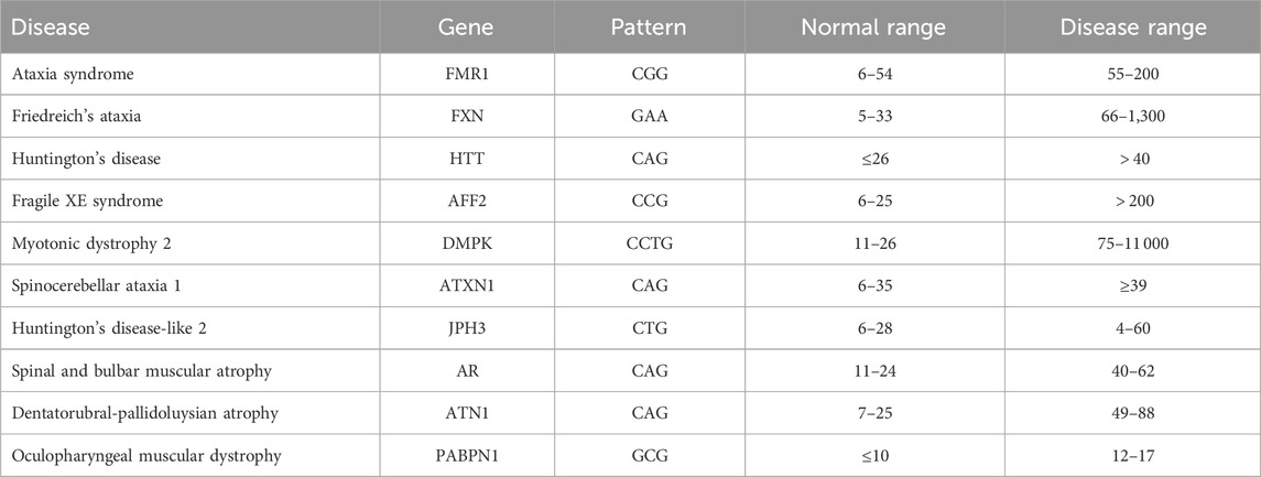
TABLE 1. Examples of nucleotide-repeat disorders. Based on data from (Usdin, 2008; Lalonde et al., 2020).
Datasets of DNA sequences require a huge amount of storage. For instance, the human genome has around 3.1647 billion DNA base pairs (Adjeroh et al., 2002). This significant volume of DNA data imposes a challenge in performing DNA pattern matching efficiently. Accordingly, many works have been proposed in the literature to accelerate DNA pattern matching, such as acceleration systems using parallel computing platforms, for instance, GPUs (Adey, 2013). To accelerate search operations with large DNA sequences, in (Raju et al., 2018), the authors proposed three DNA pattern matching algorithms running on CPU: Linear Array, Butterfly, and Divide and Conquer algorithms. Although these algorithms showed an improvement in terms of time cost compared to existing algorithms (Brute Force (Cormen et al., 2022), KMP (Knuth et al., 1977), and Boyer–Moore (Boyer and Moore, 1977)), they remain computationally intensive and need to be further accelerated by hardware. Therefore, various works have explored the utilization of hardware accelerators to implement DNA pattern matching aiming to further reduce its execution time. For instance, in (Lei et al., 2016), the authors proposed SCADIS, an FPGA-based short read mapping accelerator utilizing the KMP algorithm. Implemented on a Xilinx Zynq development board, SCADIS achieved a 2× speedup compared to an ARM Cortex-A9 processor with acceptable cost and higher energy efficiency. Kim et al., 2020 introduced GenieHD, a novel pattern matching algorithm employing hyperdimensional computing. GenieHD outperformed the approach in (Lei et al., 2016), implemented on the same board.
Pattern matching can be categorized into various types (Mahmud et al., 2023). In terms of accuracy, the two primary types are exact and approximate pattern matching (Hakak et al., 2019; Markić et al., 2020). In approximate pattern matching (Kaplan et al., 2018; Kim et al., 2018; Laguna et al., 2020; Khatamifard et al., 2021), the goal is to identify patterns that are similar rather than identical. This means that mismatching characters may exist between the query pattern and the stored data entry. Consequently, a certain level of error is acceptable, and such a stored pattern should still be considered a match. This is important for cases with DNA sequencing errors. In contrast, our focus in this paper is on the exact pattern matching problem, which involves identifying all precise occurrences of a pattern in a DNA sequence. Our objective is to develop a domain-specific hardware accelerator to accelerate the exact DNA pattern matching task, as opposed to relying on general-purpose designs that are slower and more energy-consuming.
Associative memory (AM) is a powerful tool for in-memory computing. It is a form of storage device that can be searched in a parallel manner (Arsovski et al., 2003). The address of any content that matches an input data word is returned. The fast parallel search offered by AM means that this type of memory is used in a variety of applications with big data workloads, for instance, genomic analysis, for which the amount of data has experienced exponential growth in recent years (Garzón et al., 2022). Content-addressable memory (CAMs) is one way to implement AMs. CAMs can be realized with different technologies, for instance, digital CAMs are implemented using standard CMOS and flip-flops (Kokosiński and Sikora, 2002). However, these types of architecture have high power consumption and low density. Accordingly, various emerging resistive device technologies have been used to implement some recently proposed CAMs, benefiting from their non-volatility and high packing density (Fouda et al., 2022). Examples of resistive devices include ReRAM, phase change memory, magnetic tunneling junctions, and ferroelectric devices (Yin et al., 2020). Resistive-based CAMs have an order of magnitude improvement in power consumption and area. Moreover, they can store wide intervals, thereby enabling continuous search ranges for analog applications. In this work, we study memristor-based analog CAM (aCAM), which has a higher memory density and lower power intake. aCAM could accelerate existing applications and may enable potential new uses (Li et al., 2020).
In this paper, we propose a hardware architecture that can perform DNA pattern matching efficiently with low cost in terms of latency and power consumption. The proposed hardware accelerator uses ReRAM-based AM and implements a hardware-friendly algorithm, in which input words are compared to the entire pattern simultaneously using AM. Our objective is to detect the presence of possible repeat-expansion diseases. The contributions of this paper are summarized in the following points:
• We propose a hardware-friendly pipelined algorithm for DNA pattern matching.
• We propose the full architecture for a parallel-processing hardware accelerator. It uses AM to enable fast parallel searches and matching. We design all the circuits needed to implement the proposed algorithm.
• We evaluate the performance of the proposed design in terms of overall energy and latency by testing it on human DNA sequences to detect the presence of possible trinucleotide repeat-expansion diseases. The results show the remarkable energy efficiency of our design, along with a significant improvement in the speed of the DNA pattern matching task, outperforming existing works in the literature by more than 100×.
The remainder of the paper is organized as follows. Section 2 discusses DNA pattern matching and our proposed hardware-friendly matching algorithm. Section 3 describes the proposed hardware architecture and its implementation. Section 4 presents the experimental setup. Section 5 reports the evaluation results in terms of latency, energy, and area. Finally, Section 6 concludes the work.
2 DNA pattern search
Pattern matching is the process of finding all occurrences of a pattern in a text. In DNA pattern matching, a DNA sequence is scanned to detect the instances of a pattern of nucleotides within it.
2.1 Proposed hardware-friendly matching algorithm
In our work, we propose a hardware accelerator that uses AM to analyze DNA data more efficiently in parallel. We propose a hardware-friendly algorithm to be implemented by the accelerator design. Our algorithm returns the maximum number of consecutive pattern repeats instead of the total number of occurrences, because our objective is to detect possible repeat-expansion diseases where a specific pattern is abnormally expanded.
Figure 1 illustrates the proposed high-level design, which consists of an associative memory (AM), binary memory, and a pattern detector. The DNA data is stored in an M × N AM array. Since AM allows parallel searches, p cells are activated in each row during each cycle, enabling the simultaneous parallel comparison of a pattern of length p to these activated cells across all M rows. To track pattern occurrences, a binary memory is used. This memory stores ‘1’ at locations corresponding to the indices of pattern occurrences in the AM array. In each cycle, for the found pattern instances in the M rows, a ‘1’ is stored in the respective binary memory cells. Subsequently, we shift one character (1 cell) in each cycle and repeat the comparison process. As the pattern may be split between two rows, we use (p − 1) additional cells at the end of each row to store the first (p − 1) characters from the row below, as shown in Figure 1. For the last row, these additional cells store a dummy character that will be explained later. Finally, a pattern detector design reads and processes the values stored in the binary memory to determine the maximum number of consecutive pattern instances in the stored DNA data. The steps of this procedure are shown in Algorithm 1, and the details of the pattern detector algorithm are provided in Section 3.4.3.
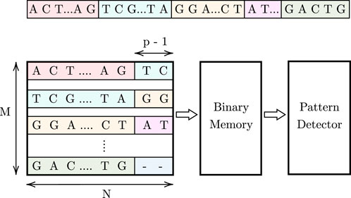
FIGURE 1. Proposed high-level design for comparing a pattern of length p =3.
Algorithm 1.Matching phase
Input: DNA data (1⋯t) and pattern P (1⋯p)
Output: Memory array mem (M, N − (p − 1))
1 AM = zeros (M, N)
2 mem = zeros (M, N − (p − 1))/* Loading data except last row */
3 c = 1
4 for i ← 1 to M − 1 do
5 AM(i, 1: N − p + 1) = data (c: c + N − p)
6 c = c + N − (p − 1)
/* Last row */
/* Remaining characters */
7 r = t − (M − 1) × (N − p + 1)
8 AM(M, 1: r) = data (t − r + 1: t)
/* Replication of characters */
9 AM(1: M − 1, N − p + 2: N) = AM(2: M, 1: p − 1)/* Dummy characters */
10 AM(M, r + 1: N) = dummy/* N-(p-1) cycles */
11 for i ← 1 to N − (p − 1) do
12 mem (1: M, i) = (AM(1: M, i: i + p − 1) = = P)
/* Run pattern detector */
13 PatternDetector(mem)
3 Hardware architecture
To perform binary and ternary search operations more efficiently, researchers have recently suggested replacing the CMOS devices in AM with memristors. More recently, the authors in (Li et al., 2020) proposed a form of memristor-based aCAM that can store a range of values, which can be matched or not to an analog input. In addition to its ability to store wide continuous intervals, an aCAM can store multiple narrow ranges as discrete levels, allowing the storage of at least 3 bits per cell. aCAM can replace digital CAM while improving both storage density and power consumption. As such, aCAM is a strong candidate for DNA pattern matching since its ability to store discrete multi-bit ranges enables the search for DNA characters.
3.1 aCAM cell
A recent study (Wang et al., 2020) compared different types of switching devices including memristors, phase change, magnetoresistors, and FeFET devices. Memristor devices have key properties, such as a high number of distinguishable states, fast switching speed, and good endurance and retention, thereby qualifying them as good candidates for aCAM applications. Several types of memristor-based aCAM have been proposed in the literature. In (Bazzi et al., 2022), the authors analyzed and compared different memristor-based aCAM cells. They found that the 8T2M cell was the most energy-efficient and offered low latency, low failure probability, and small area compared to other types of aCAMs. Thus, the 8T2M design is a suitable candidate for DNA pattern matching.
An 8T2M aCAM cell is shown in Figure 2A. The circuit is mainly divided into two voltage divider subcircuits that determine the lower and upper bounds of the stored interval, respectively, depending on the programmed resistance value in each of them. The lower-bound subcircuit consists of a transistor connected in series to a variable resistance RLB, followed by an inverter that controls the voltage VG1 at the gate of a PMOS transistor T1. The lower-bound match threshold of the aCAM cell (LB) is determined by tuning the resistance RLB. Similarly, the upper-bound match threshold (UB) is configured with an independent voltage divider using a variable resistance RUB and an inverter to generate the voltage VG2 at the gate of the pull-down NMOS transistor T2. We modified the aCAM cell such that the input for the lower-bound subcircuit VLDL is different from that of the upper-bound subcircuit VUDL, for reasons that we explain later.
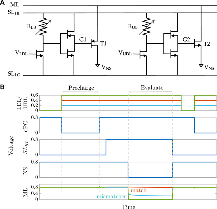
FIGURE 2. 8T2M analog CAM. (A) Schematic of the 8T2M aCAM cell. (B) Plot of the transient behavior of an 8T2M aCAM cell with match interval [0.35 V, 0.45 V] at three different LDL = UDL inputs: matching, lower-bound mismatching, and upper-bound mismatching.
An aCAM search operation consists of two phases: pre-charge and evaluate. First, the matchline (ML) is pre-charged to a high logic level through a pull-up PMOS transistor by setting its gate voltage nPC to low, as illustrated in Figure 2B. Then, the evaluation phase starts by setting the
If VLDL is less than the lower bound, a low voltage, smaller than VPC − |Vtp|, builds on G1, where VPC is the ML pre-charge voltage. This yields a mismatch because T1 will turn on and discharge the ML. On the other hand, if VUDL is greater than the upper bound, a high voltage, greater than the threshold voltage Vtn, builds on G2, turning T2 on, and the ML is discharged to a low level through T2. Thus, the ML stays high only when the search input belongs to the interval stored in the cell (match), set by the resistance values of RLB and RUB.
Figure 3 illustrates the voltage transfer characteristics for VG versus VDL. Based on these curves, for a given pair of RLB and RUB resistances, the corresponding lower and upper bounds of the stored interval can be determined based on the VDL values, which results in VG1 = VPC − |Vtp| and VG2 = Vtn.
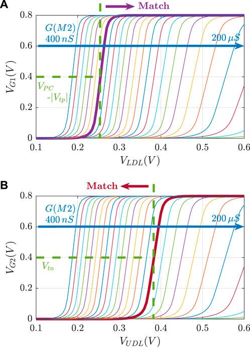
FIGURE 3. Voltage transfer characteristics VG vs. VDL for R ∈[5 kΩ, 2.5 MΩ].
3.2 DNA pattern encoding
As discussed previously, DNA sequences are combinations of four nucleotides: A, C, G, and T. Thus, if one aCAM cell stores one DNA character, four discrete levels are needed to represent the DNA characters. Using the aCAM design shown in Figure 2A, four intervals are obtained for the resistance configurations shown in Table 2. Such an encoding guarantees zero failure. Squeezing more than one character per interval would lead to some failure, especially if there was variability (Bazzi et al., 2022). A study on the performance of the aCAM cell under process variation considerations is discussed in Section 5.3. Each DNA character can be mapped into one interval defined by a lower and an upper bound, corresponding to resistances RLB and RUB, respectively (explained in Section 3.1). Figure 4 shows the transient ML voltage measured at 1 ns vs. VDL for the four intervals. Note that we added a buffer of two inverters after which we read VML, as will be discussed later. The intervals are no longer symmetric because of the gain after the inverters.
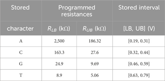
TABLE 2. Nucleotide character encoding.
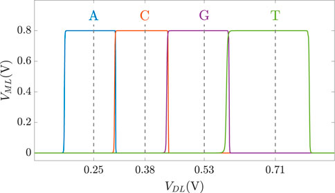
FIGURE 4. VML measured at 1 ns vs. VDL for the four DNA character intervals defined in Table 2.
3.3 Row matching
To search for a specific character in an aCAM cell, we apply to its inputs a voltage equal to the average of the lower and upper bounds of the corresponding interval defined in Table 2. The cell matches only if its stored character is equal to the one searched for.
An aCAM cell can be deactivated to give a match, regardless of its stored character, by applying to its lower-bound subcircuit a voltage VLDL = VDD and to its upper-bound subcircuit a voltage VUDL = 0. Based on Figure 3A, if the input VLDL is equal to VDD, for any resistance value in the range, the resulting VG1 is high, greater than VPC − |Vtp|, thus T1 will remain off and the lower-bound subcircuit matches. Similarly, Figure 3B shows that for an input VUDL = 0, the obtained VG2 is less than Vtn for all resistance values. Hence, T2 remains off and the upper-bound subcircuit matches. Table 3 shows the different combinations of searched and stored data that result in either a match or mismatch state. A full match occurs when all the aCAM cells match within the same row, otherwise, a mismatch is recorded, as illustrated in Figure 5. An additional interval, MM, is needed to give a mismatch for any input. This interval is stored in the extra aCAM cells of the last row of the array, as discussed earlier. We set its RLB to RUB of the last interval and its RUB to RLB of the first interval.
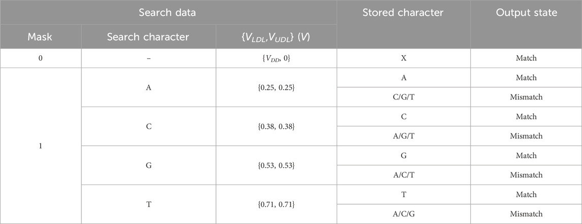
TABLE 3. Different combinations of searched and stored data that result in either a match or mismatch state. ‘X’ means don’t care.
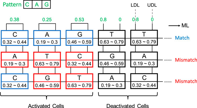
FIGURE 5. aCAM search operation example. Blue cells are matched, red cells are mismatched, and black cells are deactivated.
3.4 Proposed architecture
Figure 6 is an overview of the proposed architecture. The architecture consists of three main building blocks, as discussed earlier: (1) AM, which stores the DNA sequence, (2) match-index memory, which stores the index of the pattern matches, and (3) the pattern detector, which finds the maximum number of consecutive pattern repeats. The details of the full implementation of each block are described in this section.
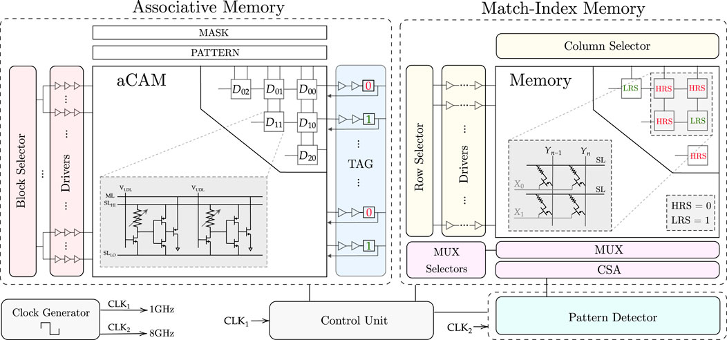
FIGURE 6. Full hardware architecture for the proposed design.
3.4.1 Associative memory
The designed AM consists mainly of three blocks: aCAM array, block selector, and tag registers.
3.4.1.1 aCAM array
The DNA data are stored in an M × N aCAM array. Since we are looking for the occurrences of a specific pattern of length equal to p, then, in our search, we activate a window of only p cells to check if this pattern exists. As the comparison can be done in parallel across the rows, p cells are activated per row in each cycle, and these are compared to the pattern. The input to the activated cells is set corresponding to the pattern characters, as defined in Table 3, whereas the aCAM cells of the deactivated columns will have VLDL set to VDD and VUDL set to 0, so that they result in a match, regardless of the characters they are storing, as discussed earlier. The window of p activated cells is shifted by 1 cell in each cycle till the end of the row, where there are special cases, since the pattern may be split between two rows. To handle these cases, we replicate (p − 1) characters. Thus, at the end of each row, we replicate and add the first (p − 1) aCAM cells from the row below it. If the DNA data are not a multiple of the row length N, the extra cells store the interval MM so that they always result in a mismatch.
3.4.1.2 Block selector
In nucleotide-repeat diseases, the location of the pattern repeats is important. In fact, for each disease, the repeats must be in a specific gene. For example, for Huntington’s disease, the CAG repeats must be in the HTT gene, which is a portion of the entire DNA sequence. To allow the detection of different diseases, we store multiple critical genes in the aCAM array. We divide the array into eight blocks, so that for each disorder, we activate the blocks containing the corresponding gene. To select or activate specific blocks, we designed a block selector. Its implementation is explained in Supplementary Note S1. The block selector activates the desired blocks by connecting its output to the aCAM cells as follows. Figure 2B shows the signaling for the 8T2M aCAM design. In the evaluate phase, VNS is set to 0. An aCAM cell can, therefore, be deactivated by keeping its VNS high during this cycle. As such, the aCAM cells of an activated block should have VNS = 0 during the evaluation, whereas those included in a deactivated block should always have VNS high. Therefore, the block selector output should be inverted before it is connected to the NS of an aCAM cell.
3.4.1.3 Drivers
The output of each block selector is connected to several chains of three inverters with an increasing width size, and their output is connected to the NS of the aCAM cells.
3.4.1.4 Tag registers
In each cycle, the ML result of each row is stored in the tag, which is written to memory. The tag consists of a buffer (two inverters) connected to a flip-flop that stores the ML value.
3.4.2 Match-index memory
In each cycle, after we have the values ready at the tag, we write them to a 1T1R memory array, so that we can later read the memory and input the values to the pattern detector to detect the patterns. The role of each 1T1R cell is to store either a low-resistive state (LRS) or a high-resistive state (HRS) corresponding to whether the pattern in the aCAM array is a match or mismatch. This is done during the memory write operation. After the array is populated, the next step is to read the array. The pattern detector counts how many consecutive patterns there are and determines the length of the sequence. After these operations are complete, we reset the memory array to HRS so that it is for the next use. The control unit generates the read, write, and reset signals to organize the sequential functions of the memory.
Each 1T1R cell consists of a memristor and an NMOS transistor, connected as shown in Figure 7. The values of the signals at each node (SL, X, and Y) vary depending on the write, read, or reset mode of the memory, as summarized in Supplementary Table S4.
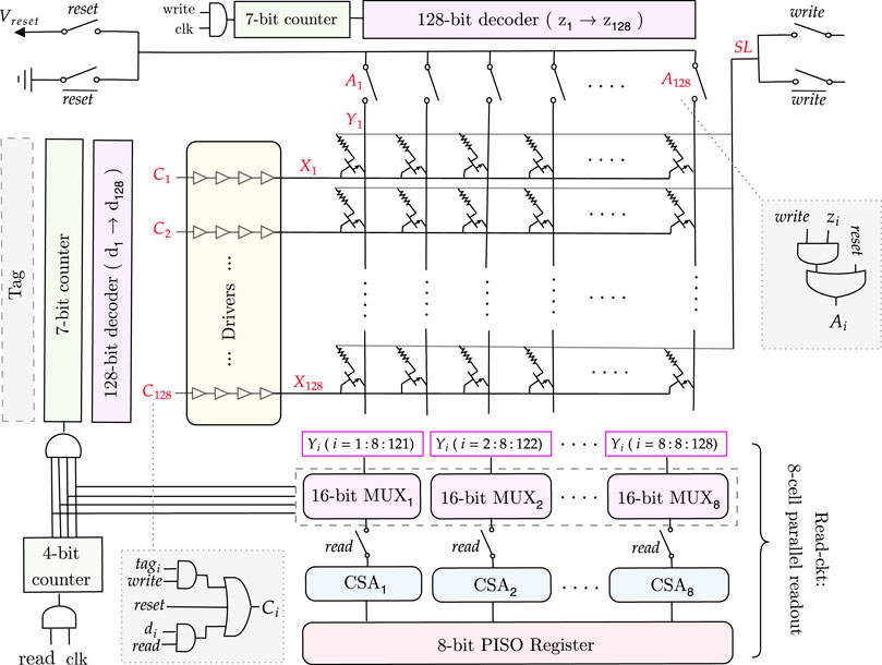
FIGURE 7. Full memory architecture for a 128×128 match-index array.
3.4.2.1 Memory write
During the memory write operation, the rows of the 1T1R memory array are filled in parallel based on the values received from the tag in each cycle. Each tag output is connected to a corresponding row (X), which is determined by the signal C, as illustrated in Figure 7. This is then followed by drivers with four inverters, which drive the current. As all rows are written in parallel, a column selector circuit is needed to write the columns (Y) of the memory array sequentially.
As shown in Supplementary Table S4, to write a column, the corresponding Y node must be 0 and all the others 1 to avoid creating a current path between Y and SL (since SL = Vset) and thus, to avoid writing them as well. To achieve this functionality, we need a counter followed by a decoder and transmission gates. In this way, the transmission gate outputs a 0 only for the targeted column that is to be written. All the other columns are high. The transmission gates are controlled by the signal A (Figure 7), which passes the ground value for the specific column chosen by the decoder (z = 1). Note that while writing the memory, the read circuitry is disconnected using the transmission gates controlled by the read signal.
For an n-column memory, the column selector circuit has a log2n-bit counter, then a log2n to n-bit decoder, followed by n transmission gates to get the desired Y value. This architecture is illustrated for a 128 × 128 memory in Figure 7.
3.4.2.2 Memory read
When all the write cycles are complete, then the 1T1R memory array is fully written. We need to read the values and input them, one by one, to the pattern detector circuit, which counts and detects the maximum sequence length. Reading the whole memory requires a row selector to traverse the rows and a multiplexer to connect the columns to a current sense amplifier sequentially to sense the stored values.
To avoid traversing the whole memory cell by cell and thus, increasing the delay, we will read every eight consecutive cells in parallel and save them in an 8-bit parallel-in serial-out (PISO) register, which will output them serially, one by one, to the pattern detector circuit. To do so, we need eight n/8-bit multiplexers, which are a chain of transmission gates whose function is to select the eight columns and connect them to the corresponding current sense amplifier. Thus, we need eight current sense amplifiers for the eight columns selected. Their output will be passed to the 8-bit PISO register, as shown in Figure 7. The selectors of the multiplexers are determined by a log2n/8-bit counter. The outputs of this counter are AND’ed and connected as the clock to the row selector circuit counter, which ensures that we read the next row only when all the current columns are read. Note that during the read operation, the column selector circuit is disconnected.
For an m × n memory array, the row selector circuit consists of a log2m-bit counter, which is followed by a log2m-to m-bit decoder, then drivers to drive the current and m transmission gates to get the desired X node value.
3.4.2.3 Memory reset
Finally, as shown in Figure 7, to reset the memory after each memory read, the columns (Y) must be connected to Vreset, SL to the ground, and the rows (X) to the reset signal to turn on the NMOS transistors and allow the current to flow from Y to SL, thus resetting the 1T1R cell to a HRS. During this mode, the column and row selectors and the read circuits are all disconnected.
3.4.3 Pattern detector
The output of the PISO register is input, bit by bit, into the pattern detector, which finds the maximum number of consecutive instances of a specific pattern. A bit equal to 1 indicates that an occurrence of the pattern was found. Thus, for patterns consisting of different characters, for example, CAG, every 1 should be followed by (p − 1) zeros. As such, whenever a 1 is received, the pattern detector can skip (p − 1) bits and check again. If the input is 1, the number of repeats is incremented. If it is a 0, the maximum is updated, and the count restarts from 0 and the sequence of inputs is traversed, bit by bit, until a new 1 is found, after which we can skip (p − 1) bits and check again. Note that for DNA pattern detection, the maximum length of a pattern consisting of different characters is 4, as there are only four nucleotides.
To generalize the pattern matching procedure to any DNA pattern, more than one pointer must traverse the sequence, because a 1 is not necessarily followed by (p − 1) zeros. Without loss of generality, for length-3 patterns, three pointers are needed to scan the inputs received from the PISO register. The first one checks the inputs having an index modulo 3 = 1. The second pointer scans the inputs with index modulo 3 = 2, and finally, the third pointer traverses the inputs with index modulo 3 = 0, as illustrated in Figure 8A. Pointer 1 starts from the first input, then it skips 2 bits to check the fourth input, and so on, and similarly for pointers 2 and 3. Each pointer has its own counter and maximum register, which saves the number of consecutive repeats.
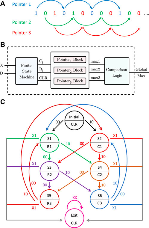
FIGURE 8. Proposed pattern detector design for length-3 patterns. (A) Three pointers traversing the sequence of memory bits. (B) Block diagram of the pattern detector. (C) State diagram of the finite state machine.
Algorithm 2.Pattern detection phase
Input: Memory array mem (m, n)
Output: GlobalMax: maximum number of consecutive pattern occurrences
1 ctr = zeros (1, p)
2 max = zeros (1, p)
3 for i ← 1 to m do
4 for j ← 1 to n do
5 idx = (i − 1) × n + j
6 x = (idx mod p)
7 if mem(i, j) == 1 then
8 ctr(x) + +
9 else
/* Update the maximum */
10 if ctr(x)
11 max(x) = ctr(x)
/* Reset the counter */
12 ctr(x) = 0
13 GlobalMax = maximum (max)
Algorithm 2 shows at a high level the pattern detection procedure for a length-p pattern. Figure 8B is a block diagram of the full pattern detector. In addition to the input X from the PISO register, another input, D, is needed so that the pattern detector can determine the end of the sequence. The pattern detector consists of a finite state machine, three pointer blocks, a comparator, and a global maximum register. The finite state machine, which takes inputs X and D, outputs the signals C and R needed for each pointer block. A clear output (CLR) is also used to reset the counters of the pointer blocks in the initial and exit states, as will be explained later. Figure 8C is a state diagram of the finite state machine. Each pointer has a block consisting of a counter, a comparator, and a maximum register. The counters are initially reset. Whenever a 1 is received from the PISO, the counter of the corresponding pointer is incremented by 1 (C = 1), whereas if the input is 0, the corresponding maximum register is compared to the counter value and updated if needed, and the counter is then reset (R = 1). When the sequence ends, indicated by the D input, all the counters are reset and the maximum of the three maximum registers is found and stored in the global maximum register.
As an example, let us assume that the input sequences for X and D are “1 0 1 1 1 0 0 0 0” and “0 0 0 0 0 0 0 0 1”, respectively. Table 4 shows the current state starting from the initial state and each subsequent state depending on the input xD, along with the required action in that state. The last state is the exit state, which returns the global maximum.
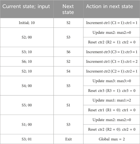
TABLE 4. Pattern detector actions based on the example input sequence.
3.4.4 Control unit
The role of the control unit is to generate the control signals required by each block of the full architecture to organize the phases and ensure the correct sequential flow of the data. For example, it generates the read, write, and reset signals in the match-index memory depending on the different memory modes to ensure the operations are correct. The control unit can be realized on software running on a coprocessor. Hence, we have not discussed its circuit implementation.
3.5 Timing considerations
When an input equal to 0 is received from the PISO register, two actions need to be done: (1) comparing and updating the maximum register and (2) resetting the counter of the corresponding pointer. It is important to separate the comparison and reset steps in time to ensure that the comparison happens before the counter is reset. Since every pointer is activated every three cycles, we delayed the comparison by one clock cycle and the reset by two clock cycles, so that both are completed before the same pointer hits another input. When the sequence of bits is finished, the pattern detector should read four extra zeros to ensure that all the maximum registers are updated. An additional 0 is needed to move it to the exit state, when all the counters are reset and the three maximum registers are compared to determine the maximum among them. Hence, we delayed the end of the sequence signal by four clock cycles. Since the reset is delayed by two clock cycles, we used the CLR signal, which we set to 1 in the initial and exit states so that the counters are reset in those states.
Two clocks are needed for the pattern matching task. The first clock, operating with a period T, is utilized for the (M × N) AM pattern search and (m × n) memory write. On the other hand, the faster clock, with a period T/8, is used for memory read and pattern detection. For loading the DNA data into AM, the aCAM cells can be programmed row by row. Consequently, cells storing the same character within the same row can be programmed simultaneously. As there are four DNA characters and two memristors in each aCAM cell, the time required to load each row is 8Tw, where Tw is the memristor write time. Therefore, loading data into M rows takes t1 = 8MTw. Note that loading the data is done only once. For each block in the aCAM array, memory write can occur in parallel with the pattern search phase, starting after one clock cycle. To enhance speed and efficiency, a pipelined architecture is employed. Two match-index memories are used, allowing the reading of one memory while writing the results of new pattern search operations into the other memory. This process begins from the second AM block, where reading the memory of the previous block can occur simultaneously with the pattern search of the next block. The pattern detection starts one clock cycle after reading from memory, and its operation is continuous across all processing blocks. Finally, resetting each memory is done in one clock cycle. Hence, for the first block only, the time needed is the time for pattern search plus one cycle, which is equal to T (N − (p − 1) + 1), whereas for the following blocks, it is dominated by the memory read, which is equal to
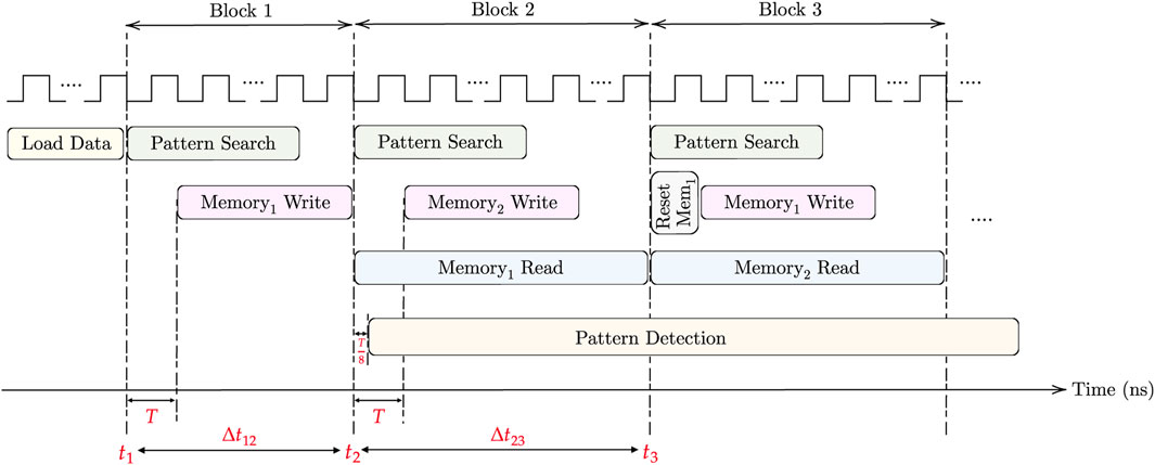
FIGURE 9. Timing diagram for the proposed design.
where T represents the period of CLK1, D is the additional delay needed by the pattern detector to finalize its operation, which is equal to 6 (T/8) in the case of 3-length pattern, and ts,k denotes the total time needed to return the maximum number of consecutive pattern repeats in K blocks. It should be noted that during the last block cycle, a pattern search operation is not performed.
4 Experimental setup
We built a simulation framework with MATLAB and HSPICE for both circuit and system simulations. In the circuit simulations, we relied on predictive technology models for 45-nm high-k/metal gate CMOS devices (Cao, 2018) to study the design metrics. We set VDD = 0.8 V. We considered the HTT gene as a case study for evaluating the proposed design.
The AM has a block selector, drivers, aCAM array, and tag. We implemented the block selector using CMOS gates, as explained in Supplementary Note S1. The output of each block selector is connected to 64 drivers with three inverters each, which are connected to the rows of the aCAM array. We used a 512 × 130 aCAM array to store the DNA data, which we divided into eight blocks, each consisting of 64 rows. The ML of each row is connected to a driver with two inverters, followed by a flip-flop that stores the ML result.
In our memory simulations, we adopted a linear memristor model, parameterized with the data reported in (Li et al., 2020; Pedretti et al., 2021). We studied a 64 × 128 memory array. Accordingly, the memory components were as follows. For a write operation to a 64 × 128 memory array, the column selector circuit has a 7-bit counter, then a 7 to 128-bit decoder followed by 128 inverters and 128 transmission gates. To read the memory, the row selector circuit consists of a 6-bit counter, followed by a 6 to 64-bit decoder, then 64 transmission gates. To read every eight consecutive cells in parallel, we used eight 16-bit multiplexers connected to eight current sense amplifiers, whose outputs are passed to an 8-bit PISO register. The circuit connections are as shown in Figure 7. For the column and row selector circuits, we used synchronous master–slave JK-flip-flop up counters to minimize the delays and avoid glitches. For the current sense amplifier, we used the circuit presented in (Sun et al., 2018). We modified the Ron, Roff, and Rref parameters to meet the specifications of our circuit: Ron = 5 kΩ, Roff = 2.5 MΩ, and Rref = 14 kΩ. For the pattern detector, first, for the finite state machine, we used dynamic flip-flops to represent the states, which enhanced performance and speeded up the latching. Then, for each pointer block, we used an 8-bit D-flip-flop counter, an 8-bit comparator, and an 8-bit maximum register, as shown in Supplementary Figure S2 in Supplementary Note S2. The comparison logic, which returns the maximum value among all the maximum registers, was implemented using two 8-bit comparators, two multiplexers, and an 8-bit global maximum register, which stores the global maximum, as illustrated in Supplementary Figure S3 in Supplementary Note S2.
5 Results and discussion
In this section, we evaluate the performance of our circuit in terms of key metrics, namely, latency, energy, and area.
First, for the delay, we set the clock cycle T to 1 ns based on the circuit simulations. By applying the time equations in the timing considerations under Section 3.5 and based on Figure 9, assuming Tw = 1 cycle, the amount of overhead needed to load the data into the aCAM array is t1 = 8 MT = 4.096 μs. The time needed to process the first block is Δt12 = 129 ns. Whereas for the other blocks, it is equal to Δt23 = 1,024 ns. As such, in total, ignoring the time overhead to load the data and applying Eq. 1d, the pattern matching task for one aCAM array storing 512 × 128 DNA characters takes around 8.322 μs.
Energy values were obtained from simulations, except for writing the memory, since we adopted a linear resistor model, so we assumed that the memristor SET energy is 1 pJ. We also assumed that the reset energy is the same as the write energy since all the SET cells need to be reset. In total, the pattern matching task for an aCAM array consisting of eight blocks consumes 41.79 nJ. Note that we did not include the data storage energy since the write operation is usually done once and the search is performed many times. Figure 10 shows the distributions of the energy among the different operations.
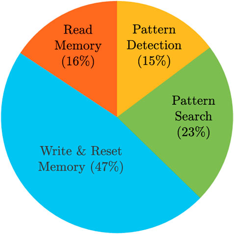
FIGURE 10. Energy breakdown for the proposed hardware accelerator storing/searching 512×128 DNA characters.
The active area was estimated based on the transistors count and size as follows. Initially, we computed the transistor area using the conventional NMOS transistor layout (Saman, 2017), resulting in an individual transistor area of 4λ × 10λ = 40λ2. To account for the spacing between transistors, we added 2λ to each side, which results in an estimated area equal to 112λ2. In our simulations, we used 45 nm technology with a transistor length of 45 nm (2λ = 45 nm), and we sized the NMOS and PMOS transistors differently. Subsequently, we calculated the estimated area for each proposed block design based on the number of NMOS and PMOS transistors and their respective widths. The resulting estimated active area values are based on the following equation:
Where W represents the sum of the widths of all transistors in the circuit, and n is the number of transistors. Consequently, the calculated areas for each block, including its peripherals, are as follows: the AM area is 0.0463 mm2, the match-index memory area is 3,053.18 μm2, and the pattern detector area is 622.54 μm2. Hence, the total area of the proposed design is 0.05 mm2.
5.1 Performance comparison to related work
To assess the efficiency of the proposed design, we compared its performance against existing works in the literature that utilize general-purpose accelerators (Raju et al., 2018). We evaluated the execution time required for the DNA pattern matching task across different DNA sequence lengths: 10, 50, and 100 Mb. The results show a significant improvement achieved by our design, as illustrated in Figure 11. Unlike general-purpose accelerators, our design incorporates a domain-specific ReRAM-based hardware accelerator specifically for implementing a hardware-friendly pipelined algorithm for DNA pattern matching. This results in remarkable performance improvements. In comparison to existing methods, our design exhibited a significant enhancement, with execution time improvements of 104×, 155×, and 140× for DNA sequence lengths of 10, 50, and 100 Mb, respectively. These results prove the significant acceleration that our proposed accelerator design brings to the DNA pattern matching technique.
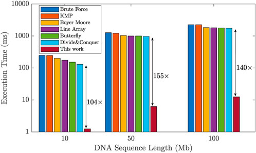
FIGURE 11. Improvement of the proposed design in terms of DNA pattern matching execution time with respect to prior works, for different sequence lengths.
5.2 Effect of pattern length
To determine the effect of increasing the pattern length on run time and energy, we consider the example of a DNA sequence of 1 million characters. For a pattern of length 3, there are two replicated cells in each row, so 16 (512 × 130) aCAM arrays are needed to store the DNA data, each consisting of 8 blocks. In this case, ignoring the time overhead in Eq. 1d, the total run time for the pattern matching task is 131.2 μs. On the other hand, for a pattern of length p = 5, we still need 16 aCAM arrays, however, in this case, there are four replicated cells in each row, hence 126 search cycles are needed instead of 128. The total run time is 129.15 μs.
Moreover, we estimated the energy per cycle for each component in our design based on our simulations. For each pattern length, we multiplied the energy values per cycle by the corresponding number of cycles needed to perform the pattern matching task on the aCAM blocks storing 1 million DNA characters. Accordingly, for p = 3, the total energy is 668.6 nJ, whereas for p = 5, it is 661.2 nJ.
5.3 Impact of process variations
We studied the impact of process variation on the performance of the proposed design by introducing process variations to the threshold voltages of the transistors. Specifically, NMOS devices were subject to a 3σvt of ∼50 mV variation, while PMOS devices were subject to a 3σvt of ∼30 mV variation. Additionally, we considered variability in memristor resistances where we set 3σ/μ to up to 10%. To assess the effect of variability on the design, we used the failure probability in the match operation as a characterization metric. We performed 1,000 Monte Carlo SPICE simulations for a row of 130 cells, with 3 cells activated to search for a pattern of length 3, and measured VML for both full match and 1 mismatch cases in each simulation run. We identified the optimal reference voltage value, Vref, that maximizes the separation between match and mismatch scenarios in the presence of variability. The failure probability is defined based on the number of match and mismatch failures, corresponding to simulations with a match value below Vref and simulations with a mismatch value above Vref, respectively. The results show that the 8T2M cell is robust against variability, achieving zero failure for the studied variations.
6 Conclusion
In this paper, we present a hardware accelerator design for exact DNA pattern matching. The proposed architecture utilizes associative memory to store DNA characters and implements a highly parallelized hardware-friendly algorithm for acceleration. The algorithm counts the maximum number of consecutive repeats of a specific pattern, which can be used to detect the presence of possible trinucleotide repeat-expansion genetic disorders. Our proposed design is energy-efficient, and it showed more than 100× improvement in terms of time cost compared to existing software implementations of DNA pattern matching. It is noteworthy that, in the presence of DNA sequencing errors, we can explore techniques such as approximate matching as an alternative to exact matching, which is a subject for future work.
Data availability statement
The original contributions presented in the study are included in the article/Supplementary Material, further inquiries can be directed to the corresponding author.
Author contributions
MF: Conceptualization, Formal Analysis, Investigation, Methodology, Project administration, Supervision, Writing–review and editing. JB: Conceptualization, Data curation, Investigation, Methodology, Software, Validation, Writing–original draft. JS: Investigation, Validation, Writing–original draft. RK: Methodology, Project administration, Supervision, Writing–review and editing. AE: Supervision, Writing–review and editing.
Funding
The author(s) declare that no financial support was received for the research, authorship, and/or publication of this article.
Conflict of interest
Author MF was employed by Rain Neuromorphics Inc. Author RK was employed by Synopsys Inc.
The remaining authors declare that the research was conducted in the absence of any commercial or financial relationships that could be construed as a potential conflict of interest.
Publisher’s note
All claims expressed in this article are solely those of the authors and do not necessarily represent those of their affiliated organizations, or those of the publisher, the editors and the reviewers. Any product that may be evaluated in this article, or claim that may be made by its manufacturer, is not guaranteed or endorsed by the publisher.
Supplementary material
The Supplementary Material for this article can be found online at: https://www.frontiersin.org/articles/10.3389/felec.2023.1343612/full#supplementary-material
References
Adey, S. P. (2013). Gpu accelerated pattern matching algorithm for dna sequences to detect cancer using cuda dissertation. Coll. Eng. Pune.
Adjeroh, D., Zhang, Y., Mukherjee, A., Powell, M., and Bell, T. (2002). “Dna sequence compression using the burrows-wheeler transform,” in Proceedings. IEEE computer society bioinformatics conference (IEEE), 303–313.
Arsovski, I., Chandler, T., and Sheikholeslami, A. (2003). A ternary content-addressable memory (tcam) based on 4t static storage and including a current-race sensing scheme. IEEE J. Solid-State Circuits 38, 155–158. doi:10.1109/jssc.2002.806264
Bazzi, J., Sweidan, J., Fouda, M. E., Kanj, R., and Eltawil, A. M. (2022). Efficient analog cam design. arXiv preprint arXiv:2203.02500.
Boyer, R. S., and Moore, J. S. (1977). A fast string searching algorithm. Commun. ACM 20, 762–772. doi:10.1145/359842.359859
Cao, Y. (2018). Ptm. Available at: http://ptm.asu.edu/.
Cormen, T. H., Leiserson, C. E., Rivest, R. L., and Stein, C. (2022). Introduction to algorithms. MIT press.
Fouda, M. E., Yantır, H. E., Eltawil, A. M., and Kurdahi, F. (2022). “In-memory associative processors: tutorial, potential, and challenges,” in IEEE transactions on circuits and systems II: express briefs.
Garzón, E., Golman, R., Jahshan, Z., Hanhan, R., Vinshtok-Melnik, N., Lanuzza, M., et al. (2022). Hamming distance tolerant content-addressable memory (hd-cam) for dna classification. IEEE Access 10, 28080–28093. doi:10.1109/access.2022.3158305
Hakak, S. I., Kamsin, A., Shivakumara, P., Gilkar, G. A., Khan, W. Z., Imran, M., et al. (2019). Exact string matching algorithms: survey, issues, and future research directions. IEEE Access 7, 69614–69637.
Kaplan, R., Yavits, L., and Ginosar, R. (2018). Rassa: resistive prealignment accelerator for approximate dna long read mapping. IEEE Micro 39, 44–54. doi:10.1109/mm.2018.2890253
Khatamifard, S. K., Chowdhury, Z., Pande, N., Razaviyayn, M., Kim, C. H., and Karpuzcu, U. R. (2021). Genvom: read mapping near non-volatile memory. IEEE/ACM Trans. Comput. Biol. Bioinforma. 19, 3482–3496. doi:10.1109/tcbb.2021.3118018
Kim, J. S., Senol Cali, D., Xin, H., Lee, D., Ghose, S., Alser, M., et al. (2018). Grim-filter: fast seed location filtering in dna read mapping using processing-in-memory technologies. BMC genomics 19, 89–40. doi:10.1186/s12864-018-4460-0
Kim, Y., Imani, M., Moshiri, N., and Rosing, T. (2020). Geniehd: Efficient dna pattern matching accelerator using hyperdimensional computing, in 2020 Design, Automation & Test in Europe Conference & Exhibition (DATE) (IEEE), 115–120.
Knuth, D. E., Morris, J. H., and Pratt, V. R. (1977). Fast pattern matching in strings. SIAM J. Comput. 6, 323–350. doi:10.1137/0206024
Kokosiński, Z., and Sikora, W. (2002). “An fpga implementation of a multi-comparand multi-search associative processor,” in International conference on field programmable logic and applications (Springer), 826–835.
Laguna, A. F., Gamaarachchi, H., Yin, X., Niemier, M., Parameswaran, S., and Hu, X. S. (2020). “Seed-and-vote based in-memory accelerator for dna read mapping,” in 2020 IEEE/ACM international conference on computer aided design (ICCAD) (IEEE), 1–9.
Lalonde, E., Rentas, S., Lin, F., Dulik, M. C., Skraban, C. M., and Spinner, N. B. (2020). Genomic diagnosis for pediatric disorders: revolution and evolution. Front. Pediatr. 8, 373. doi:10.3389/fped.2020.00373
Lei, S., Wang, C., Fang, H., Li, X., and Zhou, X. (2016). Scadis: a scalable accelerator for data-intensive string set matching on fpgas, in 2016 IEEE Trustcom/BigDataSE/ISPA (IEEE), 1190–1197.
Li, C., Graves, C. E., Sheng, X., Miller, D., Foltin, M., Pedretti, G., et al. (2020). Analog content-addressable memories with memristors. Nat. Commun. 11, 1638–8. doi:10.1038/s41467-020-15254-4
Mahmud, P., Rahman, A., Hasan Talukder, K., et al. (2023). An improved hashing approach for biological sequence to solve exact pattern matching problems. Appl. Comput. Intell. Soft Comput.
Markić, I., Štula, M., Zorić, M., and Stipaničev, D. (2020). Entropy-based approach in selection exact string-matching algorithms. Entropy 23, 31.
Mane, S. U., and Pangu, K. H. (2016). “Disease diagnosis using pattern matching algorithm from dna sequencing: a sequential and gpgpu based approach,” in Proceedings of the international conference on Informatics and analytics, 1–5.
Paulson, H. (2018). Repeat expansion diseases. Handb. Clin. neurology 147, 105–123. doi:10.1016/B978-0-444-63233-3.00009-9
Pedretti, G., Graves, C. E., Serebryakov, S., Mao, R., Sheng, X., Foltin, M., et al. (2021). Tree-based machine learning performed in-memory with memristive analog CAM. Nat Commun. 12 (1), 5806. doi:10.1038/s41467-021-25873-0
Raju, S. V., Reddy, K., and Rao, C. S. (2018). Parallel string matching with linear array, butterfly and divide and conquer models. Ann. Data Sci. 5, 181–207. doi:10.1007/s40745-017-0124-1
Saman, B. (2017). Modeling of multi-state spatial wavefunction switched (sws) fets for logic gates and memories.
Sun, X., Yin, S., Peng, X., Liu, R., Seo, J.-s., and Yu, S. (2018). “Xnor-rram: a scalable and parallel resistive synaptic architecture for binary neural networks,” in 2018 design, automation test in europe conference exhibition (DATE), 1423–1428. doi:10.23919/DATE.2018.8342235
Usdin, K. (2008). The biological effects of simple tandem repeats: lessons from the repeat expansion diseases: Table 1. Genome Res. 18, 1011–1019. doi:10.1101/gr.070409.107
Wang, Z., Wu, H., Burr, G. W., Hwang, C. S., Wang, K. L., Xia, Q., et al. (2020). Resistive switching materials for information processing. Nat. Rev. Mater 5, 173–195. doi:10.1038/s41578-019-0159-3
Keywords: DNA sequencing, disease diagnosis, pattern matching, associative memory, analog CAM (aCAM)
Citation: Bazzi J, Sweidan J, Fouda ME, Kanj R and Eltawil AM (2024) Hardware acceleration of DNA pattern matching using analog resistive CAMs. Front. Electron. 4:1343612. doi: 10.3389/felec.2023.1343612
Received: 23 November 2023; Accepted: 21 December 2023;
Published: 12 February 2024.
Edited by:
Angela Slavova, Bulgarian Academy of Sciences (BAS), BulgariaReviewed by:
Esteban Garzón, University of Calabria, ItalyAngela Slavova, Bulgarian Academy of Sciences (BAS), Bulgaria
Copyright © 2024 Bazzi, Sweidan, Fouda, Kanj and Eltawil. This is an open-access article distributed under the terms of the Creative Commons Attribution License (CC BY). The use, distribution or reproduction in other forums is permitted, provided the original author(s) and the copyright owner(s) are credited and that the original publication in this journal is cited, in accordance with accepted academic practice. No use, distribution or reproduction is permitted which does not comply with these terms.
*Correspondence: Mohammed E. Fouda, foudam@uci.edu