Effects of Film Thickness and Coating Techniques on the Photoelectrochemical Behaviour of Hematite Thin Films
 Pannan I. Kyesmen
 Nolwazi Nombona
 Mmantsae Diale
- 1Department of Physics, University of Pretoria, Pretoria, South Africa
- 2Department of Chemistry, University of Pretoria, Pretoria, South Africa
In this research, three different sets of hematite (α-Fe2O3) films of various thicknesses were prepared using dip, spin, and combined dip/spin coating methods. α-Fe2O3 films of 450–500, 740–800 and 920–980 ± 30 nm thicknesses were prepared using each of the coating methods, and their photoelectrochemical (PEC) behaviour was investigated. Dip coated films produced the best photoresponse while the films prepared using the spin coating method yielded the least photocurrent values across films of different thicknesses. Maximum photocurrent densities of 34.6, 7.8, and 13.5 μA/cm2 V vs reversible hydrogen electrode (RHE) were obtained for the dip, spin and combined dip/spin coated films with a thickness of 740–800 ± 30 nm respectively. Improved crystallization, low charge transfer resistance at the α-Fe2O3/electrolyte interface, high surface states capacitance and the more negative flat band potential values obtained for dip coated films have been associated with the enhanced photocurrent response recorded for the films. The preferential crystal growth of spin coated films in the (104) plane associated with low electron mobility and the high resistance to charge transfer at the α-Fe2O3/electrolyte interface of the films is largely responsible for their low photoresponse. This study underscores the significance of simultaneously optimizing both coating techniques for film deposition and the film’s thickness in preparing nanostructured α-Fe2O3 films for PEC applications.
Introduction
α-Fe2O3, the most stable phase of iron oxide has found applications in numerous fields including gas sensing (Hjiri, 2020), medicine (Rajendran et al., 2015; Naz et al., 2019), magnetic recording (Jalli et al., 2010), and PEC water splitting (Kim et al., 2013; Feng et al., 2020; Reddy et al., 2020). The use of α-Fe2O3 as a photoanode for PEC water splitting has been broadly investigated in recent times because of its suitable properties such as low bandgap of ∼2.0 eV, stability in aqueous solution, availability, non-toxicity to the environment and low cost. Nonetheless, the efficiency of α-Fe2O3 in PEC water splitting is not yet close to the theoretically predicted limit of 17% (Dias et al., 2016). The shot hole diffusion length of (2–4) nm (Kim et al., 2013) for α-Fe2O3 which results in high recombination rate of electron-hole pairs during PEC applications is among the top challenges limiting its efficiency. Nanostructuring is one of the approaches that have been utilized in mitigating the effects of shot hole diffusion length on the PEC performance of α-Fe2O3 films (Tamirat et al., 2016). Nanostructured α-Fe2O3 photoanode provides increased solid-electrolyte interfacial surface area for water oxidation, suitable for charge carriers transport and separation (Tamirat et al., 2016; Khakpour et al., 2018). Nanostructured α-Fe2O3 films have been prepared using different methods such as the chemical vapour deposition (Kim et al., 2013), solution-based colloidal technique (Sivula et al., 2010; GonçAlves et al., 2011), RF sputtering (Feng et al., 2020), and spray pyrolysis (Kant et al., 2018). The solution-based colloidal method is one of the inexpensive and scalable approaches used in preparing nanostructured α-Fe2O3 films for photocatalytic applications (Sivula et al., 2010). The method requires the deposition of the precursor solution onto a substrate which is done using techniques such as drop casting, spin coating and dip coating among others. Among these techniques, the dip and spin coating methods have been widely used for depositing α-Fe2O3 thin films for PEC water splitting (Souza et al., 2009; Bora et al., 2011; GonçAlves et al., 2011; Lee et al., 2014).
Previously, the impact of coating techniques on the structural and optical properties of nanostructured thin films have been investigated. Improved crystallization has been reported for Tungsten oxide (WO3) films prepared via the dip coating method over the spin coated ones (Deepa et al., 2006). Coating techniques were found to also impact the absorption pattern and crystallization of α-Fe2O3 films prepared using the dip, spin and combined dip/spin coating method. Dip coated α-Fe2O3 films recorded the highest crystal size value while the spin coated films yielded the least values (Kyesmen et al., 2019). Higher crystallization of α-Fe2O3 films can reduce the number of grain boundaries in the films leading to the reduction in the number of electrons scattering centers, lowering their resistivity, thereby improving photocatalytic efficiency (Schuler and Aegerter, 1999). Also, the α-Fe2O3 films prepared using the combined dip/spin coating technique showed higher absorption in the visible region at wavelengths below 500 nm compared to the spin coated films irrespective of having lower film thickness. Increased absorption can result in improvement in the number of photogenerated electron-hole pairs which can enhance PEC response (Wang and Turner, 2010). Thus, coating techniques can affect the crystallization as well as absorption pattern of α-Fe2O3 films which can have significant effect on their PEC response when used as a photocatalyst for water splitting.
Another important parameter that can affect the PEC properties of α-Fe2O3 photoanodes is the film’s thickness. Hematite films require films of over 400 nm thickness for effective photon absorption for PEC applications because of its low absorption coefficient (Sivula et al., 2011). On the other hand, due to the short hole diffusion length of α-Fe2O3 (2–4 nm) (Ahn et al., 2014), photogenerated charge carriers in the bulk of α-Fe2O3 films that are too thick will likely recombine before getting to the surface of the films to perform water oxidation. Nanostructured α-Fe2O3 films that are thick enough to absorb sufficient photons can also offer a large interfacial area for interaction with the electrolyte, promoting charge carriers transport during photocatalytic reactions. Therefore, controlling the film thickness of α-Fe2O3 is important for optimizing it’s PEC efficiency (Vanags et al., 2015). Studies that simultaneously examines the effect of both film thickness and deposition techniques on the photocatalytic properties of α-Fe2O3 films have been sparsely presented in literature. Such studies are capable of yielding a better perspective on the influence of both film thickness and deposition techniques on the photocatalytic properties of the films compared to when the investigations are done separately on the individual parameters.
In this research, three different sets of α-Fe2O3 films were prepared using dip, spin, and combined dip/spin coating techniques and their PEC properties were investigated. α-Fe2O3 films of 450–500, 740–800 and 920–980 ± 30 nm thicknesses were prepared using each of the coating methods respectively, to get a better perspective on the influence of both coating techniques and film thickness on the PEC behaviour of the films. Similar film thicknesses were achieved for each set of films produced by the different coating methods through the optimization of the withdrawal rate and rotation speed for dip and spin coated layers respectively. Maximum photocurrent density of 34.6 μA/cm2 V vs RHE was obtained for dip coated films with the thickness of 740–800 ± 30 nm while the samples prepared using the spin coating technique yielded the least photo response across films of different thicknesses. This study highlights the importance of simultaneously optimizing both the coating techniques for film deposition and the film’s thickness when preparing nanostructured α-Fe2O3 films for PEC water splitting.
Experimental Methods
Films Preparation
The precursor solution of an iron oleate complex used for film deposition was obtained as described in our previous report (Kyesmen et al., 2019). FTO substrates of size 3.1 × 1.1 cm were first cleaned using a previously described procedure (Lee et al., 2014). Using the precursor solution prepared, α-Fe2O3 films were deposited on FTO substrates by dip, spin and combined dip/spin coating techniques. The precursor solution obtained was used to deposit α-Fe2O3 films on FTO using dip, spin and combined dip-spin coating methods. For dip coating, the FTO substrates were dipped for 2 min in the precursor, removed at a withdrawal speed of 30 mm/min, dried for 15 min at 70°C and annealed for 30 min at 500°C. The process was repeated thrice to obtain four layers of dip coated α-Fe2O3 films and the samples were denoted as D30. To obtain dip coated films of increased thickness, additional samples were prepared at 60 and 110 mm/min while maintaining all other experimental conditions and labelled as D60 and D110 respectively. In the spin coating process, few drops of the precursor complex were dropped on the substrate, made to spin for 30 s at 4000 rpm, dried/annealed under the same conditions as the dip coated films. The process was also repeated thrice to obtain four layers of spin coated α-Fe2O3 films on FTO substrate and labelled as S4000. In order to obtain spin coated films of increased thickness, additional samples were prepared at 900 and 600 rpm while maintaining all other experimental conditions and labelled as S900 and S600 respectively. Lastly, another three sets of samples were prepared using the combined dip/spin coating method consisting of two spin coated layers between dip coated ones. The first film was made with the two layers of spin coated films prepared at 4,000 rpm rotation speed while the dip coated layers were deposited at 30 mm/min withdrawal rate and labelled as C30. The second sample was prepared with the two spin coated layers prepared at the rotation speed of 900 rpm, while the dip coated films was made at the withdrawal rate of 60 mm/min and labelled as C60. Finally, the two spin coated layers of the third film were prepared at the rotation speed of 600 rpm, while its dip coated layers were made at 110 mm/min withdrawal rate and labelled as C110. The films were dried/annealed under the same conditions as described for the other films. Figure 1A–C presents an illustration that summarizes the rotation speeds and/or withdrawal rates used while preparing the different layers of dip, spin and dip/spin coated samples respectively.
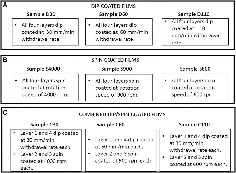
FIGURE 1. An illustration summarizing the rotation speeds and/or withdrawal rates used while preparing the different layers of (A) dip, (B) spin and (C) dip/spin coated samples respectively.
Characterization
X-ray diffraction (XRD) studies were performed on the prepared α-Fe2O3 films to investigate their structural properties using Bruker D2 PHASER-e diffractometer of Cu-Kα radiation at 0.15418 nm wavelength. Field emission gun scanning electron microscopy (FEG-SEM) conducted using the Ultrafast 540 instrument to obtain the cross-sectional images of the films. ImageJ software was employed in analyzing the cross-sectional micrographs of the films to obtain their approximate thicknesses.
A three-electrode PEC cell having a quartz window and coupled to a VersaSTAT 3F potentiostat from Princeton Applied Research was used to investigate the electrochemical behaviour of the films. 1 M NaOH (pH of 13.6) was used as the electrolyte while silver/silver chloride (Ag/AgCl) in 3M KCl, platinum meshed wire of 2 × 2 cm dimension and FTO/α-Fe2O3 films were used as the reference, counter and working electrodes respectively. About 1.80 cm2 surface area of α-Fe2O3 photoanode was dipped into the electrolyte and linear sweep voltammetry (LSV) were performed in dark and under illumination conditions at a scan rate of 0.05 V/s to extract the photocurrent response of the films. The Newport Oriel® LCS −100™ solar simulator was utilized as the light source, a Newport 91150 V reference cell was employed to calibrate the solar simulator to 1 Sun and the surface area of the photoanode exposed to light was 0.49 cm2. EIS measurements of the photoanodes were performed at 0.23 V vs Ag/AgCl, in the frequency range of 10, 000–0.1 Hz at an amplitude of 10 mV, in dark and under illumination conditions. ZView software was engaged in fitting the raw data collected from the EIS measurements to a modelled equivalent circuit. M-S measurements of the photoanodes were performed in dark at a fixed frequency of 1000 Hz, in the potential range of −1.2 to 0.5 V and an amplitude of 10 mV.
The potential values in Ag/AgCl reference utilized for all the electrochemical measurements were converted to the RHE scale using the Nernst relation in Eq. 1:
where,
Results and Discussion
Surface Morphology and Film Thickness
The surface morphology of the films prepared using the different coating methods are presented in Figures 2A–I for samples D30, D60, D110, S4000, S900, S600 C30, C60 and C110, respectively. All the films revealed spherical nanoparticles and many agglomerations into larva-shaped nanostructures. The surface of all the dip coated samples (Figures 2A–C) appeared to be less uniform compared to spin and combined dip/spin coated films. The inset of Figures 2A–I shows the histogram of the particle size distribution of along the diameter of the nanoparticles for all the samples. The particle sizes estimated for the films ranged from 28.5 to 34.0, 26.9 to 29.7 and 27.9 to 30.3 nm with standard deviation (S.D) values of 3.5–5.7, 2.7–4.8, and 3.8–4.1 nm for dip, spin and combined dip/spin coated films respectively. The maximum particle size of 34.0 nm was estimated for dip coated sample D60 while sample S4000 prepared via the spin coating method yielded the least size of 26.9 nm. Increase in the particle size of hematite films can lead to the reduction of grain boundaries, promote charge transport and PEC performance of hematite films (Tamirat et al., 2016).
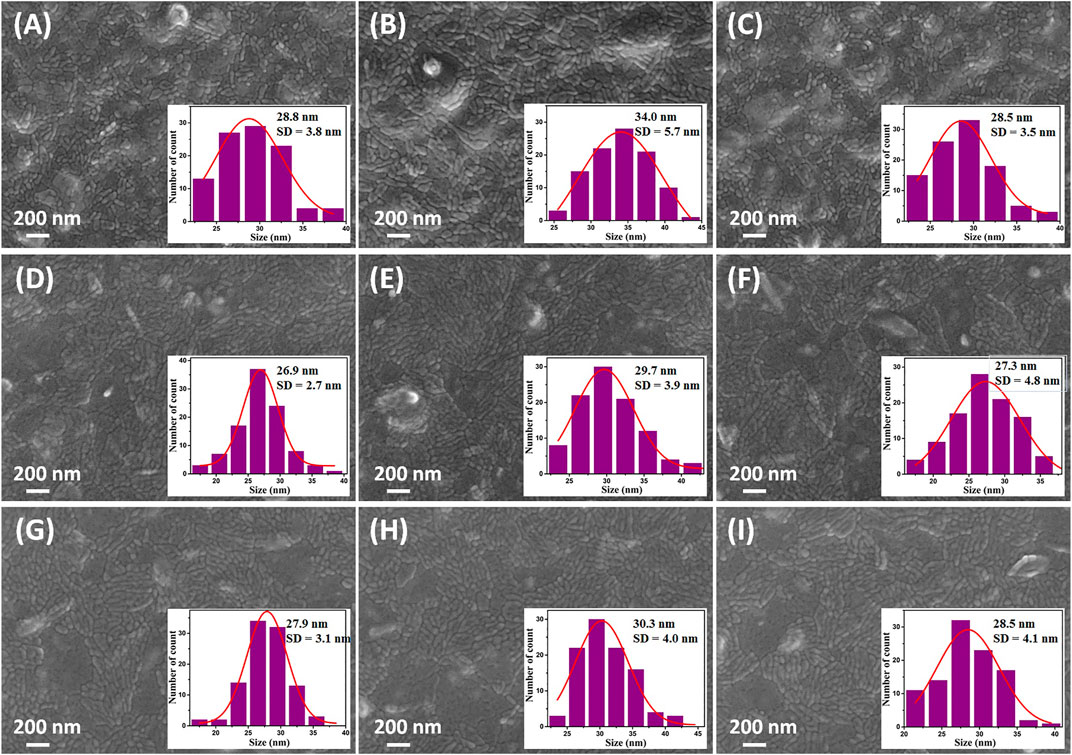
FIGURE 2. FE-SEM surface morphology of samples (A) D30 (B) D60 and (C) D110 prepared using dip coating and (D) S4000 (E) S900 and (F) S600 for spin coated films and (G) C30 (H) C60 and (I) C110 fabricated via the combined dip/spin coating techniques respectively.
The cross-sectional views of the dip, spin and combined dip/spin coated films consisting of three samples for each of the coating technique used for film deposition are presented in Figure 3. Films prepared via the dip coating method revealed film thicknesses of 458 ± 43, 789 ± 42 and 924 ± 32 nm for samples D30, D60 and D110, presented in Figures 3A–C respectively. The films produced using the spin coating technique yielded films with thicknesses of 482 ± 53, 771 ± 35 and 941 ± 37 nm for samples S4000, S900 and S600, and given in Figures 3D–F respectively. Lastly, the films produced using the combined dip/spin coating approach disclosed film thicknesses of 473 ± 40, 750 ± 42 and 968 ± 47 nm for samples C30, C60 and C110, presented in Figures 3G–I respectively. Generally, samples with approximate film thicknesses in the range of 450–500 ± 30 nm, 740–800 ± 30 nm and 920–980 ± 30 nm were prepared using each of the coating methods respectively. The films were made to have similar thicknesses for each set of samples prepared using the different coating methods, through the optimization of the withdrawal rate and rotation speed for dip and spin coated layers respectively.
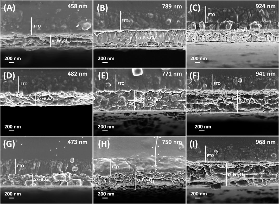
FIGURE 3. FE-SEM cross-sectional views of samples (A) D30 (B) D60 and (C) D110 prepared using dip coating and (D) S4000 (E) S900 and (F) S600 for spin coated films and (G) C30 (H) C60 and (I) C110 fabricated via the combined dip/spin coating techniques respectively.
The withdrawal speed and rotation rate play critical roles in determining the thickness of films prepared using the dip and spin coating depositing methods, respectively. In the dip coating deposition method of thin films, the basic theoretical consideration that describes the final film thickness d for a specified precursor is expressed by the Landau-Levich relation in Eq. 2:
where c = 0.944 representing a constant for Newtonian liquids, η represents the liquid viscosity, U stands for the withdrawal speed, γ represents surface tension of the liquid against air, ρ denote the liquid density and g is the gravitational acceleration. This theoretical concept neglects the normal features of the sol-gel film formation like the evaporation of the precursor and gelation; however, it presents a good approximation of the basic parameters governing the process of film formation. One of the conclusions of this theory is that as a result of the radical function in U, the film thickness increases with the withdrawal speed, which may not be thought of intuitively (Landau and Levich, 1942; Puetz and Aegerter, 2004). In the spin coating deposition of films, where the initial film is uniform and within appropriate velocity and flow boundary conditions, then the thickness of the film d is defined by the expression in Eq. 3 (Tyona, 2013):
where do is the initial liquid film thickness, t represents the spin duration and K stands for the system constant given by
Film thickness is an important factor that influences the photocatalytic efficiency of α-Fe2O3 during PEC water splitting. α-Fe2O3 often requires films with a thickness of over 400 nm to absorbs sufficient solar radiation for PEC applications due to its low absorption coefficient (Sivula et al., 2011). On the other hand, if the films are too thick, the electron-hole pairs generated in the bulk of the films during PEC water splitting will recombine before getting to the surface to oxidize water as a result of the short hole diffusion length of 2–4 nm of α-Fe2O3 (Ahn et al., 2014). In view of these, the sets of films of similar thicknesses prepared using the different coating methods will provide a more comprehensive perspective on the effects of coating techniques as well as film thickness on the PEC behavior of the α-Fe2O3 films produced.
XRD Analysis
XRD studies were performed to examine the influence of coating techniques and film thickness on the structural properties of the α-Fe2O3 films produced. The XRD pattern of dip, spin and combined dip/spin coated films are given in Figures 4A–C respectively. The XRD pattern disclosed pronounced diffraction peaks at (104) and (110) planes with other reflections at (012), (113), (024), (018), (214) and (300) which correlates to those of rhombohedral crystal structure of hematite based on the JCPDS file no. 33-0664. The spin coated films yielded the most crystal growth in the (104) plane compared to other films and the intensity of the plane increases with film thickness. On the other hand, the dip coated films produced the least growth in the (104) plane and the intensity did not increase despite increasing film thickness. Supplementary Figure S3 of the supplementary data present the reference XRD pattern of the hematite films for better comparison of their intensities. It clearly shows that an increase in the intensities of (104) peaks of spin and combined dip/spin coated films relative to the ones prepared via dip coating, confirming a preferential growth of the films in that plane. Crystal growth of α-Fe2O3 in the (104) plane has been associated with the presence of oxygen vacancies acting as a location for electron trapping and charge recombination. Also, increased intensity of (104) peak has been related to low charge mobility leading to reduced conductivity of α-Fe2O3 films (Kment et al., 2015; Shinde et al., 2016; Quiterio et al., 2020). The high intensity of the (104) peak observed for spin coated films can limit their photocatalytic efficiency during water splitting due to poor charge mobility and increased electron-hole recombination (Quiterio et al., 2020).
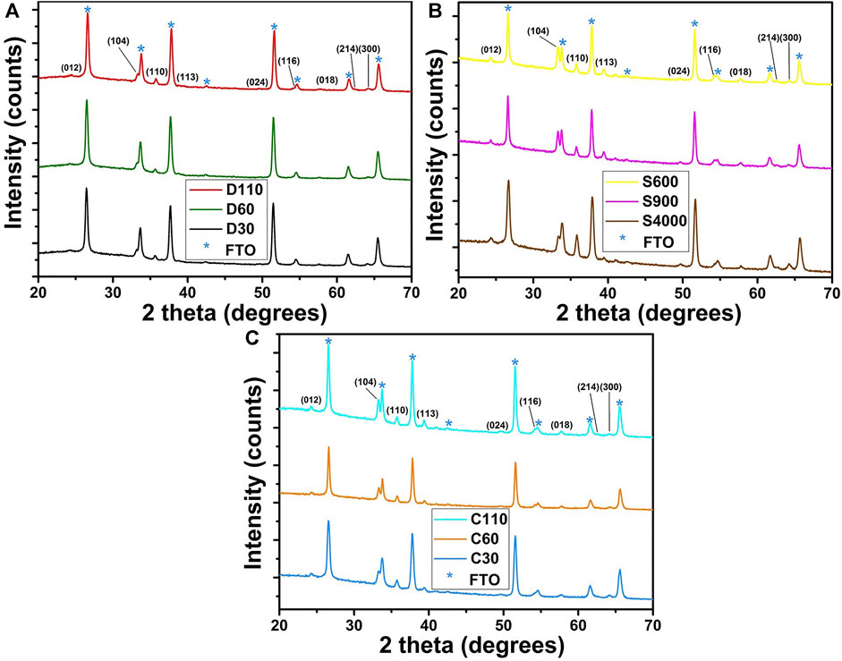
FIGURE 4. XRD pattern of α-Fe2O3 films prepared using the (A) dip (B) spin and (C) combined dip/spin coating techniques respectively.
The Debye-Scherrer approximation was used to estimate the crystal sizes of the α-Fe2O3 films using the (110) peaks of the films. Table 1 presents the full width at half maximum (FWHM) and crystal sizes estimated for the α-Fe2O3 films of various thicknesses prepared using different coating methods. The maximum crystal size value of 28.5 nm was obtained for the dip coated sample D60 while the least value of 21.8 nm was estimated for spin coated sample S4000. The films with 740–800 nm thickness range gave the maximum crystal size for each coating method used for samples preparation as shown in Figure 5. All dip coated films yielded higher crystal sizes while the ones produced via spin coating gave the least values across films of various thickness ranges (Figure 5). PEC water splitting can be promoted by improved crystallization due to the consequent reduction in electron scattering centers and improved conductivity associated with enhancement of crystal size (Aegerter et al., 1997; Schuler and Aegerter, 1999).
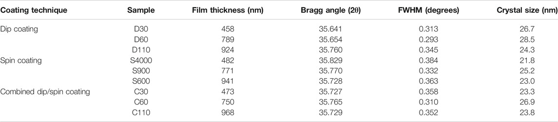
TABLE 1. The FWHM and crystal sizes estimated for the α-Fe2O3 films of various thicknesses prepared using different coating techniques.
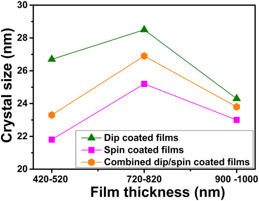
FIGURE 5. The crystal size of α-Fe2O3 films of various thickness ranges prepared using different coating techniques.
PEC Behavior
Photocurrent Response
LSV measurements were performed in dark and under light conditions on the α-Fe2O3 films prepared using the dip, spin and combined dip/spin coating methods to obtain their photoresponse and the results are shown in Figures 6A–C for the dip, spin and combined dip/spin coated films respectively. Films prepared using the dip coating method yielded the maximum photocurrent density of 34.6 μA/cm2 for sample D60 and values of 20.7 and 16.8 μA/cm2 was achieved for D30 and D110 at 1.23 V vs RHE respectively. All films prepared using the spin coating method yielded photocurrent density in the range of 6.8–7.8 μA/cm2 at 1.23 V vs RHE. The films prepared using the combined dip/spin coating method produced the maximum photocurrent density of 13.5 μA/cm2 for sample C60 with values of 10.7 and 9.7 μA/cm2 recorded for D30 and D110 at 1.23 V vs RHE respectively. Figure 6B presents the photocurrent density of the α-Fe2O3 films of different thicknesses for samples prepared using the various coating methods. All dip coated films yielded higher photoresponse at 1.23 V vs RHE compared to the films prepared using the spin and combined dip/spin coating methods across films of various thicknesses. Also, all the films prepared via the combined dip/spin coating method produced higher photocurrent values compared to spin coated films across films of all thickness range. The poor crystallization of spin coated films compared to others contributed to their low photoresponse. In addition, the preferential growth of spin coated films in the (104) plane may have resulted in low charge mobility and high recombination of electron-hole pairs contributing to the low photocurrent density attained by the films (Kment et al., 2015). Improved crystallization of dip coated films (Figure 5) can enhance electron mobility due to the resulting increment in the mean free path and the reduction of electrons scattering centers (Schuler and Aegerter, 1999) and. This is one reason why higher photocurrent densities were achieved for the dip coated films compared to others. Based on the samples prepared, films with thicknesses of 740–800 nm produced the best photocurrent density at 1.23 V vs RHE for all the coating methods used for sample preparation as shown in Figure 6D. However, spin coated films did not show any significant difference in their photoresponse across films of different thicknesses. Also, no saturation of photocurrent was observed for both spin and combined dip/spin coated films over the entire potential window suggesting poor charge separation efficiency and high electron/hole recombination rate at the film’s surface (Tahir and Wijayantha, 2010; Chen et al., 2014).
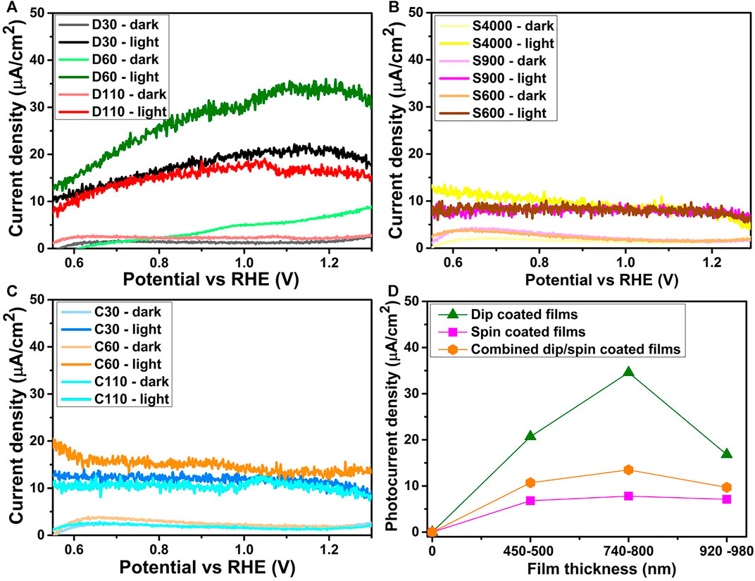
FIGURE 6. Current density of α-Fe2O3 films prepared using the (A) dip (B) spin and (C) combined dip/spin coating techniques respectively (D) shows the photocurrent density obtained at 1.23V vs RHE for films of various thickness ranges, prepared using different coating methods.
Electrochemical Impedance Spectroscopy (EIS) Analysis
Potentiostatic EIS measurements were conducted to study the effects of coating techniques on the charge transport mechanism in the bulk and on the surface of the α-Fe2O3 films. The Nyquist plots obtained from the EIS analysis are shown in Figures 7A,B for measurements done in dark and under illumination respectively while 6(c) presents the equivalent circuit model used to fit the raw EIS data. The circuit component Rs represents the series resistance associated with FTO/α-Fe2O3 contact, the electrolyte’s ionic conductivity and the external wire connections (Lopes et al., 2014). Rb and constant phase element 1 (CPE1) represents the charge transport resistance and the capacitance in the bulk of the α-Fe2O3 films respectively, assigned to the high frequency response associated with fast electronic processes (Lopes et al., 2014; Ahmed et al., 2018). Rct and CPE2 represent the charge transfer resistance at the α-Fe2O3/solution interface and the surface states capacitance respectively, associated with the low frequency response (Ahmed et al., 2018). CPE components were utilized to represent the non-ideal capacitive behaviours which may be due to the inhomogeneities of the films (Zhao et al., 2018). The results of fitting the raw EIS data to the modeled equivalent circuit using ZView software are presented in Table 2.
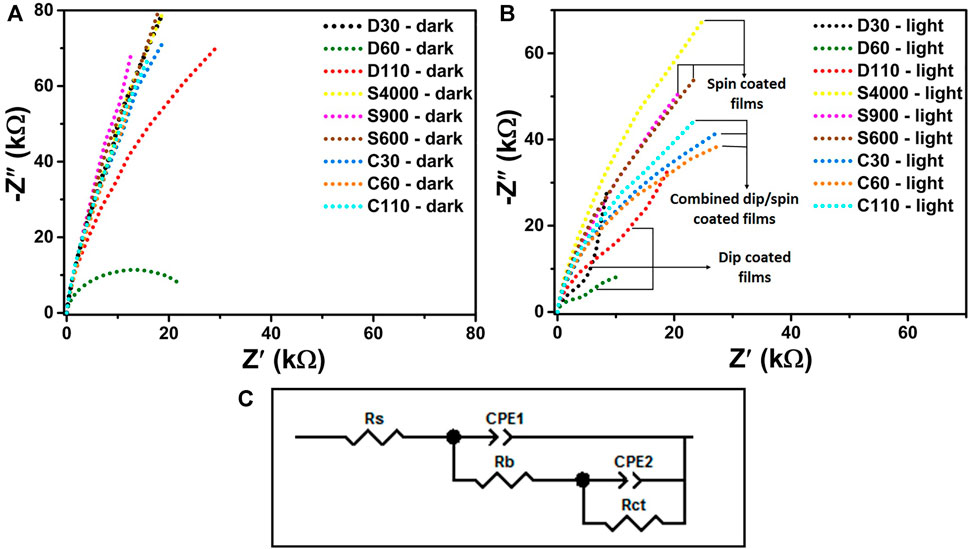
FIGURE 7. EIS analysis of α-Fe2O3 thin films for measurements performed under (A) dark and (B) illumination conditions respectively, and (C) shows the equivalent circuit model employed in fitting the raw EIS data.
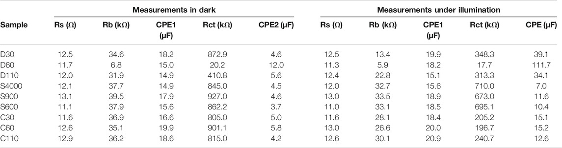
TABLE 2. Results of fitting raw EIS data to the equivalent circuit for α-Fe2O3 films prepared using different coating methods.
For measurements done under dark conditions (Figure 7A), the series resistance Rs for the films had values ranging between 11.1 and 13.1 Ω. The resistance to charge transport in the bulk of the films Rb, recorded the lowest value for dip coated sample D60 which was at least 4.7 times less than the values obtained for the other films. Low Rb can promote the movement of holes produce in the bulk of the films to the surface to perform water oxidation. The charge transfer resistance Rct, also yielded the least value of 20.6 kΩ for samples D60 followed by D110 with over 20 times higher Rct. All other films recorded high Rct values of over 39 times compared to the value recorded for D60. Lower Rct will allow for easier charge transfer at the α-Fe2O3/liquid interface which is important for efficient photocatalysis. The low Rb and Rct values recoded for D60 explained the high dark current at 1.23 V vs RHE observed for the films (Figure 6A) compared to the other samples.
For measurements done under light conditions given in Figure 7B, the Rs values for all the films approximately remained constant compared to the values obtained for the films under dark conditions, in line with the ohmic behaviour at the FTO/α-Fe2O3 interface (Klahr et al., 2012). Under illumination, the Rb and Rct values decrease for all the films in comparison to the values recorded in dark conditions which confirmed that all the samples prepared are photoactive. The charge transport resistance in the bulk of the photoanodes Rb yielded lower values for dip coated films with D60 producing the least value of 5.9 kΩ. The highest Rb values of 33.1 ± 0.4 kΩ were recorded for spin coated films. High Rb values will limit the movement of photogenerated holes from the bulk of the films to the surface to oxidize water. This contributed to the low photo response observe for spin coated films. Low Rct and high surface states capacitance (CPE2) which depicts the charge transfer kinetics taking place at the α-Fe2O3/liquid interface is always desired for the enhancement of photocatalysis. Rct values are generally higher compared to Rb values because water oxidation occurs at the α-Fe2O3/liquid interface which is often a major source of high resistance (Vardar et al., 2018).
Furthermore, because water oxidation occurs at the solid/liquid interface, a detailed analysis of the charge transfer resistance (Rct) and the surface states capacitance (CPE 2) of the films under illumination will be vital for a better understanding of the photoresponse of the films. Low Rct coupled with high surface states capacitance promotes photocatalysis by enhancing charge separation at the solid/liquid interface (Klahr et al., 2012; Xi and Lange, 2018). Figures 8A,B presents the Rct and CPE2 values for films of various thicknesses prepared using different coating methods respectively, for EIS measurements performed under light conditions. The highest Rct and least CPE2 values were recorded for spin coated films under illumination across samples of all thickness ranges, further accounting for the low photocurrent density values obtained for the films. This further explained the lack of photocurrent saturation observed for the films in the entire potential scan window as seen in Figure 6C. The high Rct values recorded for spin coated films is associated with crystal growth in the (104) plane, which has been linked with higher surface recombination due to the existence of non-ideal oxygen terminations on the films surface acting as charge trapping sites (Kment et al., 2015; Shinde et al., 2016). Samples prepared using the combined dip/spin coating method produce lower Rct and higher CPE2 values relative to spin coated films. This explained the improved photoresponse recorded for combined coated films over the spin coated ones. Dip coated samples D30 and D110 recorded higher Rct values compared to combined coated films, however, their Rb values (Table 1) were relatively lower. In addition, the surface state capacitance recorded for the films were more than double the values obtained for the combined dip/spin coated film. The lower bulk resistance and high surface state capacitance values for D30 and D110 resulted in the higher photocurrent densities obtained for the films compared to the dip/spin coated samples. Rct and CPE2 values of D30 and D110 are comparable, however, the bulk resistance to charge transport, Rb for D30 under light was 42% less than the value obtained for D110. This account for the slightly higher photocurrent density obtained for D30 compared to those of D110 films. For each coating method used for films preparation, the Rct and CPE2 recorded the least and highest values for samples with thickness in the range of 740–800 nm (D60, S900 and C60). Among these films, the dip coated sample D60 recorded the least and highest Rct and CPE2 values respectively. These explain the reason why films with 740–800 nm thickness produced the best photoresponse for each coating method used for samples preparation and justify the high photocurrent density achieved for D60.
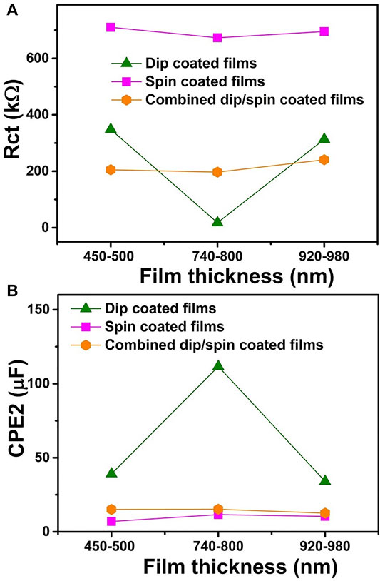
FIGURE 8. (A) the charge transfer resistance (Rct) and (B) the surface states capacitance (CPE2) for films of various thicknesses prepared using different coating methods respectively, for EIS measurements performed under light conditions.
Mott-Schottky (M-S) Studies
M-S analysis was performed to extract approximate values of the donor density (ND) and flat band potential (Vfb) of the α-Fe2O3 films. The ND and Vfb values were estimated for the films using the M-S relation in Eq. 4:
where C represent the capacitance of the space charge layer, A stands for the surface area of the electrode,
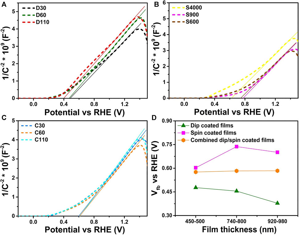
FIGURE 9. M-S plots of α-Fe2O3 films prepared using the (A) dip (B) spin and (C) combined dip/spin coating techniques respectively (D) shows the flat band potential values obtained for the films of various thickness ranges, prepared using different coating methods.
The slope (S) obtained from the linear fitting of the Mott-Schottky plots were used to estimate the donor densities of the α-Fe2O3 films using the expression
Table 3 gives the ND, and Vfb values estimated for the α-Fe2O3 films. The ND estimated for all the films yielded values ranging from (7.4–8.7) × 1019 cm−3 similar to the values reported for α-Fe2O3 in literature (Tamirat et al., 2016; Wickman et al., 2017). Coating techniques did not have a notable effect on the donor density of the films as the difference between the maximum and the least ND value is a magnitude of 1.3. However, coating techniques were found to have a noticeable effect on the Vfb values estimated for the films. Films prepared by dip coating technique had the most negative Vfb l values in the range of (0.37–0.47) V vs. RHE while spin coated films recorded the most positive values of (0.60–0.73) V vs. RHE. This observation was consistent across films of different thickness ranges prepared using the various coating methods as shown in Figure 9D. A more negative value for Vfb is indicative of better separation of charge carriers which is capable of improving photocatalysis (Vanags et al., 2015). Other properties such as the film thickness and other charge transport properties of the films can influence their photoelectrochemical behavior, as a result, a direct correlation between the Vfb and photocurrent density of the films was not observed.

TABLE 3. Mott-Schottky analysis data of films prepared using different coating techniques.
Conclusion
The PEC behaviour of α-Fe2O3 films prepared using dip, spin and combined dip-spin coating methods have been investigated. α-Fe2O3 films of 450–500, 740–800 and 920–980 ± 30 nm thicknesses were prepared using each of the coating methods to obtain a clear perspective on the influence of both film thickness and coating techniques on the PEC response of the films. Maximum photocurrent densities of 34.6, 7.8, and 13.5 μA/cm2 V vs RHE were obtained for dip, spin and combined dip/spin coated films with the thickness of 740–800 ± 30 nm respectively. Dip coated films produced the best photoresponse while the films prepared using the spin coating method yielded the least photocurrent values across films of different thicknesses. Improved crystallization, low charge transfer resistance at the solid/electrolyte junction, high surface states capacitance and more negative flat band potential values obtained for dip coated films are responsible for the enhanced photocurrent response recorded for the films. The low photocurrent obtained for spin coated films is largely attributed to the poor charge mobility and high surface recombination of electron-hole pairs due to their preferential crystal growth in the (104) plane. Based on the sample processing approaches employed in this research, the dip coating method is best suited for the preparation of α-Fe2O3 films for PEC water splitting. This research emphasized the importance of simultaneously optimizing both the coating techniques for film deposition and the film’s thickness in preparing α-Fe2O3 films for PEC applications.
Data Availability Statement
The original contributions presented in the study are included in the article/Supplementary Material, further inquiries can be directed to the corresponding author.
Author Contributions
PK: Conceptualization, methodology, investigation, formal analysis, visualization, validation, data curation, writing–original draft and writing–review and editing. NN: Methodology, investigation, supervision and writing–review and editing. MD: Methodology, data curation, validation, supervision, writing–review and editing and project administration.
Conflict of Interest
The authors declare that the research was conducted in the absence of any commercial or financial relationships that could be construed as a potential conflict of interest.
Acknowledgments
The authors acknowledge the National Research Foundation - The World Academy of Sciences (NRF-TWAS), grant UID; 110,814, the South African Research Chairs Initiative (SARCHI), UID; 115,463 and the University of Pretoria for financial support. We acknowledge financial support from NRF N00500, project UID; 110,983 (Blue Skies Research Program), UID; 112,085 (NRF Research Development Grant), and the CSIR National Laser Center Rental Pool Program toward the purchase of VersaStat 3 F potentiostat.
Supplementary Material
The Supplementary Material for this article can be found online at: https://www.frontiersin.org/articles/10.3389/fenrg.2021.683293/full#supplementary-material
References
Aegerter, M. A., Reich, A., Ganz, D., Gasparro, G., Pütz, J., and Krajewski, T. (1997). Comparative Study of SnO2:Sb Transparent Conducting Films Produced by Various Coating and Heat Treatment Techniques. J. non-crystalline Sol. 218, 123–128. doi:10.1016/s0022-3093(97)00134-8
Ahmed, A. Y., Ahmed, M. G., and Kandiel, T. A. (2018). Hematite Photoanodes with Size-Controlled Nanoparticles for Enhanced Photoelectrochemical Water Oxidation. Appl. Catal. B: Environ. 236, 117–124. doi:10.1016/j.apcatb.2018.04.073
Ahn, H.-J., Kwak, M.-J., Lee, J.-S., Yoon, K.-Y., and Jang, J.-H. (2014). Nanoporous Hematite Structures to Overcome Short Diffusion Lengths in Water Splitting. J. Mater. Chem. A. 2, 19999–20003. doi:10.1039/c4ta04890c
Bora, D. K., Braun, A., Erat, S., Ariffin, A. K., Löhnert, R., Sivula, K., et al. (2011). Evolution of an Oxygen Near-Edge X-Ray Absorption Fine Structure Transition in the Upper Hubbard Band in α-Fe2O3 upon Electrochemical Oxidation. J. Phys. Chem. C 115, 5619–5625. doi:10.1021/jp108230r
Chen, H., Wei, Z., Yan, K., Bai, Y., Zhu, Z., Zhang, T., et al. (2014). Epitaxial Growth of ZnO Nanodisks with Large Exposed Polar Facets on Nanowire Arrays for Promoting Photoelectrochemical Water Splitting. Small 10, 4760–4769. doi:10.1002/smll.201401298
Deepa, M., Saxena, T. K., Singh, D. P., Sood, K. N., and Agnihotry, S. A. (2006). Spin Coated versus Dip Coated Electrochromic Tungsten Oxide Films: Structure, Morphology, Optical and Electrochemical Properties. Electrochimica Acta 51, 1974–1989. doi:10.1016/j.electacta.2005.06.027
Dias, P., Vilanova, A., Lopes, T., Andrade, L., and Mendes, A. (2016). Extremely Stable Bare Hematite Photoanode for Solar Water Splitting. Nano Energ. 23, 70–79. doi:10.1016/j.nanoen.2016.03.008
Feng, F., Li, C., Jian, J., Li, F., Xu, Y., Wang, H., et al. (2020). Gradient Ti-Doping in Hematite Photoanodes for Enhanced Photoelectrochemical Performance. J. Power Sourc. 449, 227473. doi:10.1016/j.jpowsour.2019.227473
GonçAlves, R. H., Lima, B. H., and Leite, E. R. (2011). Magnetite Colloidal Nanocrystals: A Facile Pathway to Prepare Mesoporous Hematite Thin Films for Photoelectrochemical Water Splitting. J. Am. Chem. Soc. 133, 6012–6019. doi:10.1021/ja111454f
Hjiri, M. (2020). Highly Sensitive NO2 Gas Sensor Based on Hematite Nanoparticles Synthesized by Sol-Gel Technique. J. Mater. Sci. Mater. Electron. 31, 5025–5031. doi:10.1007/s10854-020-03069-4
Jalli, J., Hong, Y.-K., Lee, J.-J., Abo, G. S., Park, J.-H., Lane, A. M., et al. (2010). Conversion of Worm-Shaped Antiferromagnetic Hematite to Ferrimagnetic Spherical Barium-Ferrite Nanoparticles for Particulate Recording Media. IEEE Magn. Lett. 1, 4500204. doi:10.1109/lmag.2010.2087315
Kant, R., Pathak, S., and Dutta, V. (2018). Design and Fabrication of Sandwich-Structured α-Fe2O3/Au/ZnO Photoanode for Photoelectrochemical Water Splitting. Solar Energ. Mater. Solar Cell 178, 38–45. doi:10.1016/j.solmat.2018.01.005
Khakpour, Z., Pourfarahani, H., Maghsoudipour, A., and Ebadzadeh, T. (2018). Synthesis and Deposition of Hematite Nanoparticles on Fluorine-Doped Tin Oxide (FTO) Glass Substrates. Mater. Today Proc. 5, 15828–15835. doi:10.1016/j.matpr.2018.05.081
Kim, J. Y., Magesh, G., Youn, D. H., Jang, J.-W., Kubota, J., Domen, K., et al. (2013). Single-crystalline, Wormlike Hematite Photoanodes for Efficient Solar Water Splitting. Scientific Rep. 3, 2681. doi:10.1038/srep02681
Klahr, B., Gimenez, S., Fabregat-Santiago, F., Hamann, T., and Bisquert, J. (2012). Water Oxidation at Hematite Photoelectrodes: the Role of Surface States. J. Am. Chem. Soc. 134, 4294–4302. doi:10.1021/ja210755h
Kment, S., Schmuki, P., Hubicka, Z., Machala, L., Kirchgeorg, R., Liu, N., et al. (2015). Photoanodes with Fully Controllable Texture: the Enhanced Water Splitting Efficiency of Thin Hematite Films Exhibiting Solely (110) Crystal Orientation. ACS nano 9, 7113–7123. doi:10.1021/acsnano.5b01740
Kyesmen, P. I., Nombona, N., and Diale, M. (2019). Influence of Coating Techniques on the Optical and Structural Properties of Hematite Thin Films. Surf. Inter. 17, 100384. doi:10.1016/j.surfin.2019.100384
Landau, L., and Levich, B. (1942). Dragging of a Liquid by a Moving Plate. (Moscow: ActaPhysicochimica. URSS).
Lee, K.-R., Hsu, Y.-P., Chang, J.-K., Lee, S.-W., Tseng, C.-J., and Jang, J. S.-C. (2014). Effects of Spin Speed on the Photoelectrochemical Properties of Fe2O3 Thin Films. Int. J. Electrochem. Sci. 9, 7680–7692.
Liang, Y., Enache, C. S., and Van De Krol, R. (2008). Photoelectrochemical Characterization of Sprayed. Int. J. Photoenergy 2008. doi:10.1115/ijtc2008-71057
Lopes, T., Andrade, L., Le Formal, F., Gratzel, M., Sivula, K., and Mendes, A. (2014). Hematite Photoelectrodes for Water Splitting: Evaluation of the Role of Film Thickness by Impedance Spectroscopy. Phys. Chem. Chem. Phys. 16, 16515–16523. doi:10.1039/c3cp55473b
Naz, S., Islam, M., Tabassum, S., Fernandes, N. F., Carcache de Blanco, E. J., and Zia, M. (2019). Green Synthesis of Hematite (α-Fe2O3) Nanoparticles Using Rhus Punjabensis Extract and Their Biomedical Prospect in Pathogenic Diseases and Cancer. J. Mol. Struct. 1185, 1–7. doi:10.1016/j.molstruc.2019.02.088
Puetz, J., and Aegerter, M. A. (2004). “Dip Coating Technique,” in Sol-Gel Technologies for Glass Producers and Users. Editors M. A. Aegerter, and M. Mennig (Boston: Springer), 37–48. doi:10.1007/978-0-387-88953-5_3
Quiterio, P., Apolinário, A., Navas, D., Magalhaes, S., Alves, E., Mendes, A. M., et al. (2020). Photoelectrochemical Water Splitting: Thermal Annealing Challenges on Hematite Nanowires. The J. Phys. Chem. C 124, 12897–12911. doi:10.1021/acs.jpcc.0c01259
Rajendran, K., Karunagaran, V., Mahanty, B., and Sen, S. (2015). Biosynthesis of Hematite Nanoparticles and its Cytotoxic Effect on HepG2 Cancer Cells. Int. J. Biol. Macromolecules 74, 376–381. doi:10.1016/j.ijbiomac.2014.12.028
Reddy, C. V., Reddy, I. N., Akkinepally, B., Reddy, K. R., and Shim, J. (2020). Synthesis and Photoelectrochemical Water Oxidation of (Y, Cu) Codoped α-Fe2O3 Nanostructure Photoanode. J. Alloys Comp. 814, 152349. doi:10.1016/j.jallcom.2019.152349
Schuler, T., and Aegerter, M. A. (1999). Optical, Electrical and Structural Properties of Sol Gel ZnO:Al Coatings. Thin Solid Films 351, 125–131. doi:10.1016/s0040-6090(99)00211-4
Shinde, P. S., Choi, S. H., Kim, Y., Ryu, J., and Jang, J. S. (2016). Onset Potential Behavior in α-Fe2O3 photoanodes: the Influence of Surface and Diffusion Sn Doping on the Surface States. Phys. Chem. Chem. Phys. 18, 2495–2509. doi:10.1039/c5cp06669g
Sivula, K., Le Formal, F., and Le Formal, M. (2011). Solar Water Splitting: Progress Using Hematite (α-Fe2O3) Photoelectrodes. ChemSusChem 4, 432–449. doi:10.1002/cssc.201000416
Sivula, K., Zboril, R., Le Formal, F., Robert, R., Weidenkaff, A., Tucek, J., et al. (2010). Photoelectrochemical Water Splitting with Mesoporous Hematite Prepared by a Solution-Based Colloidal Approach. J. Am. Chem. Soc. 132, 7436–7444. doi:10.1021/ja101564f
Souza, F. L., Lopes, K. P., Nascente, P. A. P., and Leite, E. R. (2009). Nanostructured Hematite Thin Films Produced by Spin-Coating Deposition Solution: Application in Water Splitting. Solar Energ. Mater. solar Cell 93, 362–368. doi:10.1016/j.solmat.2008.11.049
Tahir, A. A., and Wijayantha, K. G. U. (2010). Photoelectrochemical Water Splitting at Nanostructured ZnFe2O4 Electrodes. J. Photochem. Photobiol. A: Chem. 216, 119–125. doi:10.1016/j.jphotochem.2010.07.032
Tamirat, A. G., Dubale, A. A., Su, W.-N., Chen, H.-M., and Hwang, B.-J. (2017). Sequentially Surface Modified Hematite Enables Lower Applied Bias Photoelectrochemical Water Splitting. Phys. Chem. Chem. Phys. 19, 20881–20890. doi:10.1039/c7cp02890c
Tamirat, A. G., Rick, J., Dubale, A. A., Su, W.-N., and Hwang, B.-J. (2016). Using Hematite for Photoelectrochemical Water Splitting: a Review of Current Progress and Challenges. Nanoscale Horiz. 1, 243–267. doi:10.1039/c5nh00098j
Tyona, M. D. (2013). A Comprehensive Study of Spin Coating as a Thin Film Deposition Technique and Spin Coating Equipment. Adv. Mater. Res. 2, 181–193. doi:10.12989/amr.2013.2.4.181
Vanags, M., Šutka, A., Kleperis, J., and Shipkovs, P. (2015). Comparison of the Electrochemical Properties of Hematite Thin Films Prepared by Spray Pyrolysis and Electrodeposition. Ceramics Int. 41, 9024–9029. doi:10.1016/j.ceramint.2015.03.272
Vardar, G., Bowman, W. J., Lu, Q., Wang, J., Chater, R. J., Aguadero, A., et al. (2018). Structure, Chemistry, and Charge Transfer Resistance of the Interface between Li7La3Zr2O12 Electrolyte and LiCoO2 Cathode. Chem. Mater. 30, 6259–6276. doi:10.1021/acs.chemmater.8b01713
Wang, H., and Turner, J. A. (2010). Characterization of Hematite Thin Films for Photoelectrochemical Water Splitting in a Dual Photoelectrode Device. J. Electrochem. Soc. 157, F173–F178. doi:10.1149/1.3489940
Wickman, B., Fanta, A. B., Burrows, A., Hellman, A., Wagner, J. B., and Iandolo, B. (2017). Iron Oxide Films Prepared by Rapid Thermal Processing for Solar Energy Conversion. Scientific Rep. 7, 40500. doi:10.1038/srep40500
Xi, L., and Lange, K. (2018). Surface Modification of Hematite Photoanodes for Improvement of Photoelectrochemical Performance. Catalysts 8, 497. doi:10.3390/catal8110497
Keywords: α-Fe2O3, dip coating, spin coating, combined dip/spin coating, PEC behaviour
Citation: Kyesmen PI, Nombona N and Diale M (2021) Effects of Film Thickness and Coating Techniques on the Photoelectrochemical Behaviour of Hematite Thin Films. Front. Energy Res. 9:683293. doi: 10.3389/fenrg.2021.683293
Received: 20 March 2021; Accepted: 27 April 2021;
Published: 10 May 2021.
Edited by:
Hadi Rostamzadeh, Sharif University of Technology, IranReviewed by:
Amin Yourdkhani, Tarbiat Modares University, IranYiming Tang, South China Normal University, China
Copyright © 2021 Kyesmen, Nombona and Diale. This is an open-access article distributed under the terms of the Creative Commons Attribution License (CC BY). The use, distribution or reproduction in other forums is permitted, provided the original author(s) and the copyright owner(s) are credited and that the original publication in this journal is cited, in accordance with accepted academic practice. No use, distribution or reproduction is permitted which does not comply with these terms.
*Correspondence: Mmantsae Diale, mmantsae.diale@up.ac.za