High-precision bus voltage control based on NLESO and TSMC predicted load current and grid voltage differential feedforward
 Di Xie
 Liangliang Wang
 Zhi Zhang
 Shoumo Wang2
 - 1New Energy Research Center, School of Electric Power, South China University of Technology, Guangzhou, China
- 2Guangdong HYNN Technologies Co., Ltd, Dongguan, China
- 3Department of Electrical Engineering and Automation, Dongguan University of Technology, Dongguan, China
Power battery test equipment is widely used to produce and test new energy vehicles and storage containers. To address the problem of DC bus voltage fluctuations that affect the accuracy of output voltage and current, a high-accuracy bus voltage control strategy is based on nonlinear extended state observation (NLESO) and terminal silding mode controller (TSMC) load current estimation. Simulation and experimental results show that the control strategy has a good suppression effect on the DC bus voltage fluctuation and can effectively improve the accuracy of the DC side output voltage and current. Grid voltage differential feedforward is adopted, which can achieve fast suppression of DC bus voltage fluctuations in power battery test equipment and meet the high precision output requirements of the system DC bus.
1 Introduction
In response to China’s “2030 Carbon Peak” policy, new energy technologies have been developed rapidly. Electrochemical energy storage technology has become mainstream, covering the three major energy consumption fields of transportation, industry, and buildings, and has been widely applied in electric vehicles and energy storage and power generation systems (Wang et al., 2014; Ali et al., 2021). However, with the expansion of market capacity, the safety of power batteries and energy storage containers is being widely considered. The production, operation, and maintenance of power battery packs must go through perfect high-precision performance testing to ensure system safety and reliability. Therefore, the power battery testing system has been developed rapidly. The main components of the power battery testing system are high-precision and high-power energy storage and power battery professional testing equipment, which can simulate energy storage power stations, electric vehicles, and other operating conditions. Combined with international and domestic testing standards, a comprehensive test of the electrical performance parameters for power batteries can be carried out to obtain complete and accurate data for a comprehensive assessment of battery quality, which provides a scientific basis for the research, production, and application of energy storage and power batteries.
High-precision power battery testing equipment is mainly used for electric vehicle packs, energy storage container packs, and DC charge and discharge operation condition testing of energy storage containers. Tests include battery pack condition-simulation tests, charge and discharge characteristics tests of the battery pack, battery pack capacity tests, battery cycle life tests, and BMS performance verification tests. The controlled object during the test involves the test equipment’s input and output characteristic parameters. Test equipment must be equipped with high-precision detection and control, high-quality power feedback, high-standard operation condition simulation tests, a wide range of DC voltages and sizeable current output performance (Huang et al., 2016; Zhang and Ruan, 2019; Zhou et al., 2019; Ma et al., 2019; Cao et al., 2018; Zhou et al., 2015).
Figure 1 shows 1600 V high-power, high-precision power battery test equipment with a two-level topology. An NPC-type three-level topology is adopted in the AC/DC module, a two-level topology is adopted in the DC/DC module, and a DC bus capacitor connects the multiple DC modules (Aksenov et al., 2016; Leal, 2017; Zhao et al., 2017; Wu et al., 2019). The control accuracy is less than 0.1% under the condition of high voltage and large current on the DC side. A dynamic DC output response time of less than 20 ms is required at an instantaneous full load. Some conditions include sudden changes in DC side load, output power, and AC/DC power disturbances. This will cause a significant impact on the bus voltage, making the DC bus voltage unable to operate within the set range, which in turn affects the measurement accuracy of voltage and current on the DC output side. This can seriously affect the entire simulation process, resulting in the severe distortion of test data (Jamma et al., 2017; Geng et al., 2018). Therefore, the stable control of the DC bus voltage plays a significant role in the high accuracy characteristics of the DC side of the test equipment. The bus voltage control must have a high level of immunity to interference to improve the output accuracy on the DC side.
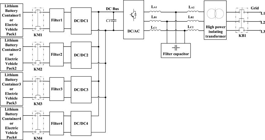
FIGURE 1. Two-stage topology with multiple DC modules for test equipment.
At present, the system accuracy is optimized by improving the control strategy of the bidirectional AC/DC converter and the suppression of disturbance voltage fluctuations and harmonics. The traditional control strategy uses proportional integration (PI) double-loop control, which cannot wholly solve the changes and shocks of the bus voltage at instantaneous full load, nor can it effectively suppress the disturbing harmonics on the grid side. For this reason, many scholars have proposed a dual closed-loop control strategy that adds feedforward and observers to improve the response rate of tracking external disturbances by varying the feedforward value of the current inner loop (Li et al., 2018; Hui et al., 2019; Wang et al., 2020). To some extent, power feedforward and current feedforward control can improve the bus voltage fluctuation response. Nevertheless, since the feedforward is obtained from the current inner loop regulation, the output can lag behind the given value of the current. Adding a DC bus current transformer to collect real-time information can solve the feedforward control problem when the busload changes (Baazoug et al., 2018; Isik et al., 2018). This adds extra cost and makes selecting high-current DC transformers more difficult. A nonlinear disturbance observer is chosen to make virtual measurements of the load current and synchronize the bus voltage control to solve this problem. At the same time, other grid voltage second-order differential feedforward loops are needed to address the DC bus power fluctuations introduced by the grid’s harmful sequence components and suppress the high-frequency oscillation-type changes in the DC bus voltage caused by uncertain grid distortions (Xiong and Ye, 2019).
The expansion state observer in the nonlinear perturbation observer enables accurate estimation of each of the nonlinear state variables in the system. An accurate real-time estimate of the system state variables without building a mathematical system model makes it difficult to quantify the gain in control quantities (Changchao and Zhongjian, 2020; Fu et al., 2022). The state observer and the TSMC combination can realize the system state variables to converge quickly in a finite time. The problem of asymptotic convergence of common sliding mode control is solved. This has the property of jitter elimination without switching terms (Liang et al., 2019; Ding et al., 2020; Henao-Bravo et al., 2020).
This paper optimizes the control strategy of a bidirectional AC/DC converter for medium-voltage high-precision power battery test equipment by an expansive state observer and grid voltage second-order differential feedforward control. Based on the traditional double closed-loop control strategy, a load current and grid voltage second-order differential feedforward control are added to avoid increasing hardware costs and to provide real-time tracking of external disturbances and grid uncertainties. Bus voltage fluctuations in the test system are quickly suppressed, and the DC high-precision output requirement of the system is met. This paper verifies that the controller optimized with this control strategy can stop DC bus voltage fluctuations, improve the dynamic response characteristics, ensure the operational stability of the two-stage system and effectively improve the output accuracy of the DC side. Simulations and platform tests were implemented with 1600 V 800 kW power battery test equipment.
The rest of the paper is organized as follows. The influence of grid voltage imbalance and its harmonic components on bus voltage fluctuations are derived and analysed in Section 2. The effect of load current and grid voltage disturbances on bus voltage control through closed-loop transfer functions is investigated and gives the corresponding feedforward control expressions in Section 3. Section 4 presents the load current observation method based on nonlinear expansion state observation and terminal sliding mode control. Section 5 offers a simulation comparison between the proposed control strategy and the conventional PI double closed-loop control strategy under different charging and discharging conditions. An experimental certification analysis of the control effect of the control strategy proposed in this paper on high-power energy storage test equipment is described in Section 6. The conclusions are provided in Section 7.
2 Disturbance analysis of grid voltage
The equipment circuit topology is shown in Figure 2. The buck/boost topology is adopted in the DC-DC converter, and the neutral point clamped three-level topology is adopted in the AC-DC converter. ex and ux represent the three-phase inverter voltages and three-phase grid voltages on the AC side of the converter, respectively, where x is equal to a, b, and c. L1, L2, and C1 indicate the inductors and capacitors of the LCL filter on the AC side. L3, L, and C2 denote inductors and capacitors of the LCL filter on the DC side. iinv and ig represent the inverter current and grid current, respectively. C, Vdc, Vbat, and ibat indicate the filter capacitor, bus voltage, output voltage, and current, respectively. ii, io, and ic represent the input current, output current, and capacitor current, respectively.
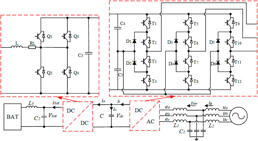
FIGURE 2. Equipment circuit topology.
When distortions occur in the grid after an imbalance, in addition to the fundamental component, there are harmful sequence components and corresponding harmonic components in the grid voltage. The harmonic part is most commonly found in the 5th and 7th order. The presence of harmonic components in the traditional Dq control algorithm will cause fluctuations in power on the DC side, which will lead to changes in the bus voltage and affect the accuracy of the control of the battery voltage and current at the output of the device.
In the case of grid imbalance, the grid voltage and current vectors can be decomposed into the sum of the positive sequence components and the corresponding harmful sequence components, as shown in (1).
where
According to the theory of AC instantaneous power calculation, the expression for the transmitted power under grid unbalance can be obtained as
The superscript "∗" in (2) indicates the conjugate complex, and the active power P and reactive power Q can be expressed as
In (3), P0 and Q0 are the DC components of active and reactive power, and Pc2, Ps2, Qc2, and Qs2 are the amplitude of active and reactive power two times the frequency fluctuation.
When the grid contains the 5th and 7th harmonics, the active power transmitted by the AC/DC converter can be obtained by the same analysis.
In (4), Pc6, Ps6, Qc6, and Qs6 are the amplitudes of the 6 times frequency pulsation of active and reactive power, Pc12, Ps12, Qc12, and Qs12 are the amplitudes of the 12 times frequency pulsation of active and reactive power.
The power loss on the AC and DC sides of the test equipment is ignored. Energy conservation for AC and DC power transfer is given when there is a grid voltage imbalance or a significant harmonic content.t
In (5), Pcn and Psn indicate the n times frequency active power pulsation amplitude. As seen from (5), the charge and discharge currents of the electrical test equipment remain constant. Fluctuations in the DC bus voltage are caused when the grid voltage is unbalanced or contains harmonic components.
To analyse the impact of bus voltage fluctuations on the accuracy of the voltage and current control on the device’s output side, the converter circuit topology of the DC-DC side is analysed by a mathematical model. The equation of state of the bidirectional buck/boost converter can be expressed as
where d1 and d2 denote the turn-on duty cycle of switch tubes Q1 and Q2, respectively.
Linearize the small signal of (6).
Udc, Ubat, IL, Io, and Ii represent the steady-state values of Vdc, Vbat, iL, io, and ii, respectively. Vdc, △Vbat, △iL, △io, and △ii denote the small signal disturbance values of the corresponding variables.
Substitute (7) into (6). The small-signal model of the linearized bidirectional DC/DC converter can be obtained.
From (8), it can be seen that unbalanced input and output currents on the bus capacitor cause bus voltage fluctuations. The fluctuations in bus voltage will further lead to changes in voltage and current on the output side, which affects the accuracy of charging and discharging voltage and current control of the equipment. To solve the influence of grid voltage and load–current disturbance on the bus voltage control accuracy and improve the equipment charging and discharging voltage and current control accuracy, this paper proposes a voltage and current feedforward control method based on grid voltage differential feedforward and ESO load current feedforward estimation.
3 Feedforward principle of voltage and current
The AC/DC converter of equipment supports bidirectional energy flow. The current inner loop uses AC feedback ig to improve the quality of the grid-connected current. The dual closed-loop control block diagram of the LCL-type AC/DC converter is shown in Figure 3(Wang et al., 2014).
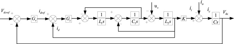
FIGURE 3. Block diagram of the double closed-loop control of the LCL converter.
According to the conservation of power on the AC side and the DC side, (9) is given.
Ud and id are the d-axis components of the grid voltage and grid current in the DQ transform. idc = ic.
From (9), the relation between the active component of the inverter current and the DC can be obtained.
where
The dual closed-loop control block diagram for the AC/DC converter shown in Figure 3 is simplified by moving the node equivalents.
The output bus voltage of the AC/DC converter can be obtained from Figure 4.
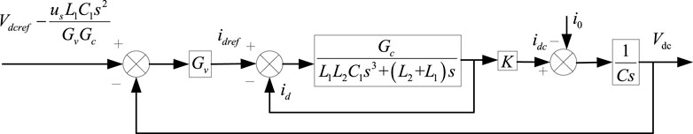
FIGURE 4. Simplified dual closed-loop control block diagram of the LCL converter.
Gref, Gu and Gi represent the bus command voltage’s closed-loop transfer function, the grid voltage disturbance’s closed-loop transfer function, and the load current disturbance’s closed-loop transfer function. Vdcref is the command value of bus voltage, and Gv and Gc are voltage loop and current loop controller transfer functions, respectively.
It can be seen from (11) that the bus voltage fluctuation is affected by the bus voltage command change and is related to the grid voltage disturbance and DC load current disruption. The bus voltage fluctuations are suppressed by adding feedforward control to eliminate the effect of grid voltage and load–current disturbances on the bus voltage.
The block diagram of the dual closed-loop control of an AC/DC converter with the addition of feedforward control can be expressed as follows.
The dual closed-loop control block diagram for the LCL converter shown in Figure 5 with the addition of feedforward control is simplified by moving the nodes equivalently.
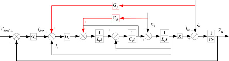
FIGURE 5. Block diagram of double closed-loop control with the addition of feed-forward control.
The output bus voltage of the AC/DC converter after the addition of feedforward control can be obtained from Figure 6.
where
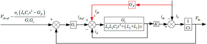
FIGURE 6. Simplified double closed-loop control block diagram with the addition of feedforward control.
To eliminate the influence of load current and grid voltage disturbance on bus control accuracy. The voltage–current feedforward control transfer function can be obtained from (14).
Based on the equipment parameter information provided in the article and Eqs 11–14, the open-loop Bode diagrams of the bus voltage loop before and after the addition of grid voltage and load current feedforward control can be plotted.
Figure 7 shows that the system margin of magnitude and phase margin are greatly improved, and the system is more stable after adding grid voltage and load current feedforward control.
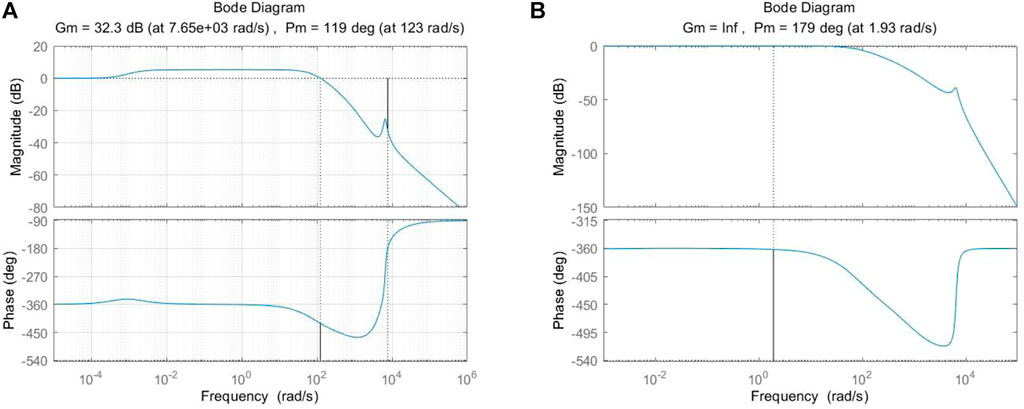
FIGURE 7. (A, B) shows the system margin of magnitude andphase margininthe traditional double closed-loop control strategy and the control strategy proposed in this paper, respectively.
Based on the above theoretical analysis, this paper proposes a control strategy of grid voltage differential and output current double feedforward. The output current is predicted by a method based on NLESO and TMSC. The system central circuit topology and loop control block diagram are shown in Figure 8.
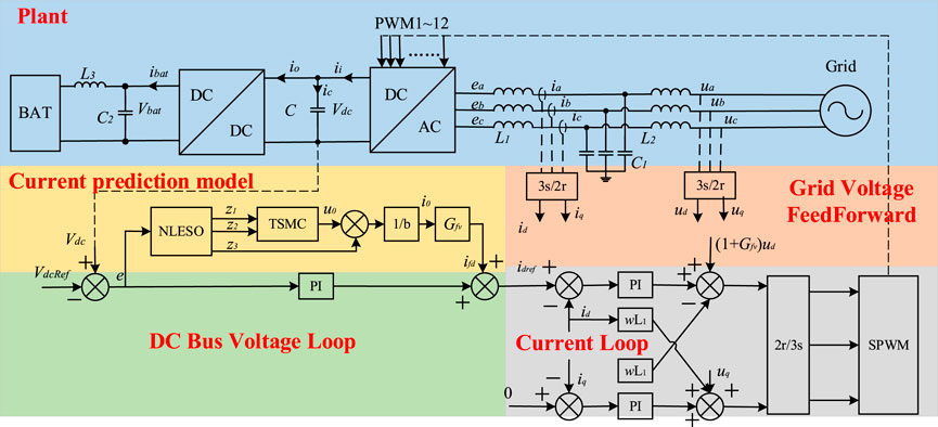
FIGURE 8. System primary circuit topology and loop control block diagram.
4 Estimation of load current disturbance
4.1 Design of a nonlinear expansion state observer
Multiple DC-DC charging and discharging control channels are usually for high-precision battery charging and canning equipment. In the above current feedforward control method, the AC/DC side requires simultaneous sampling of multiple channels of real-time battery current data, increasing the system’s cost and significantly impacting the system’s reliability. An expansion state observer and terminal-sliding-mode control techniques are used to solve the above problems to achieve a real-time estimation of load current and feedforward control.
On the DC side of the AC/DC converter, Kirchhoff’s current law is given by (16).
PI controls the current inner loop, and the transfer function Gc of the current loop controller is shown in (17).
Combining (15) and (17), and according to the load current feedforward control block diagram, the feedforward current value can be calculated as shown in (18).
The Laplace inverse transformation of (18) is given by (19).
Combined with (19) and the derivation of (16), (20) is derived as
(20)can be expressed in the form of the equation of state.
Combining Equations (20) and (21), the corresponding system state variable x1 in the state equation, the system external disturbance signal w(t), the system control quantity gain coefficient b, and the system control action quantity u(t) are obtained as shown in (22).
The system shown in (21) is a second-order system, so only a third-order expansion state observer needs to be designed to estimate the states x1 and x2 and the system’s uncertainty factor w(t). The third-order expansion state observer is designed as
In (23), β1, β2, and β3 indicate the observer gains, which can be determined by the zero-pole configuration method. z1, z2, and z3 denote the outputs of the expansion state observer.
where δ denotes the interval length of the linear segment near the origin and δ > 0, α is the amplification factor, and 0 < α < 1.δxi = zi-xi, where i = 1,2,3, (25) is obtained from the difference between (23) and (21).
Since the nonlinear function g(e1) is smooth and g(0) = 0, according to Taylor’s formula, (25) can be rewritten as
Assuming
where
If the system is to remain stable under the effect of unknown disturbances and reach a sound balance quickly, the eigenvalues of compensation matrix A must fall in the left half-plane of the complex plane. According to the zero-pole configuration method, the desired pole pi(i = 1,2,3) is selected such that the parameter li(i = 1,2,3) in the parameter compensation matrix A satisfies (28).
According to (28), the values of parameters l1, l2, and l3 can be found, and the system expansion state observer shown in (23) can be rewritten as
4.2 Design of sliding mode controllers
Assuming the system is a single-input and single-output nonlinear system, the mathematical model of the system is shown in (30).
where xi, f(x), g(x), and u(x) denote the state variables of the system, the nonlinear function, the nonlinear function associated with the system error, and the amount of control action of the system, respectively.
For any n-order system, a global fast sliding mode with a recursive structure [25] can be chosen, as expressed in (31).
where αi, βi>0 and pi, qi (pi > qi) (i = 0,1...,n-2) are positive odd numbers. S means slip surface.
From (31), where i = 1,2...,n-1, the n-order differential of si can be expressed as
A recursive calculation based on (30) can be expressed as
Assuming that the trace instruction value is r,
(35) is obtained by substituting Eqs 34, 30 into Eq. 33:
Taking the global fast sliding mode control law as
(37) can be derived by (36) and 35.
Defining the Lyapunov function as
From (38), it can be seen that V is less than 0. According to Lyapunov stability theory, the sliding mode control system is stable, and sliding mode sn-1 will converge to zero in a finite time.
It can be seen that the system in this paper is a second-order system by (21), and according to the above global sliding-mode-controller design principle, the sliding mode surface is selected, as shown in (39).
The fast terminal sliding mode is constructed as
where p0 and q0 are both positive odd numbers. If 1 < p0/q0 < 2 is satisfied, α and β are positive values, and by combining (29), (39), and (40), (41) is given.
The values of u0 and c1 are taken as follows:
The final control law of the load current feedforward value is obtained, as shown in (43), by substituting Eq. 42 into Eq. 41.
5 Analysis of system simulation
5.1 Simulation model
To observe the stability of DC bus voltage control of medium-voltage high-power high-precision power battery test equipment based on an expansion state observer and second-order differential feedforward grid voltage control, a simulation model of the power battery test system is established for analysis.
A 1600 V 800 kW power battery test system is shown in Figure 9. The model contains the grid, AC/DC converter, DC/DC converter, power battery pack of electric vehicles, AC output isolation transformer, and AC load. The load power battery pack module parameters are shown in Table 1. The DC/DC converter is connected to the AC/DC converter by a bus capacitor. The DC output voltage of the DC/DC converter can be controlled from 50 to 1600 V. The DC voltage range at the AC/DC and bus capacitor connection is from 1300 to 1650 V. A rated power of 850 kW could be obtained for the AC-DC converter, which meets the rated efficiency losses.
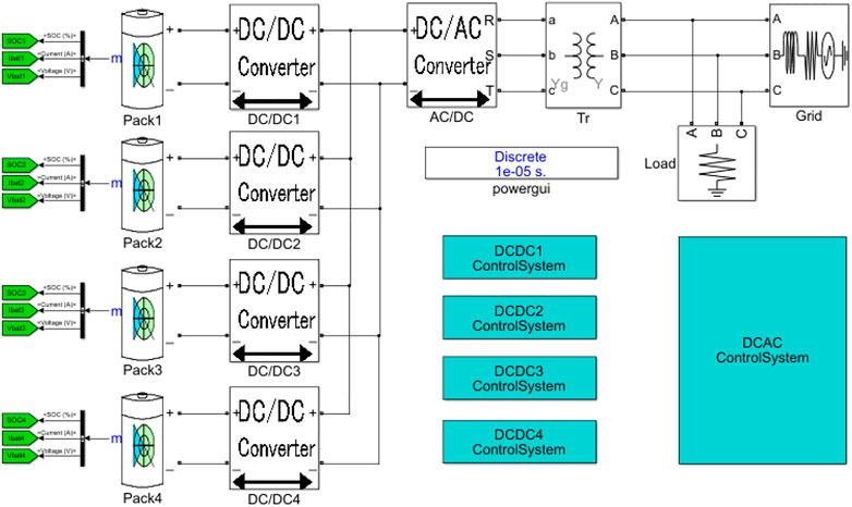
FIGURE 9. Model of the power battery test system.
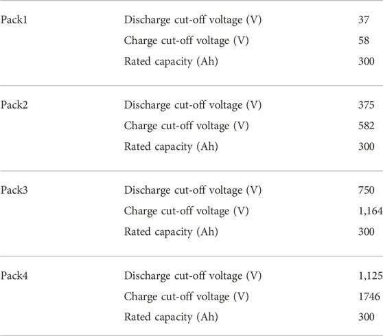
TABLE 1. Parameters for each Pack module of the system.
The parameters of each Pack module in the simulation model are shown in Table 1.
A conventional two-loop control strategy and a second-order differential feedforward control strategy based on an expansive state observer and grid voltage are applied in the simulation model of the AC/DC converter. The controller parameters used in the simulation model are shown in Table 2, the parameters l1, l2, and l3 are the parameters of the ESO, and α, β, p0, and q0 are the parameters of the TMSC.
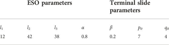
TABLE 2. Controller parameters
5.2 Simulation analysis under grid imbalance conditions
Based on the simulation model in Figure 9, simulation analysis is carried out under grid unbalance conditions. The system is charged and discharged, and each module, in turn, is run at its rated power to measure the stability and accuracy of the bus voltage and DC/DC converter output voltage and current during the charging and discharging of the different running power modules. The simulation conditions are as follows.
The four battery packs are rated at 50 V, 500 V, 1000 V, and 1600 V, respectively. When the DC/DC module is not running, the AC/DC is soft-started so that the bus voltage reaches 1650 V. The AC/DC runs continuously without output for 1 and 2 s. After 1 s, the phase voltage of one phase of the grid (phase B) is changed from 220 to 200 V to simulate a grid voltage imbalance. The following operation condition simulation tests are carried out.
1) The four DC-DC modules of the system are discharged at 350, 350, 200, and 125 A simultaneously for 1 s. After 3 rds, they are switched to −350, −350, −200, and −125 A simultaneously for 1 s. After the fourth second, DC-DC modules 1, 2, and 3 maintain the charging operation. DC-DC module 4 runs from −125 A discharge mode to 125 A charge mode for 1 s. The simulation waveform is shown in Figure 10A.
2) The battery packs of different voltage levels are charged and discharged several times under the above conditions. The steady-state bus voltage and current waveforms in charging and discharging mode on the output side are compared in Figure 10B.
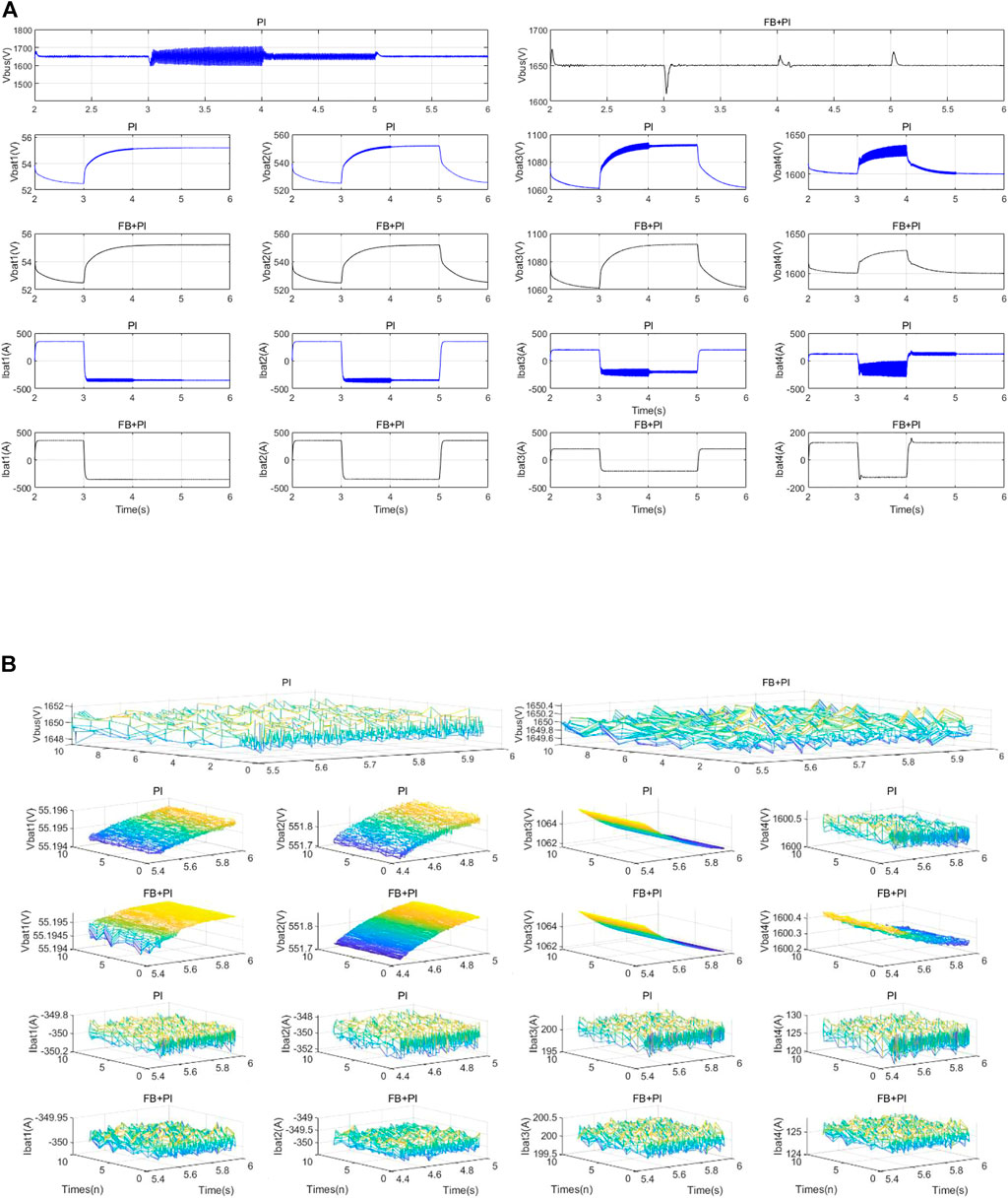
FIGURE 10. (A, B) Image A and B shows transient response and Steady-state control accuracy for each operating condition under grid imbalance in Figures 10 and grid normal in Figures 11, respectively.
Compared to the traditional PI double closed-loop control strategy, the control strategy proposed in this paper is less affected by grid imbalance and has better control accuracy. It also has better transient and steady-state characteristics. From the comparative analysis in Figure 10, under the grid unbalance condition, when the charging power is more significant, the corresponding bus voltage and battery voltage and current fluctuations on the output side become more extensive, which is consistent with the theoretical analysis.
5.3 Simulation analysis under normal grid conditions
Based on the simulation model in Figure 11, simulation analysis is carried out under grid normal conditions. The test methods are similar under normal and unbalanced conditions on the grid. The simulation conditions are as follows.
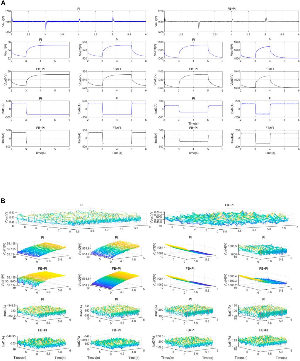
FIGURE 11. (A, B) shows the transient response under grid imbalance in the traditional double closed-loop control strategy in Figures 14 and under grid normal in the control strategy proposed in this paper in Figures 16, respectively.
The AC-DC module runs continuously without output for 1 s, and after 2 s, the following operating conditions are simulated and tested. When the DC/DC module is not running, the AC/DC is soft-started so that the bus voltage reaches 1650 V. The four battery packs are rated at 50 V, 500 V, 1000 V, and 1600 V, respectively.
1) The four DC-DC modules of the system are discharged at 350, 350, 200, and 125 A simultaneously for 1 s. After 3 rds, they are switched to −350, −350, −200, and −125 A simultaneously for 1 s. After the fourth second, DC-DC modules 1, 2, and 3 maintain the charging operation. DC-DC module 4 runs from −125 A discharge mode to 125 A charge mode for 1 s. After the fifth second, DC/DC modules 1 and 2 remain in charge operation, DC/DC module 4 remains in discharge operation and DC-DC module 3 runs from −200 A discharge mode to 200 A discharge mode for 1 s. The simulation waveforms are shown in Figure 11A.
2) The battery packs of different voltage levels are charged and discharged several times under the above conditions. The steady-state bus voltage and current waveforms in charging and discharging mode on the output side are compared in Figure 11B.
Steady-state characteristics compared to the traditional PI double closed-loop control strategy. The bus voltage, output-side voltage, and current control accuracy are higher during steady-state operation, which has a better transient. As seen from the comparative analysis in Figure 11, under the control strategy proposed in this paper, the bus voltage fluctuations are more minor during charging and discharging switching.
From the above simulation analysis, the voltage-current feedback control strategy proposed by this paper can be seen to effectively improve the suppression of bus voltage fluctuations and real-time tracking of external disturbances and grid uncertainties. Thus, it ensures that the requirements of high-precision voltage and current output under different operating conditions on the DC side are met.
6 Analysis of experimental results and conclusion
6.1 Experimental platform
To verify the effectiveness of the voltage–current feedforward control strategy proposed in this paper, the experimental platform is shown in Figure 12, and the practical system and control parameters are shown in Table 3.
1) The grid simulator as the AC source is adopted on the AC side, and it outputs 3-phase AC power connected with the DC-AC side of the high-precision power battery test equipment. The three-phase AC voltage with different voltage amplitudes, frequencies, and harmonic contents can be set according to the test conditions.
2) The three-level LCL topology is adopted on the DC-AC side of the high-precision power battery test equipment. The traditional bidirectional buck-boost topology, including four charge and discharge control channels, is assumed on the DC side. They could be connected independently or in parallel according to the load power needs.
3) PC1 represents the computer software supporting the high-precision power battery test equipment, which can edit the test steps related to different working modes according to the test needs. PC2 denotes the Modbus debugging interface of the DC-AC side, which can display the relevant operating information of the DC-AC side in real time and adjust the suitable control and protection parameters on the DC/AC side online.
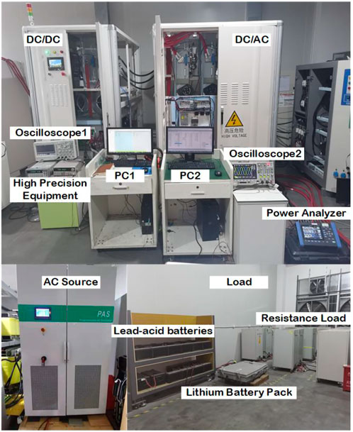
FIGURE 12. Experimental platform.
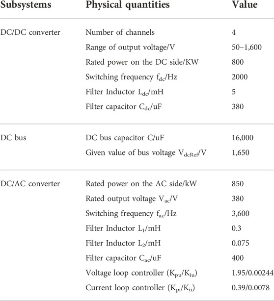
TABLE 3. Experimental system and controller parameters.
6.2 Grid voltage imbalance conditions
According to the three-phase voltage unbalance national standard, the negative sequence voltage unbalance should not exceed 2% during regular grid operation and should not exceed 4% for short periods [26]. The AC side of the experimental platform is connected to the grid simulator, and the grid voltage unbalance test condition is simulated by setting the output three-phase unbalanced AC voltage. The AC input voltage waveform under the unstable situation is shown in Figure 13. The DC side is connected to a Li-ion battery pack, and the battery is charged and discharged by setting the constant current charge and discharge test step through the host computer software. The current command is set to ±125 A. Under the grid voltage unbalance test condition, the bus control strategy is compared with the traditional PI double closed-loop bus control strategy and the proposed bus strategy of voltage-current feedforward. The output voltage and current and bus voltage waveforms are shown in Figure 14.

FIGURE 13. AC input voltage waveform under unbalanced grid conditions.
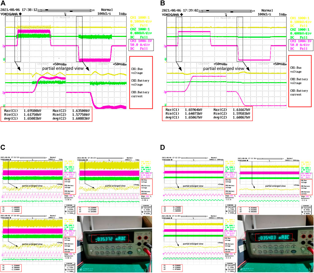
FIGURE 14. Output voltage, current waveforms, and bus waveforms during charging and discharging switching under unbalanced grid conditions ((A, B) shows the transient response under grid imbalance in the traditional double closed-loop control strategy in Figures 14 and under grid normal in the control strategy proposed in this paper in Figures 16, respectively, and (C, D) show the Steady-state control accuracy in the traditional double closed-loop control strategy and the control strategy proposed in this paper, respectively).
From the experimental waveform in Figure 14A, it can be seen that the traditional PI double-closed-loop bus control strategy leads to 2-fold frequency fluctuations in the bus voltage when the grid voltage is unbalanced, which is consistent with the theoretical analysis. The bus voltage fluctuation is approximately 40 V at the instant of charge and discharge switching. Figure 14B shows that there is no low-frequency fluctuation when the bus control strategy proposed in this paper is used during steady-state operation of the bus voltage, and the bus voltage fluctuation is approximately 10 V at the instant of charging and discharging switching.
As shown in Figure 14C, under the conventional PI double closed-loop bus control strategy, the charging current is set to −125 A. The peak steady-state bus voltage is 1.6 V (with 0.97‰ control accuracy), the peak output voltage is 1.35 V (with 0.84‰ control accuracy), and the peak output current is 0.11 A (with 0.88‰ control accuracy) during stable operation. At a particular moment, 124.86 A of the actual current value measured by Agilent’s high-precision existing test equipment (current sampling with an amplification ratio of 3530:1) could also be obtained.
Similarly, the charging current is set to −125 A in Figure 14D under the proposed bus control strategy. The peak steady-state bus voltage is 0.75 V (with 0.45‰ control accuracy), the peak output voltage is 0.55 V (with 0.34‰ control accuracy), and the peak output current is 0.05 A (with 0.40‰ control accuracy) during stable operation. At a particular moment, 124.972 A of the actual current value measured by Agilent’s high-precision existing test equipment (current sampling with an amplification ratio of 3530:1) could also be obtained.
The experimental results show that the bus control strategy proposed in this paper is used under unbalanced grid conditions. The bus voltage fluctuation amplitude is smaller during charging and discharging switching, and the bus voltage and output side voltage and current dynamic response performance are better. In steady-state operation, less than 0.5‰ control accuracy can be achieved.
A comparison of the steady-state control accuracy of each parameter under grid imbalance conditions is shown in Table 4.

TABLE 4. Steady-state control accuracy of each parameter under grid imbalance conditions.
6.3 Normal grid voltage conditions
Based on the experimental platform in the previous section, the grid voltage symmetrical operation condition is simulated by setting up the output of three proportional 380 V AC voltages. The AC input voltage waveform under balanced operation conditions is shown in Figure 15. The battery is charged and discharged using work steps edited by the upper computer software. The current command is set within a range from −125 A to +125 A.
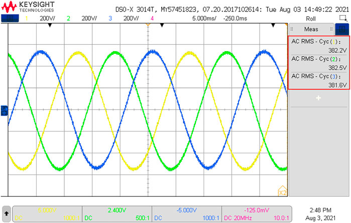
FIGURE 15. AC input voltage waveform under symmetrical grid conditions.
The output voltage and current and bus voltage waveforms during the grid voltage symmetrical test condition under the conventional PI double closed-loop bus control strategy and the proposed bus strategy based on voltage-current feedforward are shown in Figure 16.
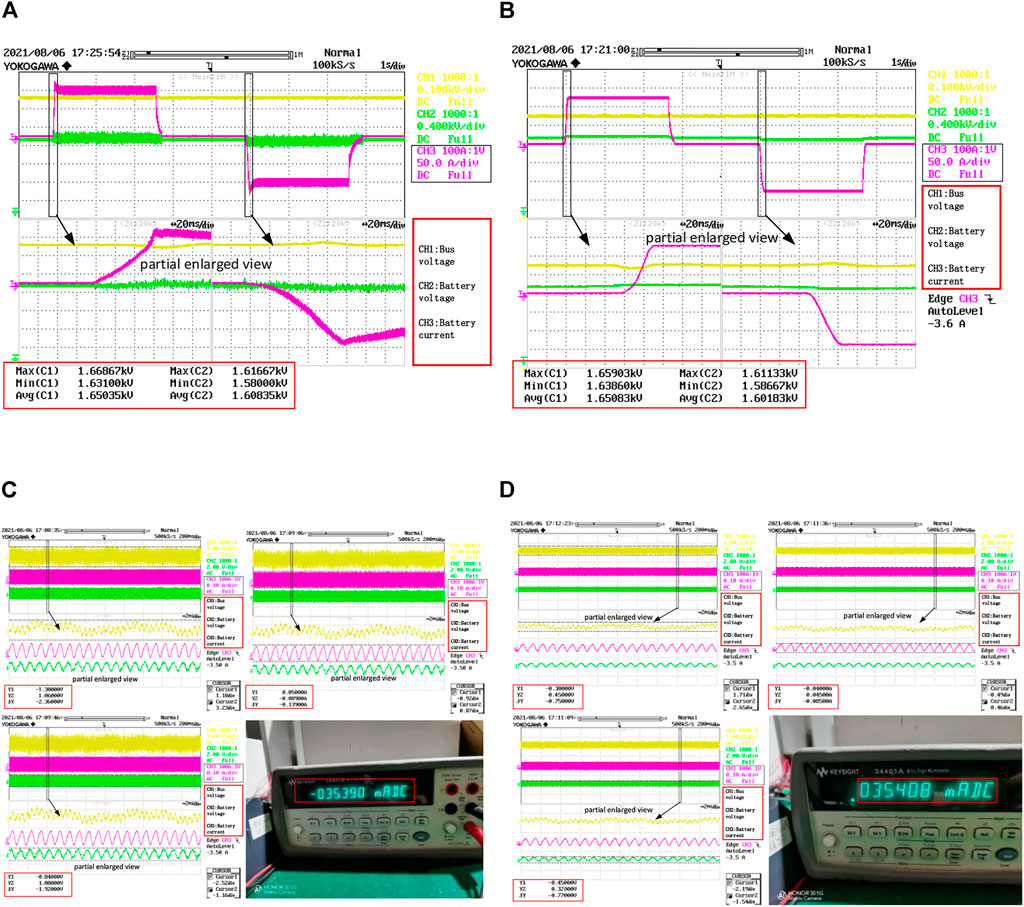
FIGURE 16. Experimental waveforms of output voltage, current, and bus during charging and discharging switching under symmetrical grid conditions ((A, B) shows the transient response under grid imbalance in the traditional double closed-loop control strategy in Figures 14 and under grid normal in the control strategy proposed in this paper in Figures 16, respectively. and (C, D) show the Steady-state control accuracy in the traditional double closed-loop control strategy and the control strategy proposed in this paper, respectively)..
In Figure 16A, when the traditional PI double closed-loop bus control strategy is used, the bus voltage fluctuation at the instant of charge and discharge switching is approximately 20 V. In Figure 16B, the bus control strategy proposed in this paper is used. The bus voltage fluctuation at the instant of charge and discharge switching is approximately 10 V, as seen in Figure 16C when the conventional PI double closed-loop bus control strategy with the current discharge command set to 125 A is used. The peak steady-state bus voltage is 1.3 V (with 0.79‰ control accuracy), the peak output voltage is 1.08 V (with 0.68‰ control accuracy), and the peak output current is 0.089 A (with 0.71‰ control accuracy) during stable operation. At a particular moment, 124.926 A of the actual current value measured by Agilent’s high-precision existing test equipment (current sampling with an amplification ratio of 3,530:1) could also be obtained. The discharging current is set to 125 A in Figure 16D under the proposed bus control strategy. In all, 0.65 V of the peak steady-state bus voltage, 0.45 V of the peak output voltage with 0.28‰ of the control accuracy, and 0.04 A of the peak output current with 0.32‰ of the control accuracy could be obtained during stable operation. At a particular moment, −124.990 A of the actual current value measured by Agilent’s high-precision existing test equipment (current sampling with an amplification ratio of 3,530:1) could also be obtained.
In Figures 16A,B in the experimental part of this paper, it can be seen that under the normal condition of the grid with the traditional PI control method, the response time of battery charging is approximately 60 ms. The response time of battery discharging is approximately 80 ms, while the response time of battery charging is approximately 20 ms, and the response time of battery discharging is approximately 20 ms under the bus voltage control method proposed in this paper.
The experimental results show that the bus control strategy proposed in this paper is used under normal grid conditions. The bus voltage fluctuation amplitude is smaller during charging and discharging switching. The dynamic response performance of the bus voltage, output-side voltage, and current improves. The bus voltage, output voltage, and current ripple are smaller during steady-state operation, resulting in a higher steady-state control accuracy of less than 0.5‰. Less ripple in bus voltage, output voltage, and current during steady-state operation could result in higher steady-state control accuracy, and the control accuracy is less than 0.5‰.
A comparison of each parameter’s steady state control accuracy under normal grid conditions is shown in Table 5.
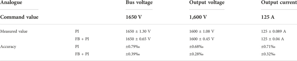
TABLE 5. Steady-state control accuracy of each parameter under regular grid operating conditions.
7 Conclusion
To address the impact of the dynamic response and steady-state control accuracy of the DC bus voltage during grid voltage unbalance and sudden changes in load current. This paper proposes a bus control strategy based on an expansive state observer with load current feedforward plus grid voltage second-order differential feedforward. The theoretical analysis and experimental results show that the system has the following characteristics.
1) By analysing the mechanism of bus voltage fluctuations caused by grid voltage imbalance and its harmonic components, a second-order differential feedforward of grid voltage is added to offset the impact of grid voltage disturbances on bus voltage fluctuations. Finally, the adaptability of the system to the grid is improved.
2) The load current observer based on a nonlinear expansion state observer with terminal sliding mode control features a simple design and no additional hardware sampling circuitry.
3) The theoretical analysis proves that the nonlinear expansion state observer can estimate the uncertainties and external disturbances of the system in real time, and the introduction of terminal sliding mode control enables the observation error to converge quickly to the specified sliding film surface. The rapidity and accuracy of the system for load current estimation are significantly improved.
4) Compared with the traditional double closed-loop control strategy under grid unbalanced or normal operating conditions, simulation and experimental results show that the proposed control method has the features of better control accuracy and transient and steady-state characteristics. Ma et al., 2018, Cao. and Ming, 2015.
Data availability statement
The original contributions presented in the study are included in the article/Supplementary Material, further inquiries can be directed to the corresponding author.
Author contributions
DX Conceptualization, Formal analysis, Methodology, Project administration, Supervision, Visualization, Writing–review editing LW Software, Validation, Writing–original draft ZZ Formal analysis SW Funding acquisition, Resources, Software LK Formal analysis JY Investigation.
Conflict of interest
LW, SW, and JY were employed by Guangdong HYNN Technologies Co., Ltd.
The remaining authors declare that the research was conducted in the absence of any commercial or financial relationships that could be construed as a potential conflict of interest.
Publisher’s note
All claims expressed in this article are solely those of the authors and do not necessarily represent those of their affiliated organizations, or those of the publisher, the editors and the reviewers. Any product that may be evaluated in this article, or claim that may be made by its manufacturer, is not guaranteed or endorsed by the publisher.
References
Aksenov, E. A., Yurkevich, V. D., and Zinoviev, G. S. (2016). “Current-sharing and DC bus voltage control system design of paralleled DC-DC converters,” in Proceedings of the2016 17th International Conference of Young Specialists on Micro/Nanotechnologies and Electron Devices (EDM), Erlagol, Altai Republic, 617–622.
Ali, M., Yaqoob, M., Cao, L., and Loo, K-H. (2021). Enhancement of DC-bus voltage regulation in cascaded converter system by a new sensorless load current feedforward control scheme. IET power electron. 14, 1457–1467. doi:10.1049/pel2.12123
Baazoug, N., Naouar, M. W., and Monmasson, E. (2018). “Design of an adaptive feedforward control scheme for the DC bus voltage control of single phase grid connected converters,” Proceedings of the2018 IEEE International Conference on Industrial Technology (ICIT), Lyon, Francein , 682–687.
Cao, X., Zhong, Q., and Ming, W. (2015). Ripple eliminator to smooth DC-bus voltage and reduce the total capacitance required. IEEE Trans. Ind. Electron. 62 (4), 2224–2235. doi:10.1109/tie.2014.2353016
Changchao, L., and Zhongjian, K. (2020). Synchronization control of complex network based on extended observer and sliding mode control. IEEE Access 8, 77336–77343. doi:10.1109/access.2020.2989895
Ding, B., Xu, D., Yang, W., Bi, K., and Yan, W. (2020). “Nonsingular terminal sliding mode control for PMLSM based on disturbance observer,” in Proceedings of the2020 IEEE 9th Data Driven Control and Learning Systems Conference (DDCLS), Suzhou, China, 850–854.
Fu, C., Zhang, C., Zhang, G., Song, J., Zhang, C., and Duan, B. (2022). Disturbance observer-based finite-time control for three-phase AC–DC converter. IEEE Trans. Ind. Electron. 69 (6), 5637–5647. doi:10.1109/TIE.2021.3088358
Geng, Y., Hou, M., Zhang, L., Dong, F., and Jin, Z. (2018). “An improved voltage control strategy for DC microgrid with hybrid storage system,” in Proceedings of the2018 13th IEEE Conference on Industrial Electronics and Applications (ICIEA), Suzhou, China, 958–962.
Henao-Bravo, E. E., Saavedra-Montes, A. J., Ramos-Paja, C. A., Bastidas-Rodriguez, J. D., and Gonzalez Montoya, D. (2020). Charging/discharging system based on zeta/sepic converter and a sliding mode controller for dc bus voltage regulation. IET Power Electron. 13, 1514–1527. doi:10.1049/iet-pel.2019.0746
Huang, Y., Yuan, X., Hu, J., Zhou, P., and Wang, D. (2016). DC-bus voltage control stability affected by AC-bus voltage control in VSCs connected to weak AC grids. IEEE J. Emerg. Sel. Top. Power Electron. 4 (2), 445–458. doi:10.1109/jestpe.2015.2480859
Hui, M., Shengyang, Y., Wei, W., and Wang, S. (2019). “The PR control with load current feedforward for vienna rectifier,” in Proceedings of the2019 IEEE International Conference on Power, Intelligent Computing and Systems (ICPICS), , Shenyang, China., 508–512.
Isik, S., Alharbi, M., and Bhattacharya, S. (2018). “A feedforward current control strategy for a MMC based point to point HVDC systems,” in Proceedings of the2018 9th IEEE International Symposium on Power Electronics for Distributed Generation Systems (PEDG), Charlotte, North Carolina, 1–8.
Jamma, M., Bennassar, A., Akherraz, M., Fahassa, C., Barara, M., and Oproescu, M. (2017). “Self-tuning fuzzy PI dc-bus voltage controller and fuzzy switching sequences selection for direct power control of PWM AC/DC converter,” in Proceedings of the2017 9th International Conference on Electronics, Computers and Artificial Intelligence (ECAI), Targoviste, Romania., 1–6.
Leal, W. C. (2017). “A control system for battery current sharing in DC microgrids with DC bus voltage restoration,” in Proceedings of the2017 Brazilian Power Electronics Conference (COBEP), Juiz de Fora, Brazil, 1–6.
Li, X., Guo, L., Zhang, S., Wang, C., Li, Y. W., Chen, A., et al. (2018). Observer-based DC voltage droop and current feedforward control of a DC microgrid. IEEE Trans. Smart Grid, 9. 5, 5207–5216. doi:10.1109/tsg.2017.2684178
Liang, C., Zhang, Y., Ji, X., Meng, X., An., Y., and Yao, Q. (2019). “DC bus voltage sliding-mode control for a DC microgrid based on linearized feedback,” in Proceedings of the 2019 Chinese Automation Congress (CAC), Hangzhou, China, 5380–5384.
Ma, D., Lin, S., Cheng, Q., and Sun, Q. (2018). “The DC bus voltage control based on virtual inertia for SST,” in Proceeding of the 2018 IEEE 7th Data Driven Control and Learning Systems Conference (DDCLS), Enshi, China, 575–580.
Wang, C., Li, X., Guo, L., and Li, Y. W. (2014). A nonlinear-disturbance-observer-based DC-bus voltage control for a hybrid AC/DC microgrid. IEEE Trans. Power Electron. 29 (11), 6162–6177. doi:10.1109/tpel.2013.2297376
Wang, Z., Li, Y., Yuan, X., Liu, R., Li, Z., and Shi, M. (2020). “An improved current feedforward control strategy for multi-port power electronic transformer,” in Proceedings of the2020 IEEE 9th International Power Electronics and Motion Control Conference (IPEMC2020-ECCE Asia), 3100–3106.
Wu, H., Han, M., and Sun, K. (2019). Dual voltage rectifier based single phase AC-DC converters with dual DC bus and voltage-sigma architecture for variable DC output applications. IEEE Trans. Power Electron. 34 (5), 4208–4222. doi:10.1109/tpel.2018.2864584
Xiong, Y., and Ye, Y. (2019). Physical interpretations of grid voltage full feedforward for grid-tied inverter. IEEE Trans. Circuits Syst. Ii. 66 (2), 267–271. doi:10.1109/tcsii.2018.2850041
Zhang, L., and Ruan, X. (2019). Control schemes for reducing second harmonic current in two-stage single-phase converter: An overview from DC-bus port-impedance characteristics. IEEE Trans. Power Electron. 34 (10), 10341–10358. doi:10.1109/tpel.2019.2894647
Zhao, Z., Hu, J., and Chen, H. (2017). “Bus voltage control strategy for low voltage DC microgrid based on AC power grid and battery,” in Proceedings of the2017 IEEE International Conference on Energy Internet (ICEI), Beijing, China, 349–354.
Keywords: power battery test equipment, AC/DC, DC bus voltage controller, ESO, second order differential feed-forward
Citation: Xie D, Wang L, Zhang Z, Wang S, Kang L and Yao J (2023) High-precision bus voltage control based on NLESO and TSMC predicted load current and grid voltage differential feedforward. Front. Energy Res. 10:1009981. doi: 10.3389/fenrg.2022.1009981
Received: 02 August 2022; Accepted: 14 September 2022;
Published: 31 January 2023.
Edited by:
Chun Wei, Zhejiang University of Technology, ChinaReviewed by:
Mingfei Ban, Northeast Forestry University, ChinaJingang Han, Shanghai Maritime University, China
Qinglei Bu, Xi’an Jiaotong-Liverpool University, China
Copyright © 2023 Xie, Wang, Zhang, Wang, Kang and Yao. This is an open-access article distributed under the terms of the Creative Commons Attribution License (CC BY). The use, distribution or reproduction in other forums is permitted, provided the original author(s) and the copyright owner(s) are credited and that the original publication in this journal is cited, in accordance with accepted academic practice. No use, distribution or reproduction is permitted which does not comply with these terms.
*Correspondence: Di Xie, dixie-0728@outlook.com; Liangliang Wang, wanglljx@foxmail.com