Three-phase boost-stage coupled current source inverter concept and its space vector modulation
 Weiqi Wang
 Xinian Li2
 - 1College of Electrical Engineering and Automation, Shandong University of Science and Technology, Qingdao, China
- 2School of Information and Electronic Engineering, Shandong Technology and Business University, Yantai, China
- 3State Grid Shandong Electric Power Company, Qingdao, China
The current source inverter (CSI) is essentially a converter with inherent boost capability and has been preliminarily applied in the field of renewable energy generation systems. However, conventional CSIs are mostly operated independently. Several existing multilevel CSI topologies entirely rely on parallel combinations, which seems to be not very suitable for capacity expansion. To solve this issue, this paper proposes a concept of three-phase boost-stage coupled current source inverter (BSC-CSI) through the duality principle, which can output multi-level currents with a reduced number of switches as well as hardware costs. Compared with the state-of-the-art CSIs, the proposed BSC-CSI can notably simplify the implementation of the multi-level modulation scheme and meanwhile ensure the power devices switch under lower current stress. To further take full advantage of the modularity and scalability, the BSC-CSI can be constructed by hybrid using silicon-carbide (SiC) and silicon (Si) based semiconductor switches for improving efficiency. The experimental results have verified the theoretical findings.
1 Introduction
With the increasing attention paid to clean energy, power inverter has become the key component of modern renewable energy network. Generally, power inverters can be classified as voltage source inverter (VSI) and current source inverter (CSI). Although VSI currently dominates the application market, CSI draws scholars’ continuous attention and has been considered to be a promising topology. CSI is well known for its inherent short-circuit protection advantage and voltage boost capability, which have been proven to be of the essence and important for grid applications and renewable energy generations. Therefore, it has been used in certain application fields, such as renewable energy systems, active power filters, and some high-power drives (Nishikata and Tatsuta, 2010; Guo, 2017a; Liu et al., 2020). However, CSI still faces the practical challenges of high power loss, bulky inductance, and huge space occupation.
To solve these problems, scholars tried to apply high-performance semiconductor switches, e.g. the reverse blocking IGBTs (RB-IGBTs), silicon-carbide (SiC), and gallium nitride (GaN) based MOSFETs (Su and Tang, 2011; Guacci et al., 2019; Narasimhan et al., 2021). However, these attempts strictly depend on the high investment, so there is still a big gap between hardware all-upgrade solutions and the actual applications. In terms of the three-phase topology innovations, the H7-CSIs have carried out valuable thoughts on reducing switching loss (Guo, 2017b; Wang et al., 2018; Lorenzani et al., 2019), but limited by the power range of the shunt-connect device, they seem to be weaker for high-power applications. For large-scale power fields, the multi-level technique can be a great added value to CSI topologies (Wu, 2006). Multi-level current source inverter (MCSI) is considered to be an effective technology to reduce the switching stress as well as the filter size and has been extensively implemented, e.g. the single/multi-rating inductor MCSI, the paralleled H-bridge MCSI, and the buck-boost MCSI (Gao et al., 2010; Dupczak et al., 2012; Ries and Heldwein, 2020; Alskran and Simoes, 2021; Ding and Li, 2021). However, these state-of-the-art research works are essentially the series/parallel combinations of multiple H6 bridges, which can be classified as the H6-type MCSIs. And they not only inherit the common problems of conventional CSI, but also face the critical disadvantages of the increasing number of components and operational complexity. Therefore, CSI right now still needs a simple, compact and cost-efficient implementation solution.
At the same time, the multi-level voltage source inverters (MVSIs) have been well extensively investigated and implemented for over a decade. When the research perspective of the multi-level technique returns to VSI, it can be easily found that MVSIs have much clearer topological evolution paths, e.g. neutral point clamped (NPC) MVSI (Rodriguez et al., 2010; Wang et al., 2013), flying capacitor (FC) MVSI (He and Cheng, 2016), and cascaded H-bridge (CHB) MVSI (Yu et al., 2016). Among them, the NPC MVSI is one of the most commonly used MVSI topology types, and features a relatively high degree of integration. Inspired by the I-type NPC MVSI structure, this paper proposes a concept of three-phase boost-stage coupled CSI (BSC-CSI), explains its construction rules and operational principles, and further illustrates the space vector modulation (SVM) scheme. The proposed BSC-CSI concept, on the one hand, can effectively reduce the complexity of MCSI as well as the number of components, and on the other hand, can also improve CSI efficiency with an acceptable cost. Besides, the BSC-CSI concept can even integrate some other existing research results of CSI topologies.
This paper is organized as follows. In Section 2, the existing MCSI topologies are first introduced and parsed, while the topological construction mechanism of I-type NPC MVSI is analyzed. And then, with the insight of dual principle, the concept of BSC-CSI is proposed. In Section 3, the compatible SVM strategy is presented in detail. The operational characteristics are also analyzed. Finally, simulation and experimental tests are presented to verify the theoretical findings.
2 Topology of the three-phase boost-stage coupled CSI
2.1 Comparison of multi-level construction mechanism
The basic purpose of multi-level technique is to reduce down the power stress of switches, with the added benefit of improving power quality. As for an MCSI, the significance of reducing the current is not only to reduce the power loss of switches, but also to meet the line loss constraints of the constant current transmission mode. To fulfill this requirement, most existing three-phase MCSIs adopt multi-module integration technology, which has built several types. Figure 1 demonstrates their topologies, which takes five-level MCSI as examples.
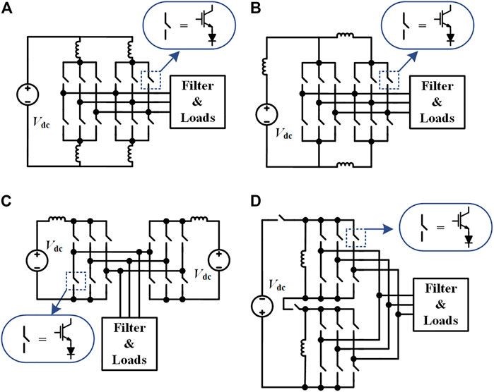
FIGURE 1. (A) Single-rating inductor MCSI (B) Multi-rating inductor MCSI. (C) Paralleled H-bridge MCSI. (D) Buck-boost MCSI.
Figure 1A shows the single-rating inductor MCSI (SI-MCSI). It has two H6 converter sub-modules and four inductors with the same current rating. Their DC inputs come from the same DC rail, while the AC outputs inject current into the load in parallel. The multi-rating inductor MCSI (MI-MCSI) is one variant of the SI-MCSI, which is shown in Figure 1B. The main difference is the non-uniform inductors used to split the input current. Both SI-MCSI and MI-MCSI have the drawback of circulating current, and it is difficult to control the power fluctuation of each single module. The paralleled H-bridge MCSI (PH-MCSI), as shown in Figure 1C, can solve this problem. It utilizes two independent current sources to decouple the power control of the sub-modules. However, the requirement of equal current supply seriously affects the practical value of this topology. Figure 1D shows the Buck-boost MCSI. It mainly aims at a wide range of output voltage, but lacks the ability to handle high current applications.
As it can be found from the above MCSI, their topology is essentially a series-parallel combination of the H6 converter sub-modules. The modulation process is mainly to control the switching combinations of every H6 converter sub-modules. If there are n resembled sub-modules, MCSI will have 6n power switches and 6n power diodes, to realize the 2n+1 level output phase current. And the total number of the switching combinations will be 6n. Therefore, with the increase of the current level, these MCSI solutions will have huge hardware costs as well as space occupation, and there exists a great difficulty in modulation implementation, e.g., 5-level CSI has 12 switches with 81 switching combinations, and 7-level CSI has 18 switches with 729 switching combinations.
When the research perspective is shifted back to MVSIs, it can be found that the construction form of topology is completely different. The I-type NPC MVSI, for example, has no integration of three-phase modules in its topology, but its voltage-level generation mechanism is quite clear. The I-type NPC MVSIs mainly include the diode neutral point clamped (DNPC) MVSI and active neutral point clamped (ANPC) MVSI which are commonly used in industry. Their topologies with 3-level outputs as an example are shown in Figure 2.
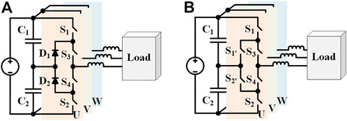
FIGURE 2. (A) I-type DNPC MVSI. (B) I-type ANPC MVSI.
Both DNPC MVSI and ANPC MVSI integrate capacitor on the DC rail to provide the extra voltage levels in addition to the DC bus. And the output of each phase is connected to the DC bus through several switches whose essential function is to select the voltage state of the output of AC side. The main difference between DNPC MVSI and ANPC MVSI is that ANPC MVSI replaces the diodes (D1 and D2 in DNPC MVSI) with two power switches (S1’ and S2’). They can provide the capability to actively control the potential of the neutral point.
As shown in Figure 2B, from the perspective of each phase, ANPC MVSI can be divided into two parts. Except the power supply, the front-end circuit is composed of two capacitors and four switches (S1, S1’, S2, and S2’), which can provide 3-level voltages, while the rear-end circuit is composed of two switches (S3 and S4) with one inductive filter, which can realize the output of each phase. This structural feature can be applied to DNPC MVSI as well, i. g. the front-end circuit is responsible for voltage levels, which includes C1, C2 S1, S2, D1 and D2, and the rear-end circuit uses S3 and S4 to implement the phase outputs.
2.2 Duality principle and the BSC-CSI topology
Duality is one of the common basic characteristics among circuitries and is of importance and mathematical insights. In graph theory, one converter can be abstracted as a graph composed of nodes and edges, which have been introduced in (Li and Li, 2020).
For a planar graph, in addition to the typical electrical duality (e.g., voltage/current sources and inductive/capacitive components), geometrical duality can also be used to find out its dual topology, which can be clearly seen between Buck and Boost converters, as well as that between single-phase VSI and CSI.
As for a non-planar graph, it may be necessary to use the Quasi-dual method (dual on each active switching state) to find its dual topology. A typical representative of this method is the duality between three-phase VSI and CSI, whose topologies are shown in Figure 3. It is worth noting that the power switch in VSI needs to reverse parallel with a power diode, which can sustain the reverse power flow path, while by contrast, the power switch in CSI must series connect with a power diode so as to provide the reverse-blocking capability. Besides, the voltage/current level between VSI and CSI is not consistent, e.g., 2-level VSI is dual to 3-level CSI.
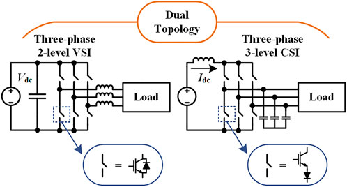
FIGURE 3. Duality between conventional three-phase VSI and CSI.
The above findings are a brief summary of the duality characteristics of the frequently-used converters. Following a similar approach, clues can be explored for constructing new CSIs with reduced switches. In order to facilitate the study of topology evolution, we can first study the simplest MCSI, i. g. starting from the new construction method of 5-level CSI topology. Therefore, its dual prototype can select with the I-type three-phase NPC 3-level VSI.
On the basis of topological analysis in Section 2.1, if take the rear-end output of one phase as a whole, then the front-end structure of one phase in ANPC 3-level VSI can be abstracted as a graph. Through the geometrical duality method, its dual topology can be found. This duality process is shown in Figure 4. The letters (A-E) are the nodes of the ANPC front-end phase module. The circled numbers represent the meshes of the planar graph and can be mapped as the new nodes of the dual topology. In the same way, the dual structure of DNPC can be obtained, as shown in Figure 5.
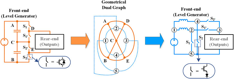
FIGURE 4. Graphs of ANPC phase module and its duality topology.
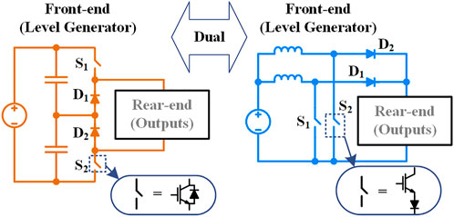
FIGURE 5. Graphs of DNPC phase module and its duality topology.
In light of the above research results, a multi-level current source generator can be constructed by expanding the front-end structure into multiple branches in parallel. As for the rear-end circuit, since its essential function is to commutate the phase current output, if referring to the commutation structure of conventional CSI, then the topology of the proposed three-phase boost-stage coupled CSI can be obtained, which is demonstrated in Figure 6.

FIGURE 6. Topology of the proposed BSC-CSI.
The front-end stage of BSC-CSI contains n T-type boost branches, and each one needs an inductor to store energy and provide constant DC current. The power diodes (D7-x and D8-x) are responsible for preventing backflow current. The shunt-connected switches (S7-x) can provide a shoot-through channel, and the series-connected switches (S8-x) are employed to decouple the connection between the inductor current and the branch’s output, which need to be operated complementary to S7-x, thereby synthesizing the output current level of the front-end stage.
To go a step further, it can be observed that the existing H7-CSI topology is actually one special form of the BSC-CSI (Wang et al., 2018), which only contains one T-type boost branch and omitted the series power diode. More specifically, as reported in (Wang et al., 2015), when the power factor angle of the AC load is less than 30°, S7-x can independently implement the shoot-through function. Therefore, S8-x can be omitted under this load condition, and thus can be regarded as a dual topology derived from the DNPC 3-level VSI.
3 Modulation of the three-phase boost-stage coupled CSI
3.1 Space vector modulation scheme
As described above, the T-type boost branches are in charge of the current injection to the rear-end circuit, and the rear-end H6 bridge is responsible for the phase commutation. Therefore, only when they are well-operated and coordinated, can the whole inverter obtain the correct multi-level output current. To realize the compatible space vector modulation of the proposed BSC-CSI, all the existing space vectors together with their corresponding switching combinations should be listed for the inverter first. Then, in order to synthesize the reference, space vectors must be appropriately selected, which is the key issue in the process of designing the modulation strategy. Next, the dwell time of each selected space vector should be calculated correctly. At last, it is necessary to design the switch combination sequence of the modulation period to optimize the performance of the whole inverter.
In order to accomplish the SVM design tasks, three basic principles should always be followed:
a) To reduce the output harmonics, the nearest space vectors should be priority selected.
b) To suppress switching losses, the rear-end power switches (S1-S6) are preferably operated with lower current stress.
c) To ensure the balance of each front-end T-type branches, the shunt-connected switch (S7-x) should be operated equally in one modulation period.
The general method to select the proper nearest space vectors to synthesize the reference, is to find a triangular region that is composed of the three nearest space vectors and covers the target reference. This process is illustrated in Figure 7. Let three arbitrary vectors (
where na and nb are the distances of the endpoints between two adjacent vectors.
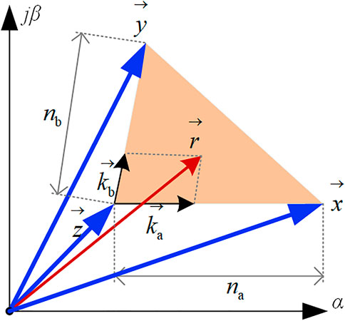
FIGURE 7. Synthesizing the target reference with three arbitrary vectors.
Taking 7-level BSC-CSI as an example, which consists of 3 T-type boost branches and one H6 bridge, For simplicity of illustration, S8-1, S8-2, and S8-3 are omitted from this example since they only work under special load conditions. The overall space vector diagram is shown in Figure 8A. Denote turning ON all of {S7-1, S7-2, S7-3} as TOA, while TO2 refers to turning ON any two of {S7-1, S7-2, S7-3}, TO1 refers to turning ON any one of {S7-1, S7-2, S7-3}, and NULL is to turn off them all. The switching states are summarized in Table 1, where only turn-ON switches are listed, and Idc represents the total DC current.
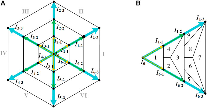
FIGURE 8. (A) Overall space vector diagram. (B) Region divisions of Sector I.
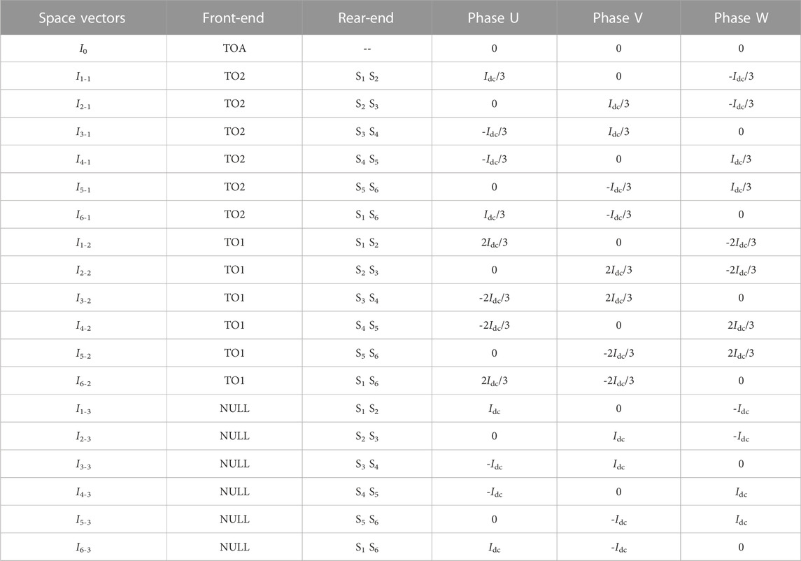
TABLE 1. Space vectors and switching states of BSC-CSI (7-level).
As shown in Table 1; Figure 8A, there are 19 potentially available space vectors in the proposed 7-level BSC-CSI: six large vectors, six medium vectors, six small vector and only one zero vector. In light of the above principles and considerations, the SVM scheme of 7-level BSC-CSI is proposed to partition each sector into nine regions, which is shown in Figure 8B. Thus, the overall space vector diagram of 7-level BSC-CSI can be divided into 54 regions.
As exemplified in Figure 8B for Sector I, the segmented nine regions are divided by the angle bisector and the connecting lines between vector endpoints. And the working state of the inverter can be classified into three modes: Mode 1 (reference locates in region 1 with 3-level switched currents), Mode 2 (reference rotates among region two to four with 5-level switched currents), and Mode 3 (reference rotates among region five to nine with 7-level switched currents). It is worth noting that these regions are symmetric about the angle bisector of Sector I.
Region one only contains I0, I1-1, and I6-1, its SVM pattern can be considered the same as the H7-CSI, whose switching sequence can ensure the zero current switching (ZCS) for rear-end switches (S1-S6). When the inverter is operated in Mode 2, the reference can be synthesized by small vectors and medium vectors, so that the rear-end switches (S1-S6) can be operated with Idc/3. To be more specific, Region 2 uses I1-1, I6-1, and I6-2 to synthesize the reference vector, while I1-1, I6-1, I1-2, and I6-2 are employed in Region 3, where I1-1 and I6-1 should theoretically have the same dwell time. In Mode 3, the reference is synthesized in a slightly complicated way, whose selected vectors include small vectors, medium vectors, and large vectors. Region 5 uses I1-1, I6-2, and I6-3 to synthesize the reference, and the rear-end switches (S1-S6) are switched with Idc/3. Region six includes I1-2, I6-2, and I6-3, while Region 7 uses I1-2, I6-2, I1-3, and I6-3 to synthesize the reference, where I1-2 and I6-2 have the same dwell time. Both Region six and Region seven can switch rear-end switches (S1-S6) with 2Idc/3. The composition space vectors of reference in all the nine regions together with their dwell times are listed in Table 2, where ma is the modulation index.
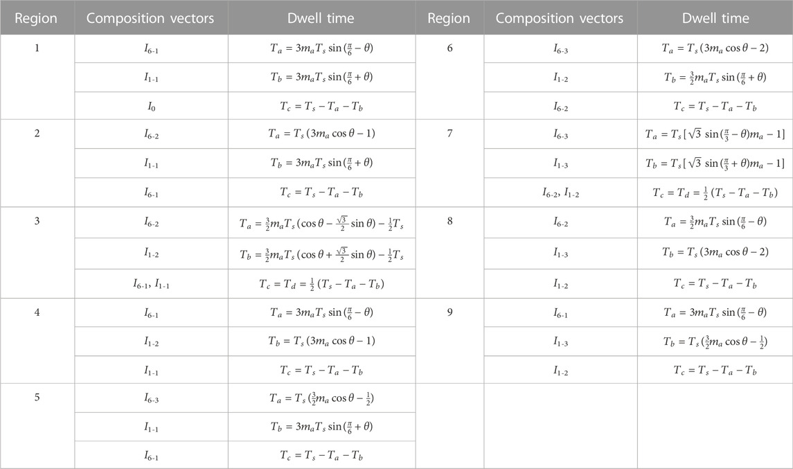
TABLE 2. Composition vectors of reference in sector I.
As for the switching sequences, the front-end switches (S7-1, S7-2, and S7-3) should be arranged carefully to keep the T-type branches balance. It should be pointed out that if all the T-type-branch inductors are of the same value, the actual switching operations of S7-1, S7-2, and S7-3 should be treated equally. They will not only occupy the same dwell time during one modulation period, but also evenly be distributed in the switching cycle. In order to achieve this feature, the switching sequences of the proposed SVM scheme can take the symmetrical pattern with three possible models, which are illustrated in Figure 9. Ts is the modulation period. A and B represent two switching states of the front-end stage. For different regions, the two switching states should accordingly be implemented with different switching combinations. These operational arrangements can take advantage of the bypass function of the front-end T-type branches to reduce the switching current stress of the rear-end switches (S1-S6).

FIGURE 9. The models of switching sequences (in Sector I).
3.2 Operational feature benchmarking
The proposed BSC-CSI has some unique characteristics in terms of the number of switching devices and power loss. Taking 7-level as an example, the comparisons between the conventional H6-type MCSI and the proposed BSC-CSI (S8-x omitted) are listed in Table 3, where “R.” is short for “Region”, and “ZCS” is short for “zero current switching”.

TABLE 3. Comparisons between the H6-type MCSI and the proposed BSC-CSI (7-level).
The power-switch count of the proposed BSC-CSI has reduced by half. And its number of switching combinations is obviously less than that of the conventional H6-type MCSI, which makes the modulation strategy much easier to implement.
As for the modulation operation, the front-end switches are constantly operated with Idc/3, while the switching current stress of rear-end switches depends on the actual modulation index and reference’s location. Besides, the BSC-CSI also has a significant advantage in switching counts, which makes a lower switching loss. The current rating through front-end switches is one-third of that in rear-end switches. This feature enables BSC-CSI to configure the rear-end with relatively high power but cheap devices and meanwhile to use the front-end with high-performance devices with a low current rating. Intuitively, it gives the possibility to improve efficiency by only using SiC devices for front-end switches, which can make it cost-effective customization. It is worth noting that other-level BSC-CSIs have similar characteristics in terms of configuration and switching operations.
4 Experimental results
To validate the performance of the proposed BSC-CSI and its modulation scheme, a 7-level BSC-CSI experimental prototype has been built, which is shown in Figure 10. The control board is integrated with a DSP (TMS320F28335 of Texas Instruments) and an FPGA (xc3s500e of XILINX). Among them, the DSP is used to calculate the dwell times and to judge the region of reference vector, while the FPGA is responsible for the switching selection and the arrangements of driving sequence. On the power board, in order to obtain a cost-effective performance, the front-end switches (S7-1, S7-2, and S7-3) are employed with SiC-MOSFETs (C2M0160120D of CREE), and the rear-end switches (S1-S6) are Si-IGBTs (IKW20N60T of Infineon). Besides, all the power diodes are C2D20120D from CREE. The DC power supply is employed with Delta SM 600–10. Other experimental parameters are listed in Table 4
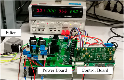
FIGURE 10. Experimental prototype of the proposed BSC-CSI.
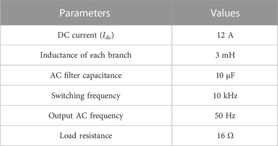
TABLE 4. Parameters of the experimental prototype.
Employed with the proposed space vector modulation scheme, the driving pulses of switches (S2, S6, S7-1, S7-2) are captured in Figure 11. It is obvious that the front-end power switches (S7-x) of BSC-CSI are switched more frequently than the other switches (S1-S6). Because S7-x is configured with SiC-MOSFETs, this high switching frequency will not result in the heavy burden of switching loss.
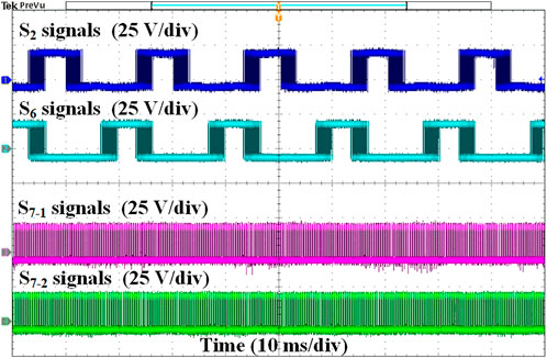
FIGURE 11. Driving pulses of switches (S2, S6, S7-1, S7-2).
In order to demonstrate and verify the working characteristics of the proposed BSC-CSI in different modes, the modulation index is set to 0.5 and 0.9, respectively. And the corresponding experimental results (output voltages, switched current, and inductor currents) are shown as Figures 12, 13.
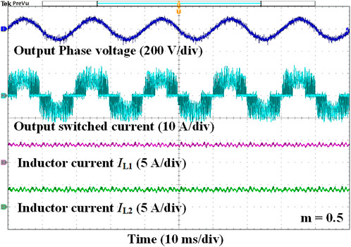
FIGURE 12. Experimental waveforms of output phase voltage, output switched current, and inductor currents under m = 0.5.
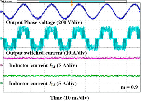
FIGURE 13. Experimental waveforms of output phase voltage, output switched current, and inductor currents under m = 0.9.
When the modulation index is 0.5, the reference will rotate among the medium vectors (green vectors of Figure 8A), and the BSC-CSI prototype outputs the five-level switched current. The output phase voltage performs 50 Hz sinusoidal waveform with the amplitude of 96 V. The inductor currents show the power balance of each front-end branches. This phenomenon is consistent with the expectation of the design in Section 3.1.
When the modulation index is fixed up to 0.9, the reference will rotate among the large space vectors (blue vectors of Figure 8A), and the output results clearly presents the seven-level switched current. As expected, the proposed BSC-CSI can properly output 50 Hz sinusoidal waves, whose amplitude is about 172 V. And the inductor current of each T-type branch keeps balancing at about 4 A.
To validate the efficiency performance, an additional prototype of conventional H6-type 7-level CSI has been built up using the same experimental parameters. Except for the SiC-MOSFETs of BSC-CSI, all the other power devices are employed with the same hardware. Both the H6-type 7-level CSI and the 7-level BSC-CSI were tested under the same conditions. In accordance with a series of operating power points, efficiency data is recorded using a power analyzer (PM6000 of Voltech). Their efficiency carves are shown in Figure 14.
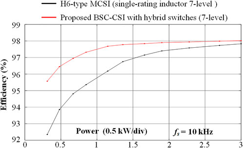
FIGURE 14. Efficiency comparison of the two experimental prototypes.
The comparison results show that the 7-level BSC-CSI achieves a relatively higher efficiency over the conventional H6-type 7-level CSI. However, this efficiency promotion has a tendency to weaken as the power increases. It is mainly because the proportion of conduction loss in the total loss will gradually increase as the modulation index increases, thereby weakening its advantages in reducing the switching loss.
5 Conclusion
This paper proposes a concept of three-phase boost-stage coupled CSI and establishes the compatible space vector modulation scheme. The BSC-CSI concept shows a new duality path through NPC VSIs to construct CSI topologies and can cover up the previously investigated H7-CSI topology. Compared with state-of-the-art MCSI, the proposed BSC-CSI has fewer switching components, making the whole converter more compact, and the implementation method of SVM can be simplified significantly. Moreover, with the customization of cost-efficient hybrid switches, the proposed SVM scheme is able to ensure BSC-CSI to perform a higher efficiency. The corresponding performance has been validated through experimental tests.
Data availability statement
The original contributions presented in the study are included in the article/supplementary material, further inquiries can be directed to the corresponding author.
Author contributions
WW substantially contributed to the conception of the study, SR helped perform the analysis with constructive discussions, XL and XX conducted supervision. All authors have read and agreed to the published version of the manuscript.
Funding
This research was supported by State Grid Shandong Electric Power Company under Grant No. 520602210002. The authors declare that the funder was not involved in the study design, collection, analysis, interpretation of data, the writing of this article, or the decision to submit it for publication.
Conflict of interest
Author SR was employed by the State Grid Shandong Electric Power Company.
The remaining authors declare that the research was conducted in the absence of any commercial or financial relationships that could be construed as a potential conflict of interest.
Publisher’s note
All claims expressed in this article are solely those of the authors and do not necessarily represent those of their affiliated organizations, or those of the publisher, the editors and the reviewers. Any product that may be evaluated in this article, or claim that may be made by its manufacturer, is not guaranteed or endorsed by the publisher.
References
Alskran, F., and Simoes, M. (2021). Multilevel current source converter-based STATCOM suitable for medium-voltage applications. IEEE Trans. Power Deliv. 36, 1222–1232. doi:10.1109/TPWRD.2020.3004419
Ding, L., and Li, Y. (2021). Multilevel CSC system based on series–parallel connected three-phase modules with optimized carrier-shift SPWM. IEEE Trans. Power Electron. 36, 3957–3966. doi:10.1109/TPEL.2020.3021392
Dupczak, B., Perin, A., and Heldwein, M. (2012). Space vector modulation strategy applied to interphase transformers-based five-level current source inverters. IEEE Trans. Power Electron. 27, 2740–2751. doi:10.1109/TPEL.2011.2177479
Gao, F., Loh, P., Blaabjerg, F., and Vilathgamuwa, D. (2010). Five-level current-source inverters with buck–boost and inductive-current balancing capabilities. IEEE Trans. Ind. Electron. 57, 2613–2622. doi:10.1109/TIE.2009.2030208
Guacci, M., Zhang, D., Tatic, M., Bortis, D., Kolar, J., Kinoshita, Y., et al. (2019). Three-phase two-third-PWM buck-boost current source inverter system employing dual-gate monolithic bidirectional GaN e-FETs. CPSS Trans. Power Electron. Appl. 4, 339–354. doi:10.24295/CPSSTPEA.2019.00032
Guo, X. (2017). A novel CH5 inverter for single-phase transformerless photovoltaic system applications. IEEE Trans. Circuits Syst. Ii. 64, 1197–1201. doi:10.1109/TCSII.2017.2672779
Guo, X. (2017). Three-phase CH7 inverter with a new space vector modulation to reduce leakage current for transformerless photovoltaic systems. IEEE J. Emerg. Sel. Top. Power Electron. 5, 708–712. doi:10.1109/JESTPE.2017.2662015
He, L., and Cheng, C. (2016). A flying-capacitor-clamped five-level inverter based on bridge modular switched-capacitor topology. IEEE Trans. Ind. Electron. 63, 7814–7822. doi:10.1109/TIE.2016.2607155
Li, Y., and Li, Y. (2020). Power converters topological transformation using dual and isomorphic principles. IEEE Open J. Power Electron. 1, 74–87. doi:10.1109/OJPEL.2020.2981653
Liu, P., Wang, Z., Song, Q., Xu, Y., and Cheng, M. (2020). Optimized SVM and remedial control strategy for cascaded current-source-converters-based dual three-phase PMSM drives system. IEEE Trans. Power Electron. 35, 6153–6164. doi:10.1109/TPEL.2019.2952672
Lorenzani, E., Migliazza, G., Immovilli, F., and Buticchi, G. (2019). CSI and CSI7 current source inverters for modular transformerless PV inverters. Chin. J. Electr. Eng. 5, 32–42. doi:10.23919/CJEE.2019.000009
Narasimhan, S., Anurag, A., and Bhattacharya, S. (2021). “Comparative study of a 3.3 kV SiC-based voltage and current source inverter for high-speed motor drive applications,” in Proc. in 2021 IEEE 12th Energy Conversion Congress & Exposition - Asia (ECCE-Asia), Singapore, 24-27 May 2021, 2211–2217. doi:10.1109/ECCE-Asia49820.2021.9479066
Nishikata, S., and Tatsuta, F. (2010). A new interconnecting method for wind turbine/generators in a wind farm and basic performances of the integrated system. IEEE Trans. Ind. Electron. 57, 468–475. doi:10.1109/TIE.2009.2026765
Ries, L., and Heldwein, M. (2020). Current balancing control methods using advanced carrier-based modulation for five-level current source rectifiers. IEEE Trans. Power Electron. 35, 10213–10226. doi:10.1109/TPEL.2020.2982051
Rodriguez, J., Bernet, S., Steimer, P., and Lizama, I. E. (2010). A survey on neutral-point-clamped inverters. IEEE Trans. Ind. Electron. 57, 2219–2230. doi:10.1109/TIE.2009.2032430
Su, G., and Tang, L. (2011). “Current source inverter based traction drive for EV battery charging applications,” in Proc. in 2011 IEEE Vehicle Power and Propulsion Conference, Illinois, IL, USA, 6-9 September 2011, 1–6. doi:10.1109/VPPC.2011.6043143
Wang, K., Zheng, Z., Li, Y., Liu, K., and Shang, J. (2013). Neutral-point potential balancing of a five-level active neutral-point-clamped inverter. IEEE Trans. Ind. Electron. 60, 1907–1918. doi:10.1109/TIE.2012.2227898
Wang, W., Gao, F., Yang, Y., and Blaabjerg, F. (2018). Operation and modulation of H7 current-source inverter with hybrid SiC and Si semiconductor switches. IEEE J. Emerg. Sel. Top. Power Electron. 6, 387–399. doi:10.1109/JESTPE.2017.2732825
Wang, W., Gao, F., and Zhou, Q. (2015). “Grid-tied operation of current source inverter with hybrid SiC and Si semiconductor switches,” in Proc. in 2015 IEEE Energy Conversion Congress and Exposition (ECCE), Québec, Canada, 20-24 September 2015, 2555–2562. doi:10.1109/ECCE.2015.7310019
Wu, B. (2006). High-power converters and AC drives. Piscataway, NJ, USA: Wiley/IEEE Press. ISBN: 9781119156079.
Keywords: current source inverter, multi-level converter, dual principle, hybrid switch, space vector modulation
Citation: Wang W, Li X, Rui S and Xia X (2023) Three-phase boost-stage coupled current source inverter concept and its space vector modulation. Front. Energy Res. 10:1104168. doi: 10.3389/fenrg.2022.1104168
Received: 21 November 2022; Accepted: 06 December 2022;
Published: 23 January 2023.
Edited by:
Tao Xu, Shandong University, ChinaCopyright © 2023 Wang, Li, Rui and Xia. This is an open-access article distributed under the terms of the Creative Commons Attribution License (CC BY). The use, distribution or reproduction in other forums is permitted, provided the original author(s) and the copyright owner(s) are credited and that the original publication in this journal is cited, in accordance with accepted academic practice. No use, distribution or reproduction is permitted which does not comply with these terms.
*Correspondence: Weiqi Wang, wqwang0109@sdust.edu.cn