Group IV light sources to enable the convergence of photonics and electronics
 Shinichi Saito1*
  Frederic Yannick Gardes1
 Abdelrahman Zaher Al-Attili1
 Kazuki Tani2,3,4
Katsuya Oda2,3,4
Yuji Suwa2,3,4
Kazuki Tani2,3,4
Katsuya Oda2,3,4
Yuji Suwa2,3,4
 Tatemi Ido2,3,4
 Yasuhiko Ishikawa5
Satoshi Kako3,6
Yasuhiko Ishikawa5
Satoshi Kako3,6
 Satoshi Iwamoto3,6 Yasuhiko Arakawa3,6
- 1Faculty of Physical Sciences and Engineering, University of Southampton, Southampton, UK
- 2Photonics Electronics Technology Research Association (PETRA), Tokyo, Japan
- 3Institute for Photonics-Electronics Convergence System Technology (PECST), Tokyo, Japan
- 4Central Research Laboratory, Hitachi Ltd., Tokyo, Japan
- 5Department of Materials Engineering, Graduate School of Engineering, The University of Tokyo, Tokyo, Japan
- 6Institute of Industrial Science, The University of Tokyo, Tokyo, Japan
Group IV lasers are expected to revolutionize chip-to-chip optical communications in terms of cost, scalability, yield, and compatibility to the existing infrastructure of silicon industries for mass production. Here, we review the current state-of-the-art developments of silicon and germanium light sources toward monolithic integration. Quantum confinement of electrons and holes in nanostructures has been the primary route for light emission from silicon, and we can use advanced silicon technologies using top-down patterning processes to fabricate these nanostructures, including fin-type vertical multiple-quantum-wells. Moreover, the electromagnetic environment can also be manipulated in a photonic crystal nanocavity to enhance the efficiency of light extraction and emission by the Purcell effect. Germanium is also widely investigated as an active material in Group IV photonics, and novel epitaxial growth technologies are being developed to make a high quality germanium layer on a silicon substrate. To develop a practical germanium laser, various technologies are employed for tensile-stress engineering and high electron doping to compensate the indirect valleys in the conduction band. These challenges are aiming to contribute toward the convergence of electronics and photonics on a silicon chip.
1. Introduction
As the integration of transistors in a chip increases, the demands of the interconnections are expanding, since more information will be transferred between chips optically (Miller, 2009). The advantage of optical interconnection over electrical wiring is fundamentally coming from the elementary particles, photons, used for signal transmission. We can transmit photons without an electrical connection throughout an optical fiber, since photons do not have charge. Of course, optical loss exists, but still the total energy consumption of the optical interconnection can be much lower than that of the electrical connection, especially for the long-distance communications at higher data rate, even including the energy required to convert electrons to photons and vice versa (Miller, 2009). Si photonics is revolutionizing optical interconnections in terms of cost, power, bandwidth, and scalability (Zimmermann, 2000; Pavesi and Lockwood, 2004; Reed and Knights, 2004; Pavesi and Guillot, 2006; Reed, 2008; Deen and Basu, 2012; Fathpour and Jalali, 2012; Vivien and Pavesi, 2013). III-V (Wale, 2008; Evans et al., 2011) and Si-based platform technologies (Reed and Knights, 2004; Gunn, 2006; Rylyakov et al., 2011; Arakawa et al., 2013; Urino et al., 2013) are competing for the next generation of optical interconnections. The critical missing component for Si photonics is a monolithic light source compatible with the existing infrastructure of complementary-metal-oxide-semiconductor (CMOS) technologies for fabrication. The hybrid integration of III-V devices on an Si substrate (Fang et al., 2006) or feeding of an optical fiber to an Si waveguide coupled with a grating from a III-V laser diode (Gunn, 2006) would be the near-term solution, but it is desirable to realize monolithic light sources for the long term. Comprehensive reviews on developing practical lasers on Si have been published by various authors (Cullis et al., 1997; Ossicini et al., 2006; Daldosso and Pavesi, 2009; Liang and Bowers, 2010; Steger et al., 2011; Liu et al., 2012; Michel and Romagnoli, 2012; Boucaud et al., 2013; Shakoor et al., 2013; Liu, 2014). Here, we review this active field focusing on the progress of Si and germanium (Ge) light sources fabricated by standard CMOS processes.
Photoluminescence (PL) (Canham, 1990) and electroluminescence (EL) (Koshida and Koyama, 1992) from porous-Si are the most famous achievements to overcome the fundamental limitations of the indirect band-gap character of Si. The maximum PL (Gelloz and Koshida, 2000) and EL (Gelloz et al., 2005) quantum efficiency exceeded 23 and 1%, respectively. The mechanism of light emission from porous-Si is considered to originate from quantum confinement effects (Canham, 1990; Koshida and Koyama, 1992; Cullis et al., 1997; Nassiopoulou, 2004; Ossicini et al., 2006; Daldosso and Pavesi, 2009) in the self-organized nanostructure. The typical length scale to expect quantum confinement would be comparable to the exciton Bohr radius, which is about 5 nm for Si and 18 nm for Ge (Cullis et al., 1997). On the other hand, the gate length fabricated by CMOS technologies is comparable to the exciton Bohr radius so that we can fabricate various quantum structures, including quantum dots (Arakawa and Sakaki, 1982), nano-wires, and quantum-wells, by lithographically controlled top-down processes. In addition, novel cavity structures (Iwamoto and Arakawa, 2012) can be fabricated to enhance the internal quantum efficiency by the Purcell effect (Purcell, 1946) as well as the extraction efficiency by improved coupling to a lens. Ge is also intensively studied, since the direct band-gap energy is closer to the indirect transition energy than that of Si. Highly, n-type doping and strain engineering are effective to enhance the light emissions from Ge (Liu et al., 2012; Michel and Romagnoli, 2012; Boucaud et al., 2013; Liu, 2014), and some of these recent advances are reviewed in this paper.
2. Strategies to Enhance Light Emission from Group IV Materials
2.1. Theoretical Study of Light Emission from Silicon
Both Si and Ge are known to be poor light emitters because of their indirect band-gap structures. Even so, there are some methods for making direct transitions to occur in these materials. These possibilities were examined theoretically by first-principles calculations based on density functional theory using plane-wave-based ultrasoft pseudo-potentials (Vanderbilt, 1990; Laasonen et al., 1993). Generalized gradient approximation (Perdew et al., 1996) is used for the calculation of Si, and hybrid functional (Perdew et al., 1996) is used for Ge. The optical matrix elements are calculated with the aid of core-repair terms (Kageshima and Shiraishi, 1997).
The lowest conduction band (LCB) of bulk Si has a minimum near the X-point, and six electron valleys exist near X-points. Two valleys among the six are projected onto Γ-point in two-dimensional momentum (k)-space when an Si quantum-well (QW) with (001) surfaces is fabricated; this is called a valley-projection. Because the top of the valence band is also projected onto Γ, direct transitions are possible in an Si(001) QW.
Optical gain of Si(001) QWs is shown in Figure 1 as a function of the thickness (Suwa and Saito, 2009). Here, losses due to transitions within conduction bands and those within valence bands are not taken into account. The thinner QW shows the larger gain, since the surface of the QW plays an important role in this direct transition and it dominates if the QW is thin. Figure 1 also shows that the surface structure of the QW affects the efficiency of light emission strongly.
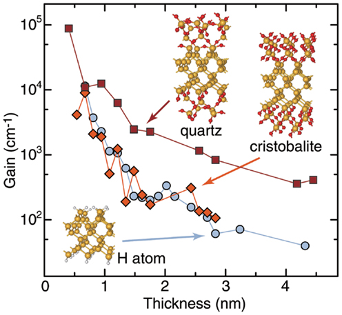
Figure 1. Optical gain of Si(001) thin films calculated from direct transitions across the energy gap only.
Experimentally, optical gain from the Si quantum dots (Pavesi et al., 2000) embedded in an insulating matrix (Pavesi et al., 2000; Nassiopoulou, 2004; Ossicini et al., 2006; Pavesi and Guillot, 2006) has been reported. It was confirmed that the interface states associated with oxygen atoms were important to explain the positive optical gain (Pavesi et al., 2000; Nassiopoulou, 2004; Ossicini et al., 2006; Pavesi and Guillot, 2006). It will be interesting to make these structures by top-down CMOS processes.
2.2. Theoretical Study of Light Emission from Germanium
Ge has two important differences from Si. One is that Ge has the minimum of the LCB at the L-point (L-valley), while Si has it near the X-point. The other is that Ge has a local minimum of the LCB at the Γ-point (Γ-valley), while Si does not. An L-valley is projected onto the Γ-point in the two-dimensional k-space for Ge(111) QW. For Ge(001) QW, no L-valley is projected onto the Γ-point. The small Γ-valley, which is not occupied unless a large number of electrons are injected, is always projected onto the Γ-point independently of the direction of the QW. While there are two approaches to obtain efficient light emission from Ge by direct transitions, using L-valleys of a Ge(111) QW or using the Γ-valley of bulk Ge, we think the latter is more promising. This is due to the fact that the calculated optical matrix element for the Γ-valley is very large compared to that for the L-valleys.
To enhance light emission from bulk Ge, applying tensile strain is known to be effective (Liu et al., 2010). Tensile strain makes the energy difference between the Γ and L-valleys small, and that makes electron injection into the Γ-valley easier. Also heavy n-type doping is known to be effective, because electrons can be injected into the Γ-valley if the L-valleys are already occupied by doped electrons.
In order to predict required strength of strain and amount of doping, we calculated optical gains of bulk Ge with and without strain. Figure 2 shows calculated optical gain as functions of injected electron density and hole densities. Here, the applied strain is assumed to be 0.25% biaxial tensile strain parallel to (001) surface and optical losses due to free carrier absorptions (Wang et al., 2013) are taken into account. This result shows that even bulk Ge without strain can have a positive optical gain, but number of electrons required for that is very large (1020 cm−3). Despite the relatively small amount of the strain (0.25%), the impact on the gain is clear. Owing to this enhancement, only half the electron density (5 × 1019 cm−3) is needed to have positive gain. In experiment, applying 0.25% strain is rather easy, and making higher strain will be possible, as we see in the following sections. Therefore, Ge lasers will be realized when an appropriate strain and carrier injection are achieved.
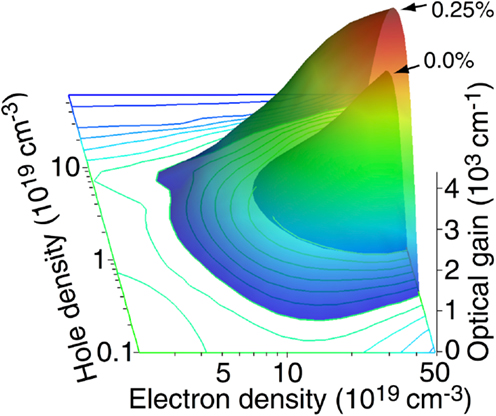
Figure 2. Optical gain of germanium as a function of injected electron density and hole density is shown. Those without strain and with 0.25% biaxial tensile strain parallel to (001) surface are shown.
3. Electro-Luminescence from Silicon Quantum-Well
As we reviewed in Section 1, it is well established that efficient recombination is observed in Si nanostructures by quantum confinement effects (Canham, 1990; Koshida and Koyama, 1992; Cullis et al., 1997; Ossicini et al., 2006; Daldosso and Pavesi, 2009). The nanostructures include quantum dots (Arakawa and Sakaki, 1982), nano-wires (Canham, 1990; Koshida and Koyama, 1992), quantum-well (QW) (Saito et al., 2006a,b, 2008, 2009; Saito, 2011), and fins (Saito et al., 2011a,b). One of the difficulties in developing an efficient light-emitting diode (LED) made of Si comes from the trade-off between quantum confinement and carrier injection. The surface of these Si nanostructures is easily oxidized to SiO2, and the band offsets between Si and SiO2 are too high to expect efficient current injection except for tunneling. In order to overcome this trade-off, lateral carrier injection into the Si QW was proposed (Saito et al., 2006a,b, 2008, 2009; Hoang et al., 2007; Noborisaka et al., 2011; Saito, 2011). As shown in Figures 3A–C, the Si QW LEDs were fabricated by local thinning of a silicon-on-insulator (SOI) substrate, and the Si QW was directly connected to the thick Si diffusion electrodes (Saito et al., 2006a,b). Both electrons and holes are laterally injected to the Si QW in these planar p-i-n diodes (Saito et al., 2006a,b, 2008, 2009; Noborisaka et al., 2011; Saito, 2011). Another advantage of these device structures is the fabrication of the Si QW through the LOCal-Oxidation of Si (LOCOS) process. The LOCOS process was originally developed for isolation of CMOS transistors (Sze and Lee, 2012; Taur and Ning, 2013). It was also used to evaluate the carrier mobility in the ultra-thin Si QW (Uchida and Takagi, 2003). Oxidation is one of the most precisely controlled processes in CMOS technologies, and we can routinely oxidize a large Si wafer (typically 8–10″ in diameter) within the local variation of <0.1 nm. Besides, the interface between Si and SiO2 is excellent with low interface trap density (<1011 cm−2) (Sze and Lee, 2012; Taur and Ning, 2013). The excellent interfacial quality and strong quantum confinement in Si nanostructures are critical to ensure high quantum efficiency (Gelloz et al., 2005). As shown in Figure 3E, EL is observed exclusively from the thin Si QW and EL from thick Si electrodes is negligible (Saito et al., 2006a). This supports the mechanism of EL based on quantum confinement (Ossicini et al., 2006; Suwa and Saito, 2009). The high carrier density in the thin Si QW also contributes to enhance the emissions (Saito et al., 2006a). By applying the back gate to the Si substrate, we can modulate the intensities of light emission, and the device can be called as an Si light-emitting transistor (Saito et al., 2006b).
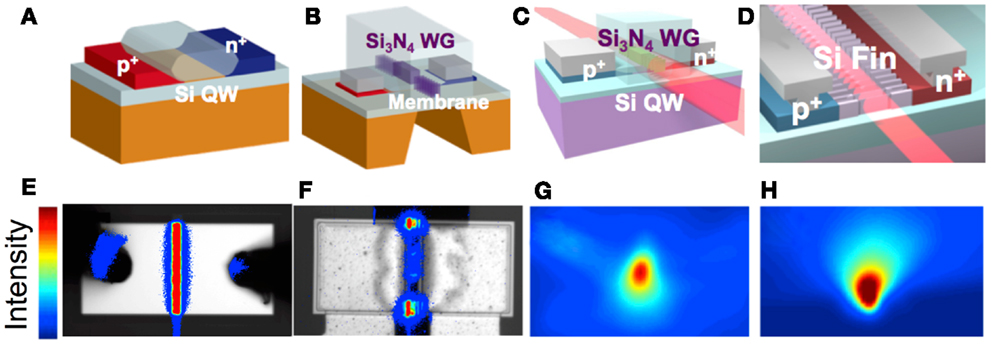
Figure 3. Development of an Si light source. (A) Si QW LED, (B) Si RCLED, (C) Si QW LED with thick BOX, (D) Si FinLED, and (E–H) EL images from these devices. (E,F) are plan views. (G,H) are near-field images at the edge of WG.
The next step toward the practical light source for Si photonics is to couple the light from Si to a cavity and a waveguide (WG). An Si-based WG cannot be used for emission from Si QW due to the absorption. An Si3N4 WG was fabricated on top of the Si QW by conventional lithography and dry etching (Saito et al., 2008, 2009). To enhance the optical confinement in the WG of the Si Resonant Cavity LED (RCLED), part of the supporting substrate was removed by using double sided aligner and anisotropic wet etching (Saito et al., 2008, 2009), as shown in Figure 3B. Evanescent coupling between the propagating optical mode and Si QW was expected, and the enhanced EL from the edge of the waveguide was observed (Figure 3F). More recently, SOI substrates with superior uniformities with thick Buried-OXide (BOX) (>2 μm) became available, and by using these wafers, strong optical confinement within the Si3N4 WG was ensured without removing the supporting Si substrate (Saito, 2011), as shown in Figure 3C. In fact, the near-field image of the propagating optical mode was taken at the edge of the WG (Figure 3G).
The obvious disadvantage of using the planar Si QW is the small confinement factor of the optical mode in the Si QW due to the thin single QW layer. It is not straightforward to make Si Multiple QWs (MQWs) (Fukatsu et al., 1992), if the surface of the Si QW is covered with the amorphous SiO2. As an alternative to the stacking of the Si MQWs, the Si FinLED has been proposed (Saito et al., 2011b), as shown in Figure 3D. Si fin is a vertical QW located perpendicular to an Si substrate, and it was proposed for a self-aligned double-gate CMOS field-effect-transistor, called a FinFET (Hisamoto et al., 2000). FinFETs are already used for mass production and more than one billion of FinFETs are integrated in the most recent MPU (INTEL, 20131; ITRS, 20122). Therefore, we can fabricate thousands of Si fins as MQWs at the same time simply by conventional photolithography and dry etching (Saito et al., 2011b). By applying forward bias to the Si FinLED, we can observe edge emission from the Si3N4 WG (Figure 3H). The EL spectra from the edge of the Si FinLED are shown in Figure 4A. The enhanced peaks from the edge of the stop band were observed due to the distributed-feedback structure of the periodic fins (Saito et al., 2011b). The non-linear increase of the EL intensity against the current is considered to come from stimulated emission (Figure 4B), but the estimated gain of <1 cm−1 was too low to overcome the threshold for a laser operation (Saito et al., 2011b).
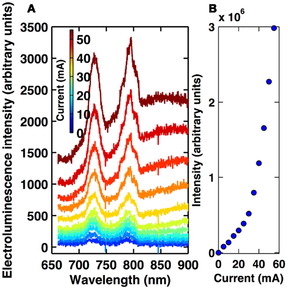
Figure 4. EL from Si FinLED taken from edge of WG. (A) Spectra and (B) integrated intensity.
4. Application of Photonic Nanostructures to Group IV Materials
4.1. Control of Light Emission by Photonic Crystals
The light emission properties of materials depend not only on material characteristics such as the dipole moment and the refractive index but also on the electromagnetic environment surrounding the material. In the previous sections, engineering group IV materials themselves such as quantum confinement, doping, and strain engineering have been discussed. Here, we discuss another approach, i.e., tailoring the electromagnetic environment by photonic nanostructures for improving light emission properties. The total efficiency of light-emitting devices can be expressed as a product of three factors: light emission efficiency ηemission, extraction efficiency ηextraction, and collection efficiency ηcollection. ηemission denotes how efficiently injected carriers recombine by emitting photons. ηextraction takes into account the fact that only a part of emitted photons can be extracted from the material. ηcollection expresses how much extracted photons can be collected by the first lens of the setup. All of them can be improved by photonic nanostructures. Photonic crystal (PhC) (Jannopoulos and Winn, 1995), which has a wavelength-scale periodic variation of refractive index, is an important photonic nanostructure for this application (see discussions in Iwamoto and Arakawa, 2012). Figure 5A shows a scanning electron microscope (SEM) image of a two-dimensional (2D) PhC slab, which is the most widely studied PhC structure. The structure can be fabricated by forming air holes in a thin semiconductor plate using conventional lithography and etching processes. In the structure, owing to the periodic modulation in refractive index, in-plane light propagation is governed by the photonic band structure. Strikingly, propagation is forbidden in photonic bandgaps (PBGs). Photonic band structures and PBGs can play roles to improve mainly ηextraction and ηcollection. Another important structure is the PhC nanocavity (Figure 5B), which is created by omitting air holes from the regular array. Photons are confined in in-plane and out-of-plane directions due to the PBG effect and total internal reflection, respectively. PhC nanocavities have a high quality factor Q and small mode volume Vc (~1 cubic wavelength or less). These two quantities are key parameters to enhance the spontaneous emission rate through the Purcell effect (Purcell, 1946) and improve ηemission. Particularly, for light emitters with broad linewidth such as bulk Si, Vc has a stronger impact (Ujihara, 1995). Such high-Q PhC nanocavities can uncover the quantum nature of light-matter interaction. Cavity quantum electrodynamics in a high-Q PhC nanocavity coupled with a single semiconductor quantum dot is a hot topic in the field (see, for example, Arakawa et al., 2012). Purcell enhancement factors of as large as 12 (Lo Savio et al., 2011) and 30 (Sumikura et al., 2014) were reported, which would be limited by the emission linewidth and the Q factor, respectively.
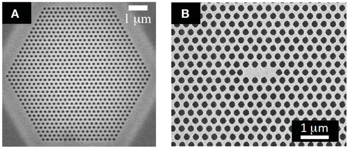
Figure 5. SEM images of a regular PhC structure with a triangular lattice (A) and a L3-type PhC nanocavity, in which three air holes along a Γ-K direction are omitted (B).
4.2. Enhanced Light Emission from Silicon Photonic Crystal Structures
PhC structures without cavities have been firstly applied to control the light emission from crystalline Si. In 2003, Zelsmann et al. (2003) reported enhanced PL extraction from a 2D PhC slab fabricated into the top Si layer of a SOI substrate at low temperature (Zelsmann et al., 2003). Similar enhancements at room temperature have been observed from arrays of Si nanoboxes (Cluzel et al., 2006a) and rods (Cluzel et al., 2006b) formed on SOI substrates. Strong light emission was observed at wavelengths corresponding to photonic band edges at the Γ point. Increasing the number of band edge within the emission spectrum of Si can lead to higher luminescence intensity. This is experimentally verified by increasing the lattice constant of PhC so that normalized frequencies corresponding to the Si emission wavelengths are increased (Fujita et al., 2008). Si light-emitting diodes (LEDs) with PhC patterns have also been demonstrated (Nakayama et al., 2010a; Iwamoto and Arakawa, 2012). The device schematically shown in Figure 6A was fabricated using a SOI substrate. Firstly, a lateral p-i-n junction was formed into the top 200-nm-thick Si layer by area-selective implantations of boron and phosphorous ions. Then, a PhC structure was patterned. To keep mechanical stability and better thermal conductivity, the buried-oxide (BOX) layer was not removed. An SEM image of the central part of a device is shown in Figure 6A. The i-region is 5 μm in length and 250 μm in width. EL spectra from devices with different PhC periods and from a device without PhC are shown in the inset of Figure 6B. EL emission increased as the period a increased. Figure 6B shows the integrated intensities from these devices as a function of injected current. The integrated intensity from the device with a = 750 nm is ~14 times stronger than that from an unpatterned LED. This enhancement is mainly caused by the improvement of ηextraction and ηcollection due to the photonic band structures as discussed above. ηemission is also expected to be enhanced in PhC nanocavities. Figure 7 shows room-temperature μ-PL spectra measured at the center of an L3-type PhC nanocavity compared to a non-patterned region (see the inset). The L3 PhC nanocavity was also fabricated into an SOI substrate. In this sample, the BOX layer was etched out in order to confine the photons strongly in the vertical direction. The PL intensity from the cavity was much larger than that from the non-patterned region. In addition, sharp peaks are observed only in the spectrum from the cavity. These peaks originate from the cavity resonant modes. For this particular sample with the air hole radius r = 0.37a, large enhancement of PL over 300 times was obtained for a cavity mode at 1,191 nm. As discussed in Section 1, this enhancement can be attributed to three factors. Detailed analysis including numerical simulation indicated that ηemission is improved by ~5 times (Iwamoto et al., 2007). The enhancement factors in ηemission ranging ~5−10 have been reported for Si interband transition (Fujita et al., 2008) and for light emission from optically active defects in Si (Lo Savio et al., 2011). The temperature dependence of cavity mode emission (Hauke et al., 2010; Lo Savio et al., 2011) and the dependence of PL on cavity mode volume Vc (Nakayama et al., 2012) suggest that the Purcell effect plays a role in this enhancement. The enhancement in ηemission reported so far is still too small for practical applications. However, this research would provide important insights for further development of light-emitting devices using group IV materials. Indeed, these pioneering works have stimulated theoretical investigations, which discuss the possibility of lasing oscillation in Si (Escalante and Martínez, 2012, 2013). Recent advances in this field are developments of Si LEDs with PhC nanocavities (Nakayama et al., 2011; Shakoor et al., 2013). Shakoor et al. (2013) recently reported Si LEDs using L3-type nanocavity structure, in which optically active defects created by hydrogen bombardment are used as light emission centers. They carefully designed the cavity structure to improving ηcollection and obtained sharp light emission at around 1.5 μm with a power density of 0.4 mW/cm2. The strain-induced dislocations (Ng et al., 2001; Kittler et al., 2013) will also be compatible to PhC nanocavities, since the emission energies are smaller than the band gap of Si. The combination of PhC nanocavities and defect engineering is very promising, and a wall plug efficiency of 0.7 × 10⁻⁸ was reported (Shakoor et al., 2013).
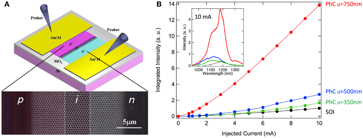
Figure 6. (A) Schematic representation of a silicon PhC LED is shown. The SEM image shows the center area of a device. (B) Integrated EL intensities for silicon PhC LED with various periods a and for an SOI LED with a flat surface. The inset shows corresponding EL spectra at 10 mA.
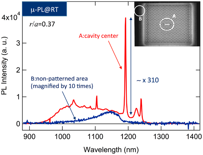
Figure 7. Room-temperature μ-PL spectra measured at the center of a PhC nanocavity and at a non-patterned area. The spectrum for the latter is magnified by ten times for better viewing.
4.3. Application of Photonic Crystal Structures to Other Emitters in Group IV Materials
Erbium ions have been investigated as one of the promising light emitters in Si. PhC nanocavities have been also applied to enhance the light emission from Er ions (Wang et al., 2012; Savio et al., 2013). Narrowing the cavity linewidth in Er-doped silicon nitride PhC nanocavities has been also demonstrated under optical pumping condition (Gong et al., 2010). As discussed in the previous sections, Ge is, at present, the most important material for future light-emitting devices in Si photonics. PhC (Nakayama et al., 2010b) and PhC nanocavities (Kurdi et al., 2008; Ngo et al., 2008) have been applied to increase the light emission from bulk Ge. Applying advanced strain/doping engineering technologies to photonic nanostructures would open a new route for boosting the light emission efficiency of Ge.
5. Generation of Tensile Strain in Ge Layers Epitaxially Grown on Si Substrate
In epitaxial growth of Ge on an Si substrate, a compressive strain in Ge, derived from the 4.2% lattice mismatch with Si, should be relaxed after growth beyond the critical thickness, while it has been reported by one of the authors that, during the cooling from the growth temperature to room temperature, a biaxial tensile strain as large as 0.2% is built-in due to the thermal expansion mismatch (Ishikawa et al., 2003, 2005; Cannon et al., 2004; Liu et al., 2005). It is known that the strain in semiconductors causes shifts in band edge energies, e.g., de Walle, 1989, modifying the gap energies, i.e., properties of optical transitions. The 0.2% tensile strain in Ge reduces the direct bandgap energy from 0.80 to ~0.77 eV, and as a result, the optical absorption edge (or the longer limit of detection wavelength) shifts from 1.55 to >1.60 μm, causing the increase of optical absorption coefficient at 1.55 μm (Ishikawa et al., 2003, 2005; Cannon et al., 2004; Liu et al., 2005). This property is effective for the detection of near-infrared (NIR) light used in the optical fiber communications (1.3–1.6 μm). A further attractive feature of the tensile strain in Ge is the reduction of energy difference in the conduction band between the direct Γ valley and indirect L-valley (e.g., Fischetti and Laux, 1996; Wada et al., 2006; Camacho-Aguilera et al., 2012; Nama et al., 2013; Süess et al., 2013). This feature stimulates researchers to obtain efficient NIR light emission from tensile-strained Ge due to the enhanced direct transition around the Γ point (e.g., Liu et al., 2007; Lim et al., 2009). In this section, the grown-in tensile strain in Ge on Si, generated due to the thermal expansion mismatch, is described. Figure 8A shows typical ω − 2θ x-ray diffraction (XRD) curves taken for 0.6-μm-thick Ge grown on a 525-μm-thick Si(001) substrate with the Cu Kα radiation as the x-ray source (0.15406 nm in wavelength). The samples were grown by ultrahigh-vacuum chemical vapor deposition with a source gas of GeH4 (9%) diluted in Ar. The growth temperature was 600°C, while a lower temperature of 370°C was used at the initial stage of Ge growth (~50 nm) in order to prevent the islanding, leading to Ge layers uniform in thickness (Luan et al., 1999; Ishikawa and Wada, 2010). After the growth, high-temperature annealing was carried out for one of the samples at 800°C for 20 min. Such annealing is often performed in order to reduce the threading-dislocation density (Luan et al., 1999). In our case, the density was reduced from 1 × 10⁹ to 1 − 2 × 108 cm−2. In Figure 8A, the peaks due to the (004) diffraction are clearly seen at around 2θ ~ 66° for both of the as-grown and annealed samples. It is important that the peaks were located at larger diffraction angles than that for unstrained Ge, indicating the reduction of out-of-plane lattice constant, i.e., the increase of in-plane lattice constant due to the generation of tensile strain. According to the peak positions, the in-plane biaxial tensile strain was estimated to be 0.11 and 0.22% for the as-grown and annealed samples, respectively.
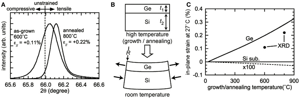
Figure 8. (A) ω − 2θ XRD curves for 0.6-μm-thick Ge on Si (001) substrate, (B) schematic illustration showing the generation of tensile stress/strain in Ge, and (C) theoretical curves and experimental data for biaxial tensile strain in Ge.
As mentioned above, such a tensile strain is generated in Ge due to the mismatch of thermal expansion coefficient with Si. As schematically shown in Figure 8B, the compressive strain in Ge due to the 4.2% lattice mismatch should be relaxed at the growth/annealing temperature, while the shrinkage in the Ge lattice during the cooling should be prevented by the thick Si substrate, since Si has a smaller thermal expansion coefficient than that of Ge. This means that a tensile (compressive) stress/strain is generated in Ge (Si), as in the bottom of Figure 8B. Taking into account the balance of forces together with the balance of moments in the stacked structure of Ge and Si, the tensile (compressive) strain in Ge (Si) is theoretically expressed as:
where, αi, Yi, ti, and zi represent the thermal expansion coefficient, the Young’s modulus, the layer thickness, and the location in the layer measured from the bottom of the layer for the i-th layer (1 for Ge and 2 for Si), respectively. The radius of curvature R is represented from
where TGR/AN and TRT represent the growth/annealing temperature before cooling and the room temperature (after the cooling), respectively. Since the first term is dominant in the right side of equation (1), the strains are almost independent of zi, the location within the layer. Therefore, equations (1) and (2) are simplified to:
The lines in Figure 8C represent the strains calculated for the Ge thickness of 0.6 μm and the Si thickness of 525 μm. Note that almost identical results can be obtained when the thickness of Si substrate t2 is much larger (more than ~100 times) than the Ge thickness t1. The parameters used in the calculation can be found in Ishikawa et al. (2005). It is found that a tensile strain on the order of 0.1% is generated in Ge at room temperature, while the compressive strain in Si is negligible. It is also found that higher growth/annealing temperature generates larger tensile strain after the cooling. These properties are qualitatively in good agreement with the XRD results in Figure 8A. However, quantitatively, the tensile strain observed by XRD was smaller than the theoretical one. This is probably ascribed to the residual compressive strain in Ge at the growth/annealing temperature (Ishikawa et al., 2005). From the viewpoint of optoelectronic integration of Ge devices on an Si platform, Si-on-insulator (SOI) wafers have been widely used. For Ge layers grown on SOI wafers, a similar amount of tensile strain should be generated, since the elastic deformation, derived from the thermal expansion mismatch, is governed by the thick Si substrate, rather than the buried SiO2 and the top Si layers with the thicknesses on the order of 1 μm or below. Patterning of the Ge layer as well as deposition of dielectric films embedding a strain could intentionally modify the strain in the Ge.
6. Direct Germanium Epitaxial Growth Process on Silicon
The Ge was epitaxially grown by using a cold-wall rapid thermal chemical vapor deposition system. Germane (GeH4) was used as a source gas, which was supplied with H2 carrier gas. As the starting point of improving the crystallinity and controlling the lattice strain, Ge layers with good surface morphology were grown at 420°C under relatively high pressure of 7,000 Pa. Then, the Ge layers were annealed in the same H2 atmosphere to improve the crystallinity. Figure 9 shows a reciprocal space map (RSM) of XRD (XRD-RSM) from the 130-nm-thick Ge layer directly grown on the Si substrate before and after H2 annealing. An intense Si (-1-13) peak was observed, which represented the diffraction from the Si substrate under the Ge layer. Since the XRD-RSM was measured by using semiconductor array detectors, errors in the counts occur if the diffraction intensity is very high; therefore, the streak line observed around the Si (-1-13) peak does not represent any actual diffraction. Since a Ge (-1-13) diffraction peak was observed from the Ge layer without annealing (Figure 9A), it could be confirmed that a single crystalline Ge layer was obtained by using low-temperature epitaxial growth. The displacement of the diffraction peak shows that the as-grown Ge layer still contained a compressive strain just after the low-temperature epitaxial growth at 420°C due to the larger lattice constant of Ge compared to that of the Si substrate. It has been reported that cyclic annealing at a relatively higher temperature can reduce the threading-dislocation density (Luan et al., 1999) in Ge layers. This has led to studies on the effect of annealing on the crystallinity and lattice strain of Ge layers. After low-temperature epitaxial growth of Ge layers at 420°C, the temperature was increased to the annealing temperature in the same H2 atmosphere as that during the epitaxial growth, and the Ge layers were then annealed at various temperatures for 10 min. XRD-RSMs of Ge layers annealed at a temperature (TGR/AN) of 700°C after the low-temperature epitaxial growth are shown in Figure 9B. The Ge (-1-13) diffraction peaks became much steeper and the peak intensity increased when the annealing temperature was increased, indicating that the crystallinity of the Ge layers was increased by the post-annealing.
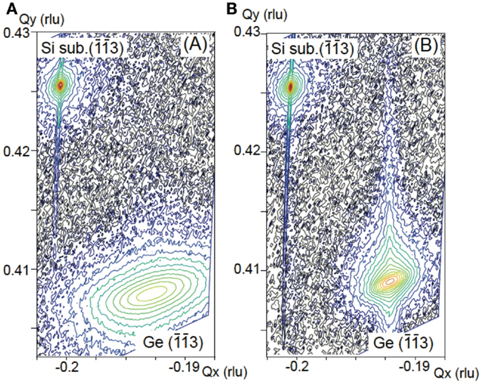
Figure 9. XRD-RSM of (-1-13) diffraction from Ge layer grown on Si substrate, (A) after low-temperature epitaxial growth and (B) after post-annealing.
The inset of Figure 10 shows the lattice strain in the Ge layers in the <001 > and <110 > crystal orientations as a function of the annealing temperature. We used standard Si wafers for this experiment, so that <001 > is perpendicular to the surface of the Ge film, while <110 > is in the plane of Ge film. The lattice strain in the <110 > crystal orientation increased as TGR/AN increased, and the strain in the <001 > crystal orientation showed an opposite dependence. Although the Ge layer contained a compressive strain in the <110 > crystal orientation at TGR/AN = 420°C, i.e., without annealing, this strain started decreasing when TGR/AN was increased, and the Ge was completely un-strainedat TGR/AN = 530°C. Furthermore, the sign of the lattice strain changed from compressive to tensile after annealing at TGR/AN > 530°C, and the tensile strain at TGR/AN = 700°C reached 0.19%. This result is consistent with previous studies (Cannon et al., 2004). Normally, a grown layer with a larger lattice constant compared to a substrate contains a compressive strain within the growth plane. However, since the Ge layers grown on the Si substrate were almost completely relaxed even after low-temperature growth, the Ge lattice could be dislocated at the Ge/Si interface by post-annealing, and the lattice strain of the Ge layer was relaxed during annealing at the relatively higher temperature with the volumes of Ge and Si determined by the thermal expansion coefficients (Singh, 1968; Okada and Tokumaru, 1984). After annealing, the volume of the Ge layer and the Si substrate both shrunk as the temperature decreased, and there was barely any change to the lattice alignment at low-temperature. The volume of the Si substrate returned to its original value because it was thick enough. However, the volume of the Ge layer could not return due to its larger thermal expansion coefficients. Therefore, the tensile lattice strain remained only in the Ge layers after cooling (Cerdeira et al., 1972). The ideal lattice strain in <110 > crystal orientation was also plotted in the inset of Figure 10, which was calculated with only the difference of the thermal expansion coefficients between Si and Ge, so these values indicate the maximum lattice strain. Since there are large discrepancies between calculation and measured values, it seems that relaxation ratio has a large effect on the lattice strain even at the lower temperatures. PL spectra from the post-annealed Ge layers with various annealing temperatures are shown in Figure 10. Although Ge is an indirect bandgap material and the L-valley has the lowest energy level in the conduction band, we were able to observe recombination between electrons and holes at the Γ-valley as luminescence at a wavelength of 1,550 nm, even from the bulk Ge (dashed line in Figure 10). A comparison with the post-annealed Ge layers shows that although the spectrum was very weak and broad for the as-grown Ge layer, an obvious peak could be observed from annealed samples at TGR/AN > 530°C. Moreover, the PL intensity increased and the peak shape became sharper as the annealing temperature was increased. The PL spectrum is strongly affected by crystallinity, because non-radiative recombination was significantly increased with defects such as dislocation and stacking faults. Therefore, these results suggest that the crystallinity of the Ge layers was improved by the post-annealing. The peak was observed at a shorter wavelength from the Ge layer annealed at 500°C compared with that from bulk Ge, and a red shift of the PL peaks occurred after post-annealing at a higher temperature. In addition, the peak wavelength from the unstrained Ge was 1,550 nm, which is almost the same value as that of the bulk Ge. These results show that the bandgap energy at the Γ-point was varied by the lattice strain in the Ge layers (Cerdeira et al., 1972; de Walle and Martin, 1986; de Walle, 1989), which is consistent with the XRD measurements. These results indicate that, in the range of this study, the most favorable PL characteristic can be obtained from the Ge layer after post-annealing at higher temperatures.
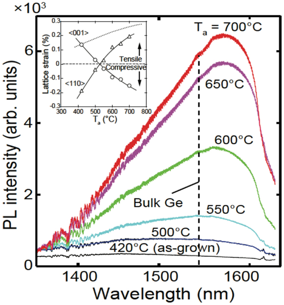
Figure 10. Photoluminescence spectra from Ge layers annealed with different temperatures are shown. Peak wavelength of photoluminescence from Ge layers red-shifted as annealing temperature increased, consistent with temperature induced tensile strain. Inset shows lattice strain of Ge layers grown on Si substrate along <001 > and <110 > crystal orientations as a function of annealing temperature. Dotted line indicates lattice strain calculated with difference between thermal expansion coefficients of Si and Ge.
7. Germanium Liquid-Phase Epitaxy and Devices for Photonic Application
Liquid-phase epitaxy (LPE) is a technique that was invented in the 1960s (Nelson, 1963) and developed in the 1970s (Wieder et al., 1977) for the fabrication of detectors, solar cells, LEDs (Saul and Roccasecca, 1973), and laser diodes (Panish et al., 1970). Originally used for III-V crystal growth, it has been adapted for SiGe-on-insulator (SGOI) and Ge-on-Insulator (GOI) growth by various groups (Liu et al., 2004; Tweet et al., 2005; Feng et al., 2008; Hashimoto et al., 2009; Miyao et al., 2009; Ohta et al., 2011) and is also referred to as rapid melt growth (RMG). The GOI technique was pioneered by Liu et al. (2004) for Ge-on-insulator fabrication. In this technique, a thin insulating layer is deposited on an Si substrate and patterned to open up seed windows. The target material, in this case Ge, is deposited using a non-selective method and patterned to form the desired features. This is then encapsulated using an insulating layer and heated up in a rapid-thermal-annealer (RTA) in order to melt the Ge. The micro-crucible holds the melt in place until the liquid epitaxial growth is complete. Upon cooling, liquid-phase epitaxial growth starts from the seed and propagates to the extremities of the strip structure. For the realization of single crystal Ge, epitaxial growth must proceed faster than unseeded random nucleation, so that the crystal regrowth starting from the seed is uninterrupted. Misfit dislocations arising at the SiGe interface in the seed area are necked down to the seed window as shown in Figure 11. The RMG is limited to the growth of structures of the order of around 3 μm in width and with a length of above 100 μm. The limitation is largely due to the surface tension of the insulator causing the Ge to form ball shapes while in the liquid phase.
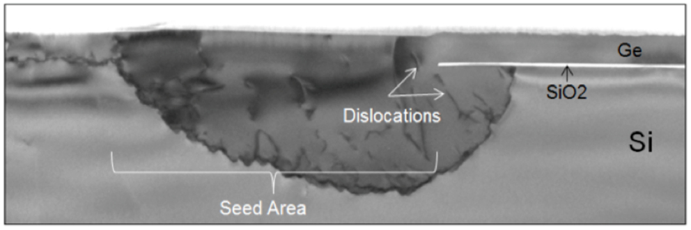
Figure 11. Transmission-electron-microscope (TEM) image of a high quality single crystalline Ge-on-insulator obtained using RMG. It can clearly be seen that the misfit dislocations from the lattice mismatch are confined to the seed region and that the crystalline Germanium lateral overgrowth is free from defects.
RMG is very attractive for the heterogeneous integration of Ge-based devices on insulator for electronics and photonics and has been demonstrated for Gate all around P-MOSFET (Feng et al., 2008), P-Channel FinFET (Feng et al., 2007), waveguide integrated Ge/Si heterojunction photodiodes (Tseng et al., 2013), or Ge Gate PhotoMOSFET (Going et al., 2014). These devices demonstrate the possibility of using RMG to obtain high quality Ge crystalline layers to create a bridge between electronic components and photonic components. This vision is clearly demonstrated by Going et al. (2014) in a Ge Gate PhotoMOSFET (Carroll et al., 2012) where a Ge-gated NMOS phototransistor is integrated on an Si photonics platform on SOI substrate. The resulting device, with 1-μm channel length, and 8-μm channel width, demonstrates a responsivity of over 18 A/W at 1550 nm with 583 nW of incident light. By increasing the incident power to 912 μW, the device operates at 2.5 GHz. Ge RMG or LPE on Si is therefore a promising technology for the fabrication of heterogeneous devices requiring high quality Ge layers such as MOSFETs, near-infrared detectors but also Ge-based lasers that are still to be demonstrated using this specific process technique. In fact, a highly tensile strain of 0.4% has successfully been applied to a Ge film grown by RMG process (Matsue et al., 2014), which is quite promising for light emission.
8. Time-Resolved Photoluminescence Study of Germanium on Silicon
The use of n-type tensile-strained Ge grown on Si substrates is one promising way to realize an efficient light source for Si photonics through the enhanced direct recombination from the Γ valley. However, the large lattice mismatch between Ge and Si inherently causes misfit dislocations at the interface, and threading dislocations during the growth. Besides, epitaxially grown Ge is usually a thin layer, so that both the interface and the surface become important. Therefore, investigation of the excess carrier lifetime is crucial for the realization of efficient light-emitting devices. Recently, the excess carrier dynamics of thin Ge film grown on either Si or SOI substrates have been investigated by time-resolved photoluminescence (Kako et al., 2012), microwave photoconductive decay (Sheng et al., 2013), and pump-probe transmission (Geiger et al., 2014) methods. Here, we present the time-resolved photoluminescence study of both non-doped and n-type Ge samples grown on Si.
The Ge samples were epitaxially grown on (100) Si substrates by using a cold-wall rapid thermal chemical vapor deposition system (Oda et al., 2014). There were two primary growth steps. The first step was the growth of an intrinsic Ge thin layer (≈100 nm) at low temperature followed by an annealing process. The second step was the regrowth of Ge on the first layer with another annealing process. In situ n-type doping was carried out during the second growth step by supplying phosphine. The Ge becomes biaxially strained (≈0.15%) due to the difference of the thermal expansion coefficients between Si and Ge. Time-resolved photoluminescence measurements were performed using a time-correlated single-photon counting method employing a superconducting single-photon detector (SSPD) with a time resolution of about 50 ps. A Ti:Sapphire pulsed laser was used as the excitation source (wavelength 710 nm, repetition rate 80 MHz, and pulse-duration 100 fs). The laser beam was focused on the sample surface using an objective lens. The photoluminescence from the samples was collected by the same objective and focused on to an optical fiber connected to the SSPD. Photoluminescence ranging from 1.2 to 1.8 μm was detected.
Figure 12A shows a time-resolved photoluminescence decay curve measured from a nominally undoped Ge sample (thickness 500 nm). In order to limit the effects of lateral diffusion, the laser spot size was set to ≈10 μm. The decay is a single exponential with a lifetime of 1 ns, which corresponds to the excess carrier lifetime of 2 ns. Germanium has an indirect bandgap, and as such, its excess carrier dynamics are determined by non-radiative recombination processes, such as Shockley-Read Hall (SRH) recombination and surface recombination processes. The photoluminescence decay lifetime, τPL, of undoped Ge is then related to the excess carrier lifetime, τex, as 2τPL = τex. The lifetime of excess carriers τex of an indirect semiconductor film depends on the thickness and can be represented by Sproul (1994) and Gaubas and Vanhellemont (2006) as:
where τB is the bulk lifetime, S is the surface recombination velocity, D is the ambipolar diffusion constant, and d is the layer thickness. The excess carrier lifetimes obtained for undoped Ge layers with different thicknesses (filled black circles) are shown in the inset of Figure 12A together with the black curve, which is a fit to the data using equation (6) with parameters of τB = 3.5 ns, S = 5.5 × 103 cm/s, and D = 30 cm2/s (The ambipolar diffusion constant Da could be estimated by changing the spot size and measuring the photoluminescence decay time). Both SRH bulk recombination and the surface recombination processes determine the excess carrier dynamics in our undoped Ge samples.
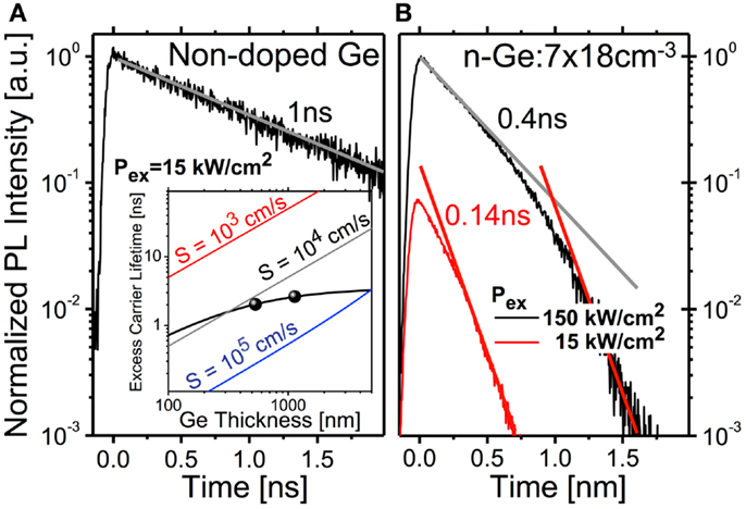
Figure 12. (A) Time-resolved PL curve for an undoped Ge sample. The inset shows the measured excess carrier lifetimes for two Ge thicknesses with simulated lifetimes using the equations shown in the text. (B) Time-resolved PL curves of an n-type sample for two excitation powers, 150 kW/cm2 (black line) and 15 kW/cm2 (red line).
Figure 12B shows time-resolved photoluminescence decay curves measured at two different excitation power densities from an n-type Ge sample (thickness 500 nm, doping concentration 7 × 1019 cm−3). The measured decay depends on both the excitation power density and time (in contrast to those measured from undoped samples, which are independent of the excitation power). The instantaneous lifetime (that measured at a particular point during the decay) depends on the photoluminescence intensity, and thus the excess carrier density. Based on the SRH non-radiative recombination model, the lifetime of excess carriers depends on their density (Linnros, 1998). This dependence can be simplified to τhl = τn + τp (τll = τp for n-type doping) in the two extreme conditions where the carrier density is high (low) when compared to the doping concentration (τn and τp are the inverse capture rates of the electrons and holes, respectively). The photoluminescence lifetime can be expressed as 2τPL = τhl (high excess carrier density) and τPL = τll (low excess carrier density). Therefore, from our measurements, we estimate τll = 0.14 ns, τhl = 0.8 ns based on SRH theory. The estimated τhl value is shorter than those found from the undoped samples. This difference might be attributed to an increased dislocation density introduced by the doping, but the estimation of τhl could be underestimation because the Auger process becomes important for doped samples (Gaubas and Vanhellemont, 2006). Further investigation is needed in order to obtain a better understanding.
9. Electro-Luminescence from Germanium
Realization of monolithic light sources compatible with the existing Si photonics platform is one of the most difficult challenges. Ge has attracted much attention as for possible future monolithic light sources owing to its emission wavelengths of ~1.6 μm suitable for an Si-based WG, in addition to the CMOS compatibility and the pseudo-direct band-gap character (Menéndez and Kouvetakis, 2004; Liu et al., 2007, 2012; Liang and Bowers, 2010; Michel et al., 2010; Boucaud et al., 2013; Liu, 2014). Recently, laser operation from Ge pumped optically (Liu et al., 2010) and electrically (Cheng et al., 2007; Camacho-Aguilera et al., 2012) has been reported. However, there is no report so far to reproduce their results. The optical gain from Ge is also achieved by the tensile-stress engineering (de Kersauson et al., 2011). The precise nature of the optical gain in Ge is still controversial (Carroll et al., 2012), but the high crystalline quality of Ge is one of the most critical factor to avoid non-radiative recombinations at dislocations. It is confirmed by several groups (Michel et al., 2010; Liu et al., 2012; Boucaud et al., 2013; Liu, 2014) that the primary challenges for engineering Ge as an active layer are: (i) crystallinity, (ii) high n-type doping, (iii) tensile strain, as confirmed theoretically (Suwa and Saito, 2010, 2011; Virgilio et al., 2013a,b). Here, we review some of the Ge light sources developed on SOI substrates.
9.1. Device Structure and Fabrication Process
As we discussed in section for Si light sources, lateral carrier injection is a natural choice for electrical pumping, since fabrication processes are based on planar CMOS technologies. We show several candidates for Ge light sources suitable for lateral carrier injection in Figure 13.
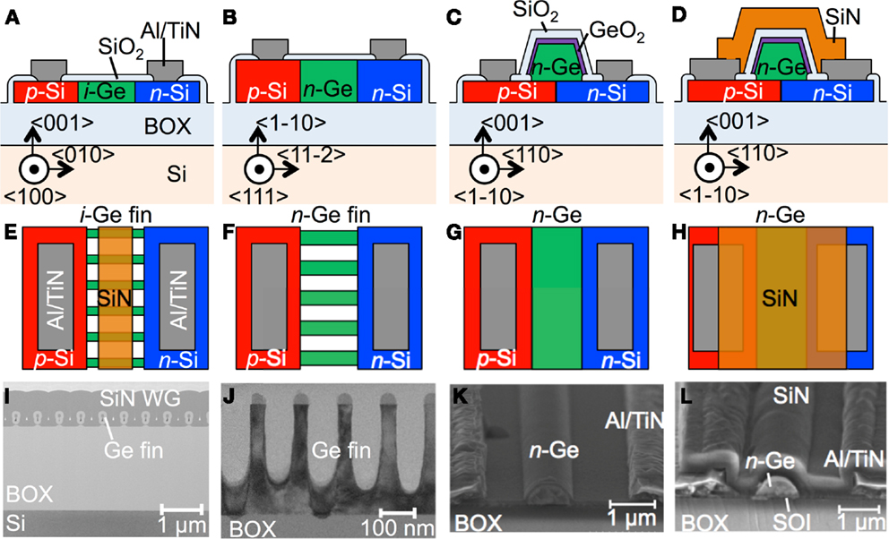
Figure 13. Development of a Ge light source. (A) i-Ge FinLED, (B) n-Ge FinLED, (C) n-Ge-WG-on-Si LED without SiN, and (D) n-Ge-WG-on-Si LED with SiN. (A–D) Cross section, (E–H) plan views, and (I–L) microscope images.
Figures 13A,E,I show schematic views and a transmission-electron-microscope (TEM) image of a Ge FinLED (Saito et al., 2011a), which uses Ge fins as MQWs embedded in Si3N4 WG. Ge fins were fabricated by the oxidation condensation technique (Tezuka et al., 2009) applied to SiGe fins (Saito et al., 2011a). Relatively, high crystallinity is expected in Ge fins, since the lattice mismatch between Si and Ge would be relaxed by stretching the fins during the oxidation (Saito et al., 2011a). In fact, the low dark current density of 1.86 × 10⁻⁵ A/cm−2 at a reverse bias of 1 − V and the strong breakdown current density of >1 MA/cm−2 were confirmed (Saito et al., 2011a).
In order to enhance the overlap between an optical mode and fins, Ge fins with (111) orientation at the sidewall were also developed (Tani et al., 2012), as shown in Figures 13B,F,J. To improve the patterning accuracy, Si (111) fins were fabricated by anisotropic wet etching, and n-Ge was re-grown after the condensation oxidation of SiGe fins (Tani et al., 2011).
Further increase of the coupling is realized by using a bulk Ge WG (Liu et al., 2007; Camacho-Aguilera et al., 2012; Tani et al., 2013a,b), as shown in Figures 13C,G,K for schematic views and the scanning electron microscope (SEM) image, rather than using Ge QW or Ge fins. The p- and n-type diffusion regions were formed in the 40 nm-thick SOI layer, and the Ge waveguide with 500-nm width and 500-μm length was directly grown on the SOI diode. The SOI thickness was designed to minimize the optical loss due to free carrier absorption in the diffusion electrodes. The Ge waveguide was doped with 1 × 1019 cm−3 of phosphorus, and the surface of the Ge waveguide was then passivated with GeO2 formed by low-temperature oxidation to reduce interfacial traps (Tani et al., 2012, 2013a). Then, metal electrodes were made on both diffusion regions.
To enhance light emission efficiency from Ge by tensile stress, several techniques have been developed, e.g., the use of the thermal expansion of relaxed Ge grown on Si (Ishikawa et al., 2003), the growth on buffer layers with larger lattice parameter (Huo et al., 2011), the mechanical deformation using membrane structures (Kurdi et al., 2010), the stress concentration in a membrane structure (Nama et al., 2013), and using external stressors (Ortolland et al., 2009; Ghrib et al., 2013). Considering the process compatibility to the lateral carrier injection, the Si3N4 film with the tensile stress of 250-MPa was employed (Tani et al., 2013a), as shown in Figures 13D,H,L.
9.2. Impact of Stress Engineering for Lateral Germanium on Silicon Diode
Figure 14A shows EL spectra of the Ge waveguide with 500-nm width and 500-μm length taken from the top of the substrate under continuous current injection of 60-mA. EL peak wavelength of the device with an SiN stressor is slightly longer than that without the SiN stressor due to the tensile strain-induced band-gap shrinkage, although the exact band-gap energy cannot be quantitatively estimated due to the additional peak shifts caused by heating under high currents. Moreover, as shown in Figure 14B, the peak intensity of the EL of the device with SiN stressor is 1.65 times larger than that without SiN stressors. Figure 14C shows two-dimensional stress mapping calculated by a finite element modeling of the Ge waveguide on the Si substrate covered by Si3N4 stressor. The tensile stress of 100 MPa is localized on the side wall of the Ge waveguide, while the in-plane compressive stress of 40 MPa exists on the top part of the Ge waveguide. The increase of the light emission efficiency was 22% caused by the tensile stress, after subtracting of the additional increase of 35% caused by the light extraction efficiency due to the reduced reflectance at the surface of the Ge waveguide by the 500 nm-thick Si3N4 layer (Tani et al., 2013a). Therefore, the stress engineering by Si3N4 is an appropriate option to improve the performance of Ge light sources. Recently, there are significant advances in stress engineering by manipulating free-standing Ge structures (Jain et al., 2012; Boztug et al., 2013; Süess et al., 2013; Sukhdeo et al., 2014), and enhanced direct recombination has been achieved.
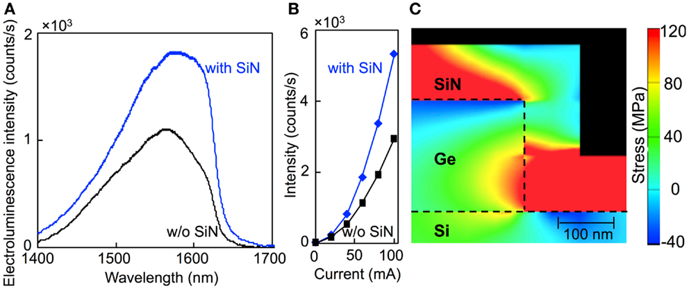
Figure 14. Strain engineering for n-Ge-WG-on-Si LED. (A) Spectra and (B) integrated intensity from experiments. (C) Stress mapping simulation.
10. Conclusion and Future Outlook
In this paper, we reviewed the recent progress on the developments of silicon and germanium light sources. There are many process options to fabricate silicon- and germanium-based nanostructures by using modern silicon technologies. For active materials, planar silicon single-quantum-well (Saito et al., 2006a,b, 2008, 2009; Hoang et al., 2007; Noborisaka et al., 2011; Saito, 2011) or multiple-quantum-wells made of silicon or germanium fins (Saito et al., 2011a,b) can be used. To enhance the recombination rates and the extraction efficiencies, photonic crystal structures have been introduced (Fujita et al., 2008; Nakayama et al., 2010a; Iwamoto and Arakawa, 2012). The further increase of the efficiency can be achieved by introducing tensile strain and n-type doping of the germanium (Ishikawa et al., 2003; Menéndez and Kouvetakis, 2004; Liu et al., 2007, 2012; Kurdi et al., 2010; Michel et al., 2010; Huo et al., 2011; Boucaud et al., 2013; Ghrib et al., 2013; Nama et al., 2013; Tani et al., 2013a; Liu, 2014).
Considering the success of the laser operation using the bulk germanium waveguides (Liu et al., 2010; Camacho-Aguilera et al., 2012), the next step will be to reduce the threshold current for pumping. It is critical to develop a process technology to fabricate a high crystalline quality germanium quantum-well compatible with the silicon photonics platform. If practical silicon or germanium laser diodes are available in the future, these group IV lasers will realize the convergence of electronics and photonics on a silicon chip.
Conflict of Interest Statement
The authors declare that the research was conducted in the absence of any commercial or financial relationships that could be construed as a potential conflict of interest.
Acknowledgments
We would like to thank research collaborators, engineers, and line managers in Hitachi, the University of Tokyo, and University of Southampton for supporting this project. We are also grateful to Prof. H. N. Rutt for his careful reading of the manuscript and constructive comments. Funding: parts of the studied discussed here was supported by Japan Society for the Promotion of Science (JSPS) through its “Funding Program for World-Leading Innovation R&D on Science and Technology (FIRST Program),” the Project for Developing Innovation Systems, and Kakenhi 216860312, MEXT, Japan. This work is also supported by EU, FP7, Marie-Curie, Carrier Integration Grant (CIG), PCIG13-GA-2013-618116, and University of Southampton, Zepler Institute, Research Collaboration Stimulus Fund.
Footnotes
References
Arakawa, Y., Iwamoto, S., Nomura, M., Tandaechanurat, A., and Ota, Y. (2012). Cavity quantum electrodynamics and lasing oscillation in single quantum dot-photonic crystal nanocavity coupled systems. IEEE J. Selec. Top. Quant. Elec. 18, 1818–1829. doi:10.1109/JSTQE.2012.2199088
Arakawa, Y., Nakamura, T., and Urino, Y. (2013). Silicon photonics for next generation system integration platform. Commun. Mag. IEEE 51, 72–77. doi:10.1109/MCOM.2013.6476868
Arakawa, Y., and Sakaki, H. (1982). Multidimensional quantum well laser and temperature dependence of its threshold current. Appl. Phys. Lett. 40, 939–941. doi:10.1063/1.92959
Boucaud, P., Kurdi, M. E., Ghrib, A., Prost, M., de Kersauson, M., Sauvage, S., et al. (2013). Recent advances in germanium emission. Photon. Res. 1, 102–109. doi:10.1364/PRJ.1.000102
Boztug, C., Sanchez-Perez, J. R., Yin, J., Lagally, M. G., and Paiella, R. (2013). Graiting-coupled mid-infrared light emission from tensile strained germanium nanomembranes. Appl. Phys. Lett. 103, 201114. doi:10.1002/smll.201201090
Camacho-Aguilera, R. E., Cai, Y., Patel, N., Bessette, J. T., Romagnoli, M., Kimerling, L. C., et al. (2012). An electrically pumped germanium laser. Opt. Express 20, 11316–11320. doi:10.1364/OE.20.011316
Canham, L. T. (1990). Silicon quantum wire array fabrication by electrochemical and chemical dissolution of wafers. Appl. Phys. Lett. 57, 1046–1048. doi:10.1063/1.103561
Cannon, D. D., Liu, J., Ishikawa, Y., Wada, K., Danielson, D. T., Jongthammanurak, S., et al. (2004). Tensile strained epitaxial Ge film on Si(100) substrate with potential application to L-band telecommunications. Appl. Phys. Lett. 84, 906. doi:10.1063/1.1645677
Carroll, L., Friedli, P., Neunschwander, S., Sigg, H., Cecchi, S., Isa, F., et al. (2012). Direct-gap gain and optical absorption in germanium correlated to the density of photoexcited carriers, doping, and strain. Phys. Rev. Lett. 109, 057402. doi:10.1103/PhysRevLett.109.057402
Cerdeira, F., Buchenauer, C. J., Pollak, F. H., and Cardona, M. (1972). Stress-induced shifts of first-order Raman frequencies of diamond- and zinc-blende-type semiconductors. Phys. Rev. B 5, 580–593. doi:10.1103/PhysRevB.5.580
Cheng, T. H., Kuo, P. S., Lee, C. T., Liao, M., Hung, T. A., and Liu, C. W. (2007). “Electrically pumped Ge laser at room temperature,” in IEEE Int. Conf. Electron Devices Meeting (IEDM), Washington, 659–662.
Cluzel, B., Pauc, N., Calvo, V., Charvolin, T., and Hadji, E. (2006a). Nanobox array for silicon-on-insulator luminescence enhancement at room temperature. Appl. Phys. Lett. 88, 133120. doi:10.1063/1.2191089
Cluzel, B., Calvo, V., Charvolin, T., Picard, E., Noé, P., and Hadji, E. (2006b). Single-mode room-temperature emission with a silicon rod lattice. Appl. Phys. Lett. 89, 201111. doi:10.1063/1.2364876
Cullis, A. G., Canham, L. T., and Calcott, P. D. J. (1997). The structural and luminescence properties of porous silicon. J. Appl. Phys. 82, 909–965. doi:10.1063/1.366536
Daldosso, N., and Pavesi, L. (2009). Nanosilicon photonics. Laser Photon. Rev. 3, 508–534. doi:10.1002/lpor.200810045
de Kersauson, M., Kurdi, M. E., David, S., Checoury, X., Fishman, G., Sauvage, S., et al. (2011). Optical gain in single tensile-strained germanium photonic wire. Opt. Express 19, 17925–17934. doi:10.1364/OE.19.017925
de Walle, C. G. V. (1989). Band lineups and deformation potentials in the model-solid theory. Phys. Rev. B 39, 1871. doi:10.1103/PhysRevB.39.1871
de Walle, C. G. V., and Martin, R. M. (1986). Theoretical calculations of heterojunction discontinuities in the Si/Ge system. Phys. Rev. B 34, 5621–5634. doi:10.1103/PhysRevB.34.5621
Deen, M. J., and Basu, P. K. (2012). Silicon Photonics Fundamentals and Devices. West Sussex: Wiley.
Escalante, J. M., and Martínez, A. (2012). Theoretical study about the gain in indirect bandgap semiconductor optical cavities. Physica B Condens. Matter 407, 2044–2049. doi:10.1016/j.physb.2012.02.002
Escalante, J. M., and Martínez, A. (2013). Optical gain by simultaneous photon and phonon confinement in indirect bandgap semiconductor acousto-optical cavities. Opt. Quant. Electron. 45, 1045–1056. doi:10.1007/s11082-013-9715-z
Evans, P., Fisher, M., Malendevich, R., James, A., Studenkov, P., Goldfarb, G., et al. (2011). “Multi-channel coherent PM-QPSK InP transmitter photonic integrated circuit (PIC) operating at 112 gb/s per wavelength,” in Optical Fiber Communication Conference (OFC) (Los Angeles: (IEEE) PDPC, OSA).
Fang, A. W., Park, H., Cohen, O., Jones, R., Paniccia, M. J., and Bowers, J. E. (2006). Electrically pumped hybrid AlGaInAs-silicon evanescent laser. Opt. Express 14, 9203–9210. doi:10.1364/OE.14.009203
Fathpour, S., and Jalali, B. (eds) (2012). Silicon Photonics for Telecommunications and Biomedicine. Boca Raton: CRC Press.
Feng, J., Thareja, G., Kobayashi, M., Chen, S., Poon, A., Bai, Y., et al. (2008). High-performance gate-all-around GeOI p-MOSFETs fabricated by rapid melt growth using plasma nitridation and ALD Al2O3 gate dielectric and self-aligned NiGe contacts. IEEE Electron Device Lett. 29, 805–807. doi:10.1109/LED.2008.2000613
Feng, J., Woo, R., Chen, S., Liu, Y., Griffin, P. B., and Plummer, J. D. (2007). P-channel germanium FinFET based on rapid melt growth. IEEE Electron Device Lett. 28, 637–639. doi:10.1109/LED.2007.899329
Fischetti, M. V., and Laux, S. E. (1996). Band structure, deformation potentials, and carrier mobility in strained Si, Ge, and SiGe alloys. J. Appl. Phys. 80, 2234. doi:10.1063/1.363052
Fujita, M., Tanaka, Y., and Noda, S. (2008). Light emission from silicon in photonic crystal nanocavity. IEEE J. Selec. Top. Quant. Elec. 14, 1090–1097. doi:10.1109/JSTQE.2008.918941
Fukatsu, S., Usami, N., Chinzei, T., Shiraki, Y., Nishida, A., and Nakagawa, K. (1992). Electroluminescence from strained SiGe/Si quantum well structures grown by solid source si molecular beam epitaxy. Jpn. J. Appl. Phys. 31, L1015–L1017. doi:10.1143/JJAP.31.L1015
Gaubas, E., and Vanhellemont, J. (2006). Dependence of carrier lifetime in germanium on resistivity and carrier injection level. Appl. Phys. Lett. 89, 142106. doi:10.1063/1.2358967
Geiger, R., Frigerio, J., Süess, M. J., Chrastina, D., Isella, G., Spolenak, R., et al. (2014). Excess carrier lifetimes in Ge layers on Si. Appl. Phys. Lett. 104, 062106. doi:10.1063/1.4865237
Gelloz, B., Kojima, A., and Koshida, N. (2005). Highly efficient and stable luminescence of nanocrystalline porous silicon treated by high-pressure water vapor annealing. Appl. Phys. Lett. 87, 031107. doi:10.1063/1.2001136
Gelloz, B., and Koshida, N. (2000). Electroluminescence with high and stable quantum efficiency and low threshold voltage from anodically oxidized thin porous silicon diode. J. Appl. Phys. 88, 4319–4324. doi:10.1063/1.1290458
Ghrib, A., Kurdi, M. E., de Kersauson, M., Prost, M., Sauvage, S., Checoury, X., et al. (2013). Tensile-strained germanium microdisks. Appl. Phys. Lett. 102, 221112. doi:10.1063/1.4809832
Going, R. W., Loo, J., Liu, T.-J. K., and Wu, M. C. (2014). Germanium gate PhotoMOSFET integrated to silicon photonics. IEEE J. Selec. Top. Quant. Elec. 20, 8201607. doi:10.1109/JSTQE.2013.2294470
Gong, Y., Makarova, M., Selçuk Yerci, R. L., Stevens, M. J., Baek, B., Nam, S. W., et al. (2010). Linewidth narrowing and Purcell enhancement in photonic crystal cavities on an Er-doped silicon nitride platform. Opt. Express 18, 2601–2612. doi:10.1364/OE.18.002601
Gunn, C. (2006). Cmos photonics for high-speed interconnects. Micro IEEE 26, 58–66. doi:10.1109/MM.2006.32
Hashimoto, T., Yoshimoto, C., Hosoi, T., Shimura, T., and Watanabe, H. (2009). Fabrication of local Ge-on-insulator structures by lateral liquid-phase epitaxy: effect of controlling interface energy between Ge and insulators on lateral epitaxial growth. Appl. Phys. Express 2, 066502. doi:10.1143/APEX.2.066502
Hauke, N., Zabel, T., Müller, K., Kaniber, M., Laucht, A., Bougeard, D., et al. (2010). Enhanced photoluminescence emission from two-dimensional silicon photonic crystal nanocavities. New J. Phys. 98, 053005. doi:10.1088/1367-2630/12/5/053005
Hisamoto, D., Lee, W., Kedzierski, J., Takeuchi, H., Asano, K., Kuo, C., et al. (2000). FinFET-a self-aligned double-gate MOSFET scalable to 20 nm. IEEE Trans. Electron Devices 47, 2320–2325. doi:10.1109/16.887014
Hoang, T., LeMinh, P., Holleman, J., and Schmitz, J. (2007). Strong efficiency improvement of SOI-LEDs through carrier confinement. IEEE Electron Device Lett. 28, 383–385. doi:10.1109/LED.2007.895415
Huo, Y., Lin, H., Chen, R., Makarova, M., Rong, Y., Li, M., et al. (2011). Strong enhancement of direct transition photoluminescence with highly tensile-strained Ge grown by molecular beam epitaxy. Appl. Phys. Lett. 98, 011111. doi:10.1063/1.3534785
Ishikawa, Y., and Wada, K. (2010). Germanium for silicon photonics. Thin Solid Films 518, S83–S87. doi:10.1016/j.tsf.2009.10.062
Ishikawa, Y., Wada, K., Cannon, D. D., Liu, J., Luan, H.-C., and Kimerling, L. C. (2003). Strain-induced band gap shrinkage in Ge grown on Si substrate. Appl. Phys. Lett. 82, 2044. doi:10.1063/1.1564868
Ishikawa, Y., Wada, K., Liu, J., Cannon, D. D., Luan, H.-C., Michel, J., et al. (2005). Strain-induced enhancement of near-infrared absorption in Ge epitaxial layers grown on Si substrate. J. Appl. Phys. 98, 013501. doi:10.1063/1.1943507
Iwamoto, S., and Arakawa, Y. (2012). Enhancement of light emission from silicon by utilizing photonic nanostructures. IEICE Trans. Electron E95-C, 206–212. doi:10.1587/transele.E95.C.206
Iwamoto, S., Arakawa, Y., and Gomyo, A. (2007). Observation of enhanced photoluminescence from silicon photonic crystal nanocavity at room temperature. Appl. Phys. Lett. 91, 211104. doi:10.1063/1.2816892
Jain, J. R., Hryciw, A., Baer, T. M., Miller, D. A. B., Brongersma, M. L., and Howe, R. T. (2012). A micromachining-based technology for enhancing germanium light-emission via tensile strain. Nat. Photonics 6, 398–405. doi:10.1038/nphoton.2012.111
Jannopoulos, J. D., and Winn, R. D. M. J. N. (1995). Photonic Crystals. Princeton, NJ: Princeton University Press.
Kageshima, H., and Shiraishi, K. (1997). Momentum-matrix-element calculation using pseudopotentials. Phys. Rev. B 56, 14985. doi:10.1103/PhysRevB.56.14985
Kako, S., Okumura, T., Oda, K., Suwa, Y., Saito, S., Ido, T., et al. (2012). “Time-resolved photoluminescence study of highly n-doped germanium grown on silicon,” in The 9th International Conference on Group IV Photonics (GFP), Vol. 7, San Diego, 340–342.
Kittler, M., Reiche, M., and Arguirov, T. (2013). “1.55 μm light emitter based on dislocation d1-emission in silicon,” in Microelectronics Technology and Devices (SBMicro), Symposium on IEEE, Curitiba.
Koshida, N., and Koyama, H. (1992). Visible electroluminescence from porous silicon. Appl. Phys. Lett. 60, 347–349. doi:10.1063/1.106652
Kurdi, M. E., Bertin, H., Martincic, E., de Kersauson, M., Fishman, G., Sauvage, S., et al. (2010). Control of direct band gap emission of bulk germanium by mechanical tensile strain. Appl. Phys. Lett. 96, 041909. doi:10.1063/1.3297883
Kurdi, M. E., Davida, S., Checourya, X., Fishmana, G., Boucauda, P., Kermarrecb, O., et al. (2008). Two-dimensional photonic crystals with pure germanium-on-insulator. Opt. Commun. 281, 846–850. doi:10.1016/j.optcom.2007.10.008
Laasonen, K., Pasquarello, A., Car, R., Lee, C., and Vanderbilt, D. (1993). Car-Parrinello molecular dynamics with Vanderbilt ultrasoft pseudopotentials. Phys. Rev. B 47, 10142. doi:10.1103/PhysRevB.47.10142
Liang, D., and Bowers, J. E. (2010). Recent progress in lasers on silicon recent progress in lasers on silicon recent progress in lasers on silicon recent progress in lasers on silicon. Nat. Photonics 4, 511–517. doi:10.1088/0034-4885/76/3/034501
Lim, P. H., Park, S., Ishikawa, Y., and Wada, K. (2009). Enhanced direct bandgap emission in germanium by micromechanical strain engineering. Opt. Express 17, 16358–16365. doi:10.1364/OE.17.016358
Linnros, J. (1998). Carrier lifetime measurements using free carrier absorption transients. I. Principle and injection dependence. J. Appl. Phys. 84, 275. doi:10.1063/1.368024
Liu, J. (2014). Monolithically integrated Ge-on-Si active photonics. Photonics 1, 162–197. doi:10.3390/photonics1030162
Liu, J., Camacho-Aguilera, R., Bessette, J. T., Sun, X., Wang, X., Cai, Y., et al. (2012). Ge-on-Si optoelectronics. Thin Solid Films 520, 3354–3360. doi:10.1016/j.tsf.2011.10.121
Liu, J., Cannon, D. D., Wada, K., Ishikawa, Y., Jongthammanurak, S., Danielson, D. T., et al. (2005). Tensile strained Ge p-i-n photodetectors on Si platform for C and L band telecommunications. Appl. Phys. Lett. 87, 011110. doi:10.1063/1.2037200
Liu, J., Sun, X., Camacho-Aguilera, R., Kimerling, L. C., and Michel, J. (2010). Ge-on-Si laser operating at room temperature. Opt. Lett. 35, 679–681. doi:10.1364/OL.35.000679
Liu, J., Sun, X., Pan, D., Wang, X., Kimerling, L. C., Koch, T. L., et al. (2007). Tensile-strained, n-type Ge as a gain medium for monolithic laser integration on Si. Opt. Express 15, 11272–11277. doi:10.1364/OE.15.011272
Liu, Y., Deal, M. D., and Plummer, J. D. (2004). High-quality single-crystal Ge on insulator by liquid-phase epitaxy on Si substrates. Appl. Phys. Lett. 84, 2563. doi:10.1063/1.1691175
Lo Savio, R., Portalupi, S. L., Gerace, D., Shakoor, A., Krauss, T. F., O’Faolain, L., et al. (2011). Room-temperature emission at telecom wavelengths from silicon photonic crystal nanocavities. Appl. Phys. Lett. 98, 201106. doi:10.1063/1.3591174
Luan, H.-C., Lim, D. R., Lee, K. K., Chen, K. M., Sandland, J. G., Wada, K., et al. (1999). High-quality Ge epilayers on Si with low threading-dislocation densities. Appl. Phys. Lett. 75, 2909. doi:10.1063/1.125187
Matsue, M., Yasutake, Y., Fukatsu, S., Hosoi, T., Shimura, T., and Watanabe, H. (2014). Strain-induced direct band gap shrinkage in local Ge-on-insulator structures fabricated by lateral liquid-phase epitaxy. Appl. Phys. Lett. 104, 031106. doi:10.1063/1.4862890
Menéndez, J., and Kouvetakis, J. (2004). Type-I Ge/Ge1− x− vSixSnv strained-layer heterostructure with a direct Ge bandgap. Appl. Phys. Lett. 85, 1175. doi:10.1063/1.1784032
Michel, J., Liu, J., and Kimerling, L. C. (2010). High-performance ge-on-si photodetectors. Nat. Photonics 4, 527–534. doi:10.1038/nphoton.2010.157
Michel, J., and Romagnoli, M. (2012). Germanium as the Unifying Material for Silicon Photonics. Bellingham: SPIE. doi:10.1117/2.1201206.004285
Miller, D. A. B. (2009). Device requirements for optical interconnections to silicon chips. Proc. IEEE 97, 1166–1185. doi:10.1109/JPROC.2009.2014298
Miyao, M., Tanaka, T., Toko, K., and Tanaka, M. (2009). Giant Ge-on-insulator formation by Si-Ge mixing-triggered liquid-phase epitaxy. Appl. Phys. Express 2, 045503. doi:10.1143/APEX.2.045503
Nakayama, S., Ishida, S., Iwamoto, S., and Arakawa, Y. (2012). Effect of cavity mode volume on photoluminescence from silicon photonic crystal nanocavities. Appl. Phys. Lett. 98, 171102.
Nakayama, S., Iwamoto, S., Ishida, S., and Arakawa, Y. (2010a). “Demonstration of a silicon photonic crystal slab led with efficient electroluminescence,” in International Conference on Solid State Devices and Materials (SSDM 2010) D-4-3, Tokyo.
Nakayama, S., Iwamoto, S., Ishida, S., Bordel, D., Augedre, E., Calvelier, L., et al. (2010b). Enhancement pf photoluminescence from germanium by utilizing air-bridge-type photonic crytsal slab. Physica E 42, 2556–2559. doi:10.1016/j.physe.2010.05.026
Nakayama, S., Iwamoto, S., Kako, S., Ishida, S., and Arakawa, Y. (2011). “Demonstration of silicon nanocavity led with enhanced luminescence,” in International Conference on Solid State Devices and Materials, Nagoya, I–8–2.
Nama, D., Sukhdeo, D. S., Kang, J.-H., Petykiewicz, J., Lee, J. H., Jung, W. S., et al. (2013). Strain-induced pseudoheterostructure nanowires confining carriers at room temperature with nanoscale-tunable band profiles. Nano Lett. 13, 3118–3123. doi:10.1021/nl401042n
Nassiopoulou, A. G. (2004). Silicon Nanocrystals in SiO2 Thin Layers, Vol. 9. Valencia: American Scientific Publishers, 793–813.
Nelson, H. (1963). Epitaxial growth from the liquid state and its application to the fabrication of tunnel and laser diodes. RCA Rev. 24, 603–615.
Ng, W. L., Lourenço, M. A., Gwilliam, R. M., Ledain, S., Shao, G., and Homewood, K. P. (2001). An efficient room-temperature silicon-based light-emitting diode. Nature 410, 192–194. doi:10.1038/35069092
Ngo, T.-P., Kurdi, M. E., Checoury, X., Boucaud, P., Damlencourt, J. F., Kermarrec, O., et al. (2008). Two-dimensional photonic crystals with germanium on insulator obtained by a condensation method. Appl. Phys. Lett. 93, 241112. doi:10.1063/1.3054332
Noborisaka, J., Nishiguchi, K., Ono, Y., Kageshima, K., and Fujiwara, A. (2011). Strong stark effect in electroluminescence from phosphorous-doped silicon-on-insulator metal-oxide-semiconductor field-effect transistors. Appl. Phys. Lett. 98, 033503. doi:10.1063/1.3543849
Oda, K., Tani, K., Saito, S.-I., and Ido, T. (2014). Improvement of crystallinity by post-annealing and regrowth of Ge layers on Si substrates. Thin Solid Films 550, 509–514. doi:10.1016/j.tsf.2013.10.136
Ohta, Y., Tanaka, T., Toko, K., Sadoh, T., and Miyao, M. (2011). Growth-direction-dependent characteristics of Ge-on-insulator by Si-Ge mixing triggered melting growth. Solid State Electron. 60, 18–21. doi:10.1016/j.sse.2011.01.039
Okada, Y., and Tokumaru, Y. (1984). Precise determination of lattice parameter and thermal expansion coefficient of silicon between 300 and 1500 K. J. Appl. Phys. 56, 314. doi:10.1063/1.333965
Ortolland, C., Okuno, Y., Veheyen, P., Kerner, C., Stapelmann, C., Aoulaiche, M., et al. (2009). Stress memorization technique-fundamental understanding and low-cost integration for advanced CMOS technology using a nonselective process. IEEE Trans. Electron Devices 56, 1690–1697. doi:10.1109/TED.2009.2024021
Ossicini, S., Pavesi, L., and Priolo, F. (2006). Light Emitting Silicon for Microphotonics. Berlin: Springer.
Panish, M. B., Hayashi, I., and Sumski, S. (1970). Double heterostructure injection lasers with room temperature thresholds as low as 2300 a/cm2. Appl. Phys. Lett. 16, 326. doi:10.1063/1.1653213
Pavesi, L., and Guillot, G. (eds) (2006). Optical Interconnects The Silicon Approach. Berlin: Springer.
Pavesi, L., Negro, L. D., Mazzoleni, C., Franzò, G., and Priolo, F. (2000). Optical gain in silicon nanocrystals. Nature 408, 440–444.
Perdew, J. P., Burke, K., and Wang, Y. (1996). Generalized gradient approximation for the exchange-correlation hole of a many-electron system. Phys. Rev. B 54, 16533. doi:10.1103/PhysRevB.54.16533
Rylyakov, A., Schow, C., Lee, B., Green, W., Campenhout, J. V., Yang, M., et al. (2011). “A 3.9ns 8.9mW 4×4 silicon photonic switch hybrid integrated with CMOS driver,” in Int. Solid-State Circuits Conference (ISSCC) (San Francisco: IEEE), 222–224.
Saito, S. (2011). “Silicon and germanium quantum well light-emitting diode,” in IEEE 8th Int. Conf. Group IV Photonics, London, 166–168.
Saito, S., Hisamoto, D., Shimizu, H., Hamamura, H., Tsuchiya, R., Matsui, Y., et al. (2006a). Electro-luminescence from ultra-thin silicon. Jpn. J. Appl. Phys. 45, L679–L682. doi:10.1143/JJAP.45.L679
Saito, S., Hisamoto, D., Shimizu, H., Hamamura, H., Tsuchiya, R., Matsui, Y., et al. (2006b). Silicon light-emitting transistor for on-chip optical interconnection. Appl. Phys. Lett. 89, 163504. doi:10.1063/1.2360783
Saito, S., Oda, K., Takahama, T., Tani, K., and Mine, T. (2011a). Germanium fin light-emitting diode. Appl. Phys. Lett. 99, 241105. doi:10.1364/OE.22.005927
Saito, S., Takahama, T., Tani, K., Takahashi, M., Mine, T., Suwa, Y., et al. (2011b). Stimulated emission of near-infrared radiation in silicon fin light-emitting diode. Appl. Phys. Lett. 98, 261104. doi:10.1063/1.3605255
Saito, S., Sakuma, N., Suwa, Y., Arimoto, H., Hisamoto, D., Uchiyama, H., et al. (2008). “Observation of optical gain in ultra-thin silicon resonant cavity light-emitting diode,” in IEEE Int. Conf. Electron Devices Meeting (IEDM), San Francisco, 19.5.
Saito, S., Suwa, Y., Arimoto, H., Sakuma, N., Hisamoto, D., Uchiyama, H., et al. (2009). Stimulated emission of near-infrared radiation by current injection into silicon (100) quantum well. Appl. Phys. Lett. 95, 241101. doi:10.1063/1.3273367
Saul, R. H., and Roccasecca, D. D. (1973). Vapor-doped multislice LPE for efficient GaP green LED’s. J. Electrochem. Soc. 120, 1128–1131. doi:10.1149/1.2403644
Savio, R. L., Miritello, M., Shakoor, A., Cardile, P., Welna, K., Andreani, L. C., et al. (2013). Enhanced 1.54 μm emission in Y-Er disilicate thin films on silicon photonic crystal cavities. Opt. Express 21, 10278–10288. doi:10.1364/OE.21.010278
Shakoor, A., Lo Savio, R., Cardile, P., Portalupi, S. L., Gerace, D., Welna, K., et al. (2013). Room temperature all-silicon photonic crystal nanocavity light emitting diode at sub-bandgap wavelengths. Laser Photon. Rev. 7, 114–121. doi:10.1002/lpor.201200043
Sheng, J. J., Leonhardt, D., Han, S. M., Johnston, S. W., Cederberg, J. G., and Carroll, M. S. (2013). Empirical correlation for minority carrier lifetime to defect density profile in germanium on silicon grown by nanoscale interfacial engineering. J. Vac. Sci. Technol. B Microelectron. 31, 051201. doi:10.1116/1.4816488
Singh, H. P. (1968). Determination of thermal expansion of germanium, rhodium and iridium by x-rays. Acta Crystallogr. A 24, 469–471. doi:10.1107/S056773946800094X
Sproul, A. B. (1994). Dimensionless solution of the equation describing the effect of surface recombination on carrier decay in semiconductors. J. Appl. Phys. 76, 2851. doi:10.1063/1.357521
Steger, M., Yang, A., Sekiguchi, T., Saeedi, K., Thewalt, M. L. W., Henry, M. O., et al. (2011). Photoluminescence of deep defects involving transition metals i Si: new insights from highly enriched 28Si. J. Appl. Phys. 110, 081301. doi:10.1063/1.3651774
Süess, M. J., Geiger, R., Minamisawa, R. A., Schiefler, G., Frigerio, J., Chrastina, D., et al. (2013). Analysis of enhanced light emission from highly strained germanium microbridges. Nat. Photonics 7, 466–472. doi:10.1038/nphoton.2013.67
Sukhdeo, D. S., Nam, D., Kang, J. H., Brongersma, M. L., and Saraswat, K. C. (2014). Direct bandgap germanium-on-silicon inferred from 5.7% <100 > uniaxial tensile strain. Photon. Res. 2, A8–A13. doi:10.1364/PRJ.2.0000A8
Sumikura, H., Kuramochi, E., Taniyama, H., and Notomi, M. (2014). Ultrafast spontaneous emission of copper-doped silicon enhanced by an optical nanocavity. Sci. Rep. 4, 5040. doi:10.1038/srep05040
Suwa, Y., and Saito, S. (2009). Intrinsic optical gain of ultrathin silicon quantum wells from first-principles calculations. Phys. Rev. B 79, 233308. doi:10.1103/PhysRevB.79.233308
Suwa, Y., and Saito, S. (2010). “First-principles study of light emisson from germanium guantum-well,” in IEEE 22nd Int. Semiconductor Laser Conference (ISLC), Kyoto, 131–132.
Suwa, Y., and Saito, S. (2011). “First-principles study of light emission from silicon and germanium due to direct transitions,” in IEEE 8th Int. Conf. Group IV Photonics, London, 222–224.
Sze, S. M., and Lee, M. K. (2012). Semiconductor Devices: Physics and Technology, 3rd Edn. Singapore: John Wiley and Sons.
Tani, K., Oda, K., Kasai, J., Okumura, T., Mine, T., Saito, S., et al. (2013a). “Germanium waveguides on lateral silicon-on-insulator diodes for monolithic light emitters and photo detectors,” in Group IV Photonics (GFP), IEEE 10th International Conference (Seoul: IEEE), 134–135.
Tani, K., Oda, K., Okumura, T., Takezaki, T., Kasai, J., Mine, T., et al. (2013b). “Enhanced electroluminescence from germanium waveguides by local tensile strain with silicon nitride stressors,” in International Conference on Solid State Devices and Materials (SSDM) (Fukuoka: SSDM), K–6–3.
Tani, K., Saito, S., Oda, K., Miura, M., Mine, T., Sugawara, T., et al. (2011). “Ge(111)-fin light-emitting diodes,” in IEEE 8th Int. Conf. Group IV Photonics, London, 217–219.
Tani, K., Saito, S., Oda, S., Okumura, T., Mine, T., and Ido, T. (2012). “Lateral carrier injection to germanium for monolithic light sources,” in Group IV Photonics (GFP), IEEE 9th Int. Conf, San Diego, 328–330.
Taur, Y., and Ning, T. H. (2013). Fundamentals of Modern VLSI Devices, 2nd Edn. Cambridge: Cambridge University Press.
Tezuka, T., Toyoda, E., Irisawa, T., Hirashita, N., Moriyama, Y., Sugiyama, N., et al. (2009). Structural analyses of strained SiGe wires formed by hydrogen thermal etching and Ge-condensation processes. Appl. Phys. Lett. 94, 081910. doi:10.1063/1.3086884
Tseng, C.-K., Chen, W.-T., Chen, K.-H., Liu, H.-D., Kang, Y., Na, N., et al. (2013). A self-assembled microbonded germanium/silicon heterojunction photodiode for 25 Gb/s high-speed optical interconnects. Sci. Rep. 3, 3225. doi:10.1038/srep03225
Tweet, D. J., Lee, J. J., Maa, J.-S., and Hsu, S. T. (2005). Characterization and reduction of twist in Ge on insulator produced by localized liquid phase epitaxy. Appl. Phys. Lett. 87, 141908. doi:10.1063/1.2077860
Uchida, K., and Takagi, S. (2003). Carrier scattering induced by thickness fluctuation of silicon-on-insulator film in ultrathin-body metal–oxide–semiconductor field-effect transistors. Appl. Phys. Lett. 82, 2916. doi:10.1063/1.1571227
Ujihara, K. (1995). “Effects of atomic broadening on spontaneous emission in an optical microcavity,” in Spontaneous Emission and Laser Oscillation in Microcavities, eds H. Yokoyama and K. Ujihara (Boca Raton, FL: CRC Press), 81–107.
Urino, Y., Horikawa, T., Nakamura, T., and Arakawa, Y. (2013). “High density optical interconnects integrated with lasers, optical modulators and photodetectors on a single silicon chip,” in Optical Fiber Communication Conference (OFC), (Anaheim: OSA), OM2J.
Vanderbilt, D. (1990). Soft self-consistent pseudopotentials in a generalized eigenvalue formalism. Phys. Rev. B 41, 7892(R). doi:10.1103/PhysRevB.41.7892
Virgilio, M., Manganelli, C. L., Grosso, G., Pizzi, G., and Capellini, G. (2013a). Radiative recombination and optical gain spectra in biaxially strained n-type germanium. Phys. Rev. B 87, 235313. doi:10.1103/PhysRevB.87.235313
Virgilio, M., Manganelli, C. L., Grosso, G., Schroeder, T., and Capellini, G. (2013b). Photoluminescence, recombination rate, and gain spectra in optically excited n-type and tensile strained germanium layers. J. Appl. Phys. 114, 243102. doi:10.1063/1.4849855
Wada, K., Liu, J., Jongthammanurak, S., Cannon, D. D., Danielson, D. T., Ahn, D., et al. (2006). Si Microphotonics for Optical Interconnection. Berlin: Springer Verlag.
Wale, M. (2008). “Photonic integration – an industrial perspective,” in European Photonic Integration Forum (Brussels: European Photonics Integration Forum).
Wang, X., Li, H., Camacho-Aguilera, R., Cai, Y., Kimerling, L. C., Michel, J., et al. (2013). Infrared absorption of n-type tensile-strained Ge-on-Si. Opt. Lett. 38, 652–654. doi:10.1364/OL.38.000652
Wang, Y., Zhang, J., Wu, Y., An, J., Li, J., Wang, H., et al. (2012). Light emission enhancement from Er-doped silicon photonic crystal double-heterostructure microcavity. IEEE Photon. Technol. Lett. 24, 1041–1135. doi:10.1109/LPT.2011.2173183
Wieder, H. H., Clawson, A. R., and McWilliams, G. E. (1977). InxGa1− xAsvP1− v/InP heterojunction photodiodes. Appl. Phys. Lett. 31, 468. doi:10.1063/1.89718
Keywords: silicon, photonics, CMOS, germanium, epitaxy, luminescence, quantum, strain
Citation: Saito S, Gardes FY, Al-Attili AZ, Tani K, Oda K, Suwa Y, Ido T, Ishikawa Y, Kako S, Iwamoto S and Arakawa Y (2014) Group IV light sources to enable the convergence of photonics and electronics. Front. Mater. 1:15. doi: 10.3389/fmats.2014.00015
Received: 12 June 2014; Paper pending published: 28 July 2014;
Accepted: 29 August 2014; Published online: 17 September 2014.
Edited by:
Jifeng Liu, Dartmouth College, USAReviewed by:
Androula Galiouna Nassiopoulou, National Centre for Scientific Research Demokritos, GreeceRaul J. Martin-Palma, Universidad Autonoma de Madrid, Spain
Jifeng Liu, Dartmouth College, USA
Copyright: © 2014 Saito, Gardes, Al-Attili, Tani, Oda, Suwa, Ido, Ishikawa, Kako, Iwamoto and Arakawa. This is an open-access article distributed under the terms of the Creative Commons Attribution License (CC BY). The use, distribution or reproduction in other forums is permitted, provided the original author(s) or licensor are credited and that the original publication in this journal is cited, in accordance with accepted academic practice. No use, distribution or reproduction is permitted which does not comply with these terms.
*Correspondence: Shinichi Saito, Nano Research Group, Electronics and Computer Science, Faculty of Physical Sciences and Engineering, Highfield Campus, University of Southampton, Southampton SO17 1BJ, UK e-mail: s.saito@soton.ac.uk