Elucidating the Exceptional Passivation Effect of 0.8 nm Evaporated Aluminium on Transparent Copper Films
 Philip Bellchambers
 Jaemin Lee1
  Silvia Varagnolo
 Marc Walker
 Ross A. Hatton
- 1Department of Chemistry, University of Warwick, Coventry, United Kingdom
- 2Department of Physics, University of Warwick, Coventry, United Kingdom
Slab-like copper films with a thickness of 9 nm (~70 atoms) and sheet resistance of ≤ 9 Ω sq−1 are shown to exhibit remarkable long-term stability toward air-oxidation when passivated with an 0. 8 nm aluminium layer deposited by simple thermal evaporation. The sheet resistance of 9 nm Cu films passivated in this way, and lithographically patterned with a dense array of ~6 million apertures per cm2, increases by < 3.5% after 7,000 h exposure to ambient air. Using a combination of annular-dark field scanning transmission electron microscopy, nanoscale spatially resolved elemental analysis and atomic force microscopy, we show that this surprising effectiveness of this layer results from spontaneous segregation of the aluminium to grain boundaries in the copper film where it forms a ternary oxide plug at those sites in the metal film most vulnerable to oxidation. Crucially, the heterogeneous distribution of this passivating oxide layer combined with its very low thickness ensures that the underlying metal is not electrically isolated, and so this simple passivation step renders Cu films stable enough to compete with Ag as the base metal for transparent electrode applications in emerging optoelectronic devices.
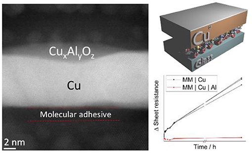
Graphical Abstract. (Left) Cross-sectional image of a 9 nm Cu film passivated by 0.8 nm Al as illustrated (Top-Right) which imparts dramatically improved stability in air (Bottom-Right).
Introduction
It is now widely recognized that alternatives to conventional conducting oxide window electrode materials, such as tin doped indium oxide and fluorine doped tin oxide, are required to enable optoelectronic devices compatible with flexible substrates and low cost roll-to-roll manufacturing (Ghosh, 2013; Yun, 2017). Unpatterned optically thin metal film electrodes are now emerging as a viable challenger because they are compatible with flexible substrates and roll-to-roll processing, whilst also offering the important advantages over metal nanowire electrodes of much lower surface roughness and superior stability toward electromigration (Stec and Hatton, 2012; Griffith et al., 2016; Sannicolo et al., 2016; Lu H. et al., 2018). On plastic substrates lithographic patterning of thin metal film electrodes and/or the use of wide band gap anti-reflecting interlayers enables performance competitive with high performance conducting oxide electrodes (Kim et al., 2001; Sahu and Huang, 2006; Sivaramakrishnan and Alford, 2009; Gao et al., 2014; Kang et al., 2015; Zilberberg and Riedl, 2016; Yun, 2017). Vacuum evaporation is also well-established as a low cost production method for thin metal films over large areas, most notably for the packaging industry, and so is particularly attractive as a low cost path to large scale deposition of optically thin metal films (Mulligan et al., 2013; Griffith et al., 2016).
Due to the high electrical conductivity and low optical loses, Ag is currently the metal of choice for metal window electrode applications (Griffith et al., 2016), although it is recognized that its high cost may necessitate recycling if it is to be used in low cost applications such as organic photovoltaics (OPVs) (Krebs et al., 2014). Ag films are also sensitive to oxidation in ambient air, a process which is detrimental to their performance as electrodes in devices (Watanabe et al., 2007; Kim et al., 2009; Behrendt et al., 2015). Zhang et al. (2014) have shown that alloying Ag with ~10% aluminium by co-sputtering is a very effective approach for stabilizing optically thin Ag films without compromising the optical properties, although the sheet resistance of Al doped Ag electrodes is not as low as can be achieved with pure Ag. In general, literature reports pertaining to the long-term stability of optically thin Ag films toward oxidation in air are sparse (Ellmer, 2012; Behrendt et al., 2015; Yun, 2017; Lu H. et al., 2018), which is surprising given the potential technological importance. The substrate electrode is very often manipulated in air prior to integration into a device, and it is well-understood that the gradual ingress of air into flexible electronic devices is inevitable due to the limited barrier properties of transparent encapsulants compatible with flexible substrates (Dennler et al., 2006; Lu M. et al., 2018), so the long-term stability toward air-oxidation is an important consideration for many applications.
Copper (Cu) is an attractive alternative to Ag for use as a window electrode for cost sensitive applications such as OPVs because it has a conductivity comparable to Ag at ~1% of the cost (Matula, 1979)1. The higher optical losses in Cu for wavelengths below 500 nm can be mitigated by electrode and/or device design, including using a metal oxide overlayer to increase transparency (Hutter and Hatton, 2015; Zhao et al., 2016; Pereira et al., 2018). However, the application of Cu window electrodes has so far been limited, due to the higher susceptibility of Cu toward oxidation in air which results in the formation of a mixture of the short-lived hydroxide (Cu(OH)2), Cu2O, and CuO (Gattinoni and Michaelides, 2015). Notably, some crystal faces of Cu are far more resistant to oxidation than others, although the order of reactivity and mechanism is debated (Young et al., 1956; Li et al., 1991; Wiame et al., 2007; Platzman et al., 2008). In contrast to the native oxide layer at the surface of aluminium (Al) the process of Cu oxidation in air is not self-limiting (Li et al., 1991; O'Reilly et al., 1995; Gao et al., 2001; Platzman et al., 2008; Biesinger et al., 2010), although Cu2O and CuO do not necessarily electrically isolate the metal since both are p-type semiconductors with accessible valance bands for hole conduction (Mugwang'a et al., 2013). In the context of very thin Cu films suitable for window electrode applications, surface oxidation does however have the detrimental effect of increasing the electrode sheet resistance due to the significant reduction in metal thickness, and so it is important to limit surface oxidation as far as possible (Hsu et al., 2012; Chen et al., 2014; Lee et al., 2015; Stewart et al., 2015).
One approach for the passivation of Cu films that has proved remarkably effective is the use of a sub-1 nm Al layer deposited by simple vacuum evaporation (Gan et al., 2002; Hutter et al., 2013; Tyler et al., 2015). Hutter et al. (2013) have shown there is no increase in the sheet resistance of a 7 nm thick Cu film after 120 h in ambient air when capped with 0.8 nm Al. In that work it was postulated that a compact ternary oxide layer of aluminium-copper-oxide caps the entire surface of the Cu film, since both Cu and Al oxide fragments were observed using secondary ion mass spectroscopy. It is however remarkable that such a thin oxide layer is so effective given that the native oxide on both Al and Cu exceeds 2 nm in thickness (Chawla et al., 1992; Platzman et al., 2008; Evertsson et al., 2015), and the Al layer is deposited by simple vacuum evaporation rather than the more involved techniques of atomic layer deposition (Hsu et al., 2012; Khan et al., 2018), or electrochemical deposition (Lee et al., 2015). The extraordinary effectiveness of this easily implemented approach to Cu passivation indicates there is either something very special about the passivating effect of aluminium-copper-oxide, or that the proposed explanation for its effectiveness is lacking. Importantly, for optoelectronic device applications the very low thickness of this passivation layer ensures it is sufficiently thin not to impede the transport of charge across the interface by quantum mechanical tunneling (Shewchun et al., 1977; Hutter et al., 2013). Given the current surge of interest in transparent metal film electrodes for emerging optoelectronic device applications, this report provides a timely insight into the science that underpins the effectiveness of this approach to Cu passivation, together with a quantification of the long-term stability and direct comparison of the stability with pure Ag electrodes of the same thickness fabricated using the best reported practice to date.
Materials and Methods
(Customized SPECTROS system integrated with N2 glovebox, Kurt. J. Lesker).
Electrode Preparation
Glass microscope slides (7525 M, J. Melvin Freed Brand) or polyethylene terephthalate (PET) substrates were ultra-sonically agitated for 15 min each in diluted surfactant (Hellmanex III, Hellma Analytics), deionised water and propan-2-ol (AnalaR, VWR). These substrates were then UV/O3 treated for 15 min immediately prior to use. Where stated, these slides were transferred to a desiccator and held at ~50 mBar for 4 h with an open vial of mixed APTMS/MPTMS. All substrates were then transferred to the evaporator for Al, Cu, or Ag deposition using a base pressure of < 5 × 10⁻⁸ mbar unless stated. Al was evaporated at a rate of 0.1 Å s−1, while Cu and Ag were evaporated at 1 Å s−1. Thicknesses were calibrated using an Asylum Research MFP-3D AFM and monitored using quartz-crystal microbalances. Masks were exchanged where required by a series of transfer arms without breaking the vacuum. During metal deposition, the chamber pressure rose to ~5 × 10⁻⁷ mbar. For the Ag electrodes, two nucleation layers were compared (Figures S2, S3). Polyethylenimine (PEI) was spin-cast onto freshly cleaned and UV/O3 treated substrates (5,000 rpm) from a 0.3% wt. aqueous solution and dried in air (110°C, 20 min). Separate cleaned and UV/O3 treated substrates were heated at 120°C overnight in a loosely sealed container together with 4 drops of MPTMS. Annealed samples were heated at 150°C for 3 h unless stated otherwise, in a positive pressure glovebox with < 1 ppm O2 and H2O.
Sheet Resistance Evolution
25 × 25 mm substrates were used to evaporate an electrode onto which silver contacts were painted to connect a Keithley 2,400 source meter. Resistances were calculated using the Van der Pauw method and an applied voltage of 5 mV. Electrodes were stored in ambient laboratory air and re-measured periodically. The temperature fluctuated between 18 – 30°C and the humidity between 15 – 50%.
AFM Images
An Asylum Research MFP3D instrument was used in tapping mode to map the surface of the electrodes and calculate the surface roughness (RMS) value. For roughness measurements, a 10 × 10 μm area was mapped and an area free of interference selected for a detailed scan (1 × 1 μm).
STEM and EDXS Analyses
Transmission electron microscopy (TEM) specimens were prepared using conventional mechanical polishing followed by cryo-ion milling to electron transparency using Ar+ at 6 keV. A final low-energy milling step was performed at < 2 keV to minimize surface damage. For local microstructure analyses, the samples were analyzed using JEOL ARM200F TEM/scanning TEM (STEM) with a Schottky gun operating at 200 kV with probe and image aberration CEOS correctors. ADFSTEM images were obtained using a JEOL annular field detector with a probe current of ~19 pA, a convergence semi-angle of ~25 mrad, and an inner angle of 50 mrad. An Oxford Instruments X-MaxN 100TLE windowless silicon drift detector (SSD) was used to perform STEM-EDX analysis.
Electrode Patterning Using Photolithography
Electrodes were prepared as above, but on polished glass substrates (Borofloat BF33 glass wafers, Pi-Kem) and were patterned in air. Cu electrodes as prepared were primed with Microposit Primer and then Microposit S1818 photoresist was spin-cast at 4,000 rpm, before baking in air at 115°C for 2 min. Samples were masked using Rubylith and exposed to 150 mJ cm−2 UV light (Suss Microtec MA/BA8 mask aligner). These were developed in Microposit MF-319 developer for 1 min to remove the edge beads (2 mm strip removed). The holes were patterned using a 2 μm diameter patterned mask, with separation 2 μm (130 mJ cm−2) and again developed for 2 min. The Cu was etched using a 3.65 mM ammonium persulfate solution. All samples were exposed for 20 s for clean holes, although after 10 s the edge strip was completely removed. The mask was then removed using acetone. All samples were processed together and checked using SEM that hole size was comparable between sets (Given in Figure S8).
X-Ray Photoelectron Spectroscopy
Surface compositional and chemical state analysis was carried out using x-ray photoelectron spectroscopy (XPS) measurements conducted on a Kratos Axis Ultra DLD spectrometer at the University of Warwick Photoemission Facility. The samples were mounted on to a standard sample bar using electrically conductive carbon tape and loaded into the instrument. XPS measurements were performed in the main analysis chamber, with the sample being illuminated using a monochromated Al Kα x-ray source. The measurements were conducted at room temperature and at a take-off angle of 90° with respect to the surface parallel. The core level spectra were recorded using a pass energy of 20 eV (resolution ~0.4 eV), from an analysis area of 300 × 700 μm. The spectrometer work function and binding energy scale of the spectrometer were calibrated using the Fermi edge and 3d5/2 peak recorded from a polycrystalline Ag sample prior to the commencement of the experiments. The data were analyzed in the CasaXPS package, using Shirley backgrounds and mixed Gaussian-Lorentzian (Voigt) lineshapes. For compositional analysis, the analyser transmission function has been determined using clean metallic foils to determine the detection efficiency across the full binding energy range. The samples were found to charge slightly under the x-ray beam and to overcome this the samples were flooded with a beam of low energy electrons during the experiment. In turn necessitated charge referencing of the binding energy scale, with the C-C/C-H component of the C 1s region at 284.7 eV used as the reference energy.
Results and Discussion
In this study slab-like Cu films with a thickness equivalent to ~70 Cu atoms (9 nm ±3%) were formed on glass using a mixed molecular adhesive layer (MM) of 3-mercaptopropyl (trimethoxysilane) and 3-aminopropyl (thrimethoxysilane), using our previously reported protocol (Figure 1A) (Stec et al., 2011; Stec and Hatton, 2012). The alkylsilane molecular adhesive layer presents a very high density of nucleation sites to the incoming metal and so suppresses metal diffusion at the early stages of film growth enabling the formation of compact and extremely smooth films of Cu at sub-10 nm film thickness (Stec et al., 2011), as is evident from the cross-sectional annular-dark field scanning transmission electron microscopy (ADF-STEM) in Figure 1B for a 9 nm thick Cu film. The predominant crystallographic orientation of Cu films prepared using this method has been shown previously to be (111) (Pereira et al., 2018).
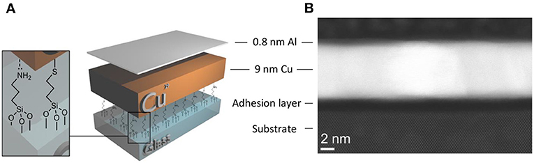
Figure 1. (A) Simplified schematic illustration of the electrode structure. (B) High resolution cross-sectional STEM (HR-STEM) image of a 9 nm Cu film with 0.8 nm Al overlayer supported on mixed silane adhesive layer derivatised Si wafer with native oxide. Both the Si atoms and rows of Cu atoms are resolved in the image.
In Figure 1B the Cu film is supported on the oxidized surface of a silicon wafer chemically derivatized with the mixed silane adhesion layer rather than silicate glass, to facilitate HR-STEM imaging and avoid image distortion due to charging. The native oxide at the surface of silicon has a very similar native hydroxyl density (onto which the mixed alkylsilane adhesion layer can bind) and chemical composition to that of silicate glass and so serves as a useful conducting substrate for STEM imaging (Aswal et al., 2006; Dietrich et al., 2015). Conventional wisdom is that Cu films deposited by thermal evaporation should be deposited at high vacuum to prevent contamination by residual gases and produce the most uniform films (Gao et al., 2014; McPeak et al., 2015). Consistent with this we have found that Cu films deposited at a base pressure of < 5 × 10⁻⁸ mbar are more conductive and stable (Figure S1) than those produced at higher pressure (5 × 10⁻⁶ mbar), and so all films in this study were deposited using < 5 × 10⁻⁸ mbar base pressure. On glass the surface roughness of a 9 nm thick Cu film measured over an area of 1 μm2 is reduced by one third when the substrate is derivatised with a monolayer of molecular adhesive from 1.44 ± 0.12 to 1.02 ± 0.05 nm, and the starting sheet resistance is reduced from 13.8 ± 0.6 to 10.8 ± 0.2 Ω sq−1, consistent with the formation of a more compact, uniform Cu film when using the molecular adhesive layer (Stec et al., 2011; Stec and Hatton, 2012; Hutter et al., 2013). For metal films of such low thickness the sheet resistance is strongly dependent on the thickness and quality of the metal film, and so small reductions in the metal thickness that result from surface oxidation can be monitored in real time via the film sheet resistance, making very thin slab-like metal films (like that in Figure 1) an ideal model to evaluate methods of passivating Cu as well as being of direct relevance as a window electrode for optoelectronics (Yun, 2017).
To date optically thin Ag supported on PEI (polyethylenimine) modified polyethylene terephthalate (PET) substrates are the best performing metal transparent electrode in terms of the transparency and sheet resistance (Kang et al., 2015; Jeong et al., 2017), and so this Ag electrode was used as a benchmark against which the stability of Cu electrodes can be evaluated. PEI has been shown to bind incident Ag atoms to a substrate by coordination bonds, and so serves the same function for Ag as the alkylsilane molecular adhesive layer used in the current study for Cu (Jeong et al., 2017). In this study we have translated this procedure to glass substrates for ease of substrate handing, achieving comparable sheet resistance and transparency to that reported on PET: 9.4 ± 0.3 Ω sq−1 (Table S1). Notably, Ag films supported on a PEI layer have a lower sheet resistance and higher transparency than those supported on an alkylsilane molecular adhesive layer: Figures S2, S3.
Figure 2 shows the evolution of the sheet resistance of 9 nm thick Cu and Ag films with time exposed to ambient air. The sheet resistance of the Cu film without an 0.8 nm Al overlayer increases rapidly from a starting resistance of 10.8 ± 0.2 Ω sq−1, and then more steadily at 0.0048 Ω sq−1 hr−1 due to surface oxidation (Iijima et al., 2006). Also shown is the stability of a 9 nm Ag film supported on a PEI nucleation layer fabricated using the method reported by Kang et al. (2015). The sheet resistance of the 9 nm Ag film increases continually at a rate of 0.0012 Ω sq−1 hr−1, which is significantly slower than the comparable Cu electrode. X-ray photoelectron spectroscopy analysis of Ag films aged for 2,000 h in air show that the oxidation products are primarily the sulfide Ag2SO4 and carbonate Ag2CO3, based on an assignment of the peaks at 168.5 and 288.8 eV, respectively, Table S2 and Figure S4. This is consistent with the findings of Sanders et al. (2015) for thick Ag films exposed to air for 720–1,440 h and corroborated by the corresponding oxygen components and concentrations at 531.5 and 530.7 eV, respectively. Notably, neither AgO or Ag2O are present in the O 1s spectrum (528.6, 529.5 eV), consistent with the hypothesis that silver oxide is only an intermediary for the formation of Ag2SO4 and AgCl (Sanders et al., 2015). It is also possible that morphological instability of the ultra-thin Ag films contributes to the deterioration in sheet resistance (Zhang et al., 2017).
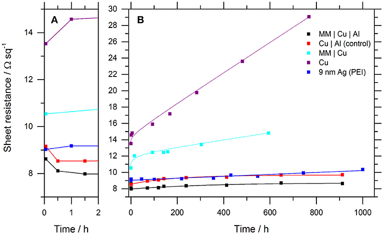
Figure 2. Evolution of the sheet resistance for representative Cu and Ag film electrodes stored in ambient air: (A) First 2 h expanded. (B) Extended 1,000-h test period. All Cu layers are 9 nm thick. Where Al forms part of the electrode it has a nominal thickness of 0.8 nm. The fitted lines are to guide-the-eye only. Table S1 and Figure S2 give the details of the complete data sets for all electrode structures. The temperature and humidity fluctuated in the range 18–30°C and 15–50%, respectively.
The initial sheet resistance of the 9 nm Cu film with an 0.8 nm Al overlayer is comparable to that of the 9 nm Ag film (8.7 ± 0.2, 9.4 ± 0.3 Ω sq−1), and more stable than that of Ag with a long-term rate of increase in sheet resistance of only 0.0009 Ω sq−1 hr−1 compared to 0.0012 Ω sq−1 hr−1 for Ag. The fact that the stability of the Cu electrode with an 0.8 nm Al overlayer is at least as good as that of the Ag electrode over this time period, a finding that is also translatable to flexible PET substrates (Table S1 and Figure S5), is of significant practical importance for emerging applications requiring the use of low cost transparent electrode materials. Notably, the sheet resistance of the Cu|Al electrode is below its starting value until ~600 h air exposure due to an initial sharp decrease in sheet resistance within the first 30 min Figure 2A. This unusual effect has previously been attributed to partial de-alloying of Al from the underlying Cu driven by Al oxidation: Hutter et al. (2013) have shown that even if the Al thickness on Cu is increased to 4.2 nm, Cu is still present at the surface of the bilayer film, showing that the Cu and Al mix when Al is evaporated directly onto Cu without breaking vacuum. The high solubility of Al in Cu is well-known to depend on temperature, and phase separation can occur when oversaturated, upon cooling or aging (Ralls et al., 1976; Marcus and Bower, 1997; Vaithyanathan et al., 2004). Since doping Cu with just 1% Al doubles the resistivity of Cu (Lanford et al., 1995), reducing the Al content of the alloyed interfacial layer would be expected to reduce the Cu film sheet resistance. Given that the Cu film is slab-like (as shown in Figure 1) the change in sheet resistance over 910 h, between the minimum at 1.5 h and after 912 h, is equivalent to a decrease in metal thickness of ~0.7 nm. This equates to an oxide thickness of ≤ 1 nm which is thin enough for electrons to efficiently tunnel across the oxide layer, ensuring the underlying metal does not become electrically isolated (Shewchun et al., 1977; Dabera et al., 2017).
It is reasonable to assume that the vacuum deposited Al is initially distributed uniformly over the Cu surface due to the high cohesive energy between metal atoms, where it at least partially alloys with the Cu, since Cu is well-known to readily alloy with Al (Ho et al., 1983; Li et al., 1991). Direct evidence that the Al initially forms a uniform layer is provided by surface roughness analysis of Cu films with and without a 0.8 nm Al layer: Table 1. In this experiment a molecular adhesive layer was deliberately not used, to ensure the Cu film has a significant surface roughness prior to Al evaporation. Samples were fabricated by deposition of Cu across all the glass substrates, followed by masking one half, without breaking vacuum, and evaporation of 0.8 nm Al.
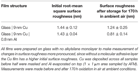
Table 1. A comparison of the roughness of electrodes with and without a 0.8 nm Al overlayer.
The surface roughness of Cu films with and without an Al overlayer is initially equal at 1.43 ± 0.04 and 1.44 ± 0.12 nm, respectively, consistent with conformal coverage of the Cu surface by Al which occurs due to the metallic bonding interaction between Cu and Al. It is known that Cu and Al readily diffuse into one another even at ambient temperature (Hutter et al., 2013) and so for such low Al thickness it is most likely that the Al is not a discrete layer, but rather an alloyed Al/Cu layer. After 170 h exposed to ambient air, the electrodes without the Al passivation layer show a ~14% reduction in average surface roughness from 1.44 ± 0.12 to 1.24 ± 0.25 nm, although notably the magnitude of this reduction falls within the spread of error. This decrease in surface roughness can be attributed to volume expansion associated with a gradual conversion of Cu to Cu oxides, since the density of Cu oxides is approximately one third lower than the metal (relative densities to [Cu]; [Cu2O] 0.67 and [CuO] 0.71) and so the gaps between Cu grains that give rise to the nanoscale surface roughness will be reduced to accommodate this extra volume. Conversely the electrodes with the 0.8 nm Al overlayer show a very pronounced ~43% decrease in surface roughness over the same period, which can only have resulted from a significant redistribution of metal atoms over the film surface, filling the gaps between Cu grains. Given that this large reduction in surface roughness only occurs for the Cu film with an Al over layer, the simplest explanation is that the Al component has gradually segregated to the grain boundaries in the Cu film surface. Direct evidence that, after an extended period in air, the Al is not uniformly distributed over the Cu surface but is concentrated at grain boundaries is provided by cross-sectional STEM images with corresponding nano-scale elemental analysis by energy-dispersive X-ray spectroscopy (EDXS) for a MM | Cu | Al film exposed to ambient air for 200 h: Table 1 and Figure 3.
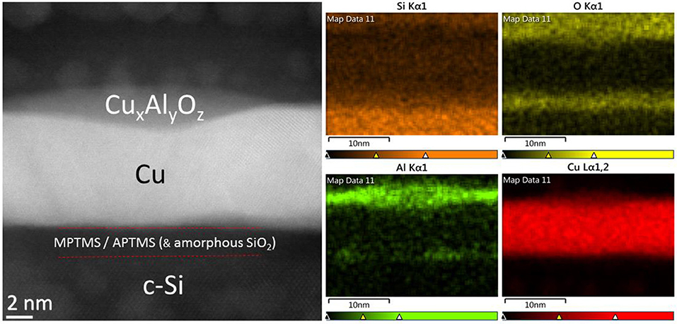
Figure 3. (Left) A HR-STEM image of a MM | Cu | Al film, supported on crystalline silicon, exposed to air for >170 h. (Right) (4)—Spatially resolved EDXS mapping of the STEM image for the elements Si, O, Al, and Cu.
It is evident from both the contrast image (Left) and elemental EDXA analysis (Right) in Figure 3, that after this extended period of air exposure the Al is not evenly distributed over the Cu surface (also evident in Figures S6, S7), but has segregated to Cu grain boundaries where it forms an oxide plug with a maximum thickness comparable to that of the self-limiting thickness of oxide on Al (2–3 nm) (Evertsson et al., 2015). Given that grain boundaries will be most susceptible to oxidation, both due to the higher radius of curvature and increased permeability of oxygen along grain boundaries, this accumulation at the grain boundaries explains the remarkable effectiveness of such a thin Al overlayer at passivating the underlying Cu: A copper-doped aluminium-oxide plug would be expected to serve as an effective local barrier to oxygen and moisture. The findings of the cross-sectional TEM imaging are also consistent with the ~43% decrease in surface roughness measured using AFM that occurs after exposure of the electrode to air, since filling the grain boundaries will inevitably reduce the surface roughness.
Electrode Patterning
For many practical applications it is necessary to pattern metal films, which risks undermining the effectiveness of a surface passivation layer. To investigate this conventional photolithography has been used to fabricate a regular array of 2 μm diameter holes in a 9 nm Cu film with and without a 0.8 nm Al over layer: Figure S8. The aperture density is ~6 million apertures per cm2 which increases the sheet resistance of the bilayer electrode from 8.7 ± 0.2 to 11.2 ± 0.4 Ω sq−1.
Figure 4 shows the normalized evolution of the sheet resistance of the patterned films upon exposure to ambient air. As expected the electrode without the 0.8 nm Al passivation layer oxidizes more quickly upon incorporation of apertures, with the sheet resistance increasing at a rate of 0.0071 Ω sq−1 hr−1. In contrast the stability of the MM | Cu | Al electrode is not adversely affected. After 5,000 h exposure to air, the sheet resistance stabilizes at < 1% of its starting value after patterning, and only 3.4% higher than its lowest value. It is concluded that the metal film with a high density of apertures has not undermined the effectiveness of the ultra-thin Al passivation layer, because the area of exposed Cu that is created by the inclusion of apertures is small (~5% increase) due to the very low metal film thickness.
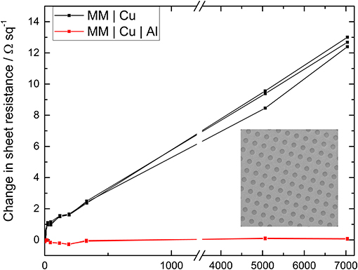
Figure 4. The change in sheet resistance of 9 nm Cu electrodes with an array of 2 μm diameter apertures (as shown in the inset) upon exposure to ambient air for Cu films with (red) and without (black) an 0.8 nm Al over layer. Full SEM images are given in Figure S8, together with the far-field transparency with and without apertures (Figure S9).
Conclusion
It has been shown that over 900 h in ambient air, unpatterned 9 nm thick Cu films passivated with an 0.8 nm evaporated Al layer are more stable than pure-Ag films of the same thickness fabricated using the best reported practice. Furthermore, after perforating with an array of ~6 million apertures per cm2, the sheet resistance after 5,000 h in air stabilizes at only 3.4% higher than its lowest value. The remarkable effectiveness of this approach is shown to result from segregation of aluminium-copper-oxide at the boundaries between Cu crystallites upon exposure to air, which retards oxidation at those sites in the Cu film most vulnerable to oxidation. Crucially, the very low thickness of this passivation layer ensures that the underlying metal is not electrically isolated, and so this simple passivation step renders Cu films stable enough to compete with Ag as the base metal for optically thin electrodes in emerging optoelectronic devices. By combining this approach to stabilizing optically thin Cu films with the previously reported methods for increasing far-field transparency (Hutter and Hatton, 2015; Kang et al., 2015; Pereira et al., 2018) the stage is set for using optically thin Cu films as a low cost transparent electrode in numerous emerging optoelectronic devices.
Author Contributions
PB conducted all of the experimental work (except for that stated below), analysed the data and wrote the manuscript. JL assisted with metal film deposition and developed the protocol for MPTMS derivatization of glass. SV assisted with lithographic patterning of the electrodes. HA performed the STEM and EDXS imaging and assisted with analysis. PB and MW performed the X-ray photoelectron spectroscopy and analysed the data. RH conceived the study and assisted with data analysis and writing the manuscript.
All data supporting this study are provided as supplementary information accompanying this paper.
Conflict of Interest Statement
The authors declare that the research was conducted in the absence of any commercial or financial relationships that could be construed as a potential conflict of interest.
Acknowledgments
The authors would like to thank the United Kingdom Engineering and Physical Sciences Research Council (EPSRC) for funding (Grant number: EP/N009096/1 & EP/N509796/1).
Supplementary Material
The Supplementary Material for this article can be found online at: https://www.frontiersin.org/articles/10.3389/fmats.2018.00071/full#supplementary-material
All data supporting this study are provided as supplementary information accompanying this paper.
Footnotes
1. ^ Nasdaq. Nasdaq: Commodity Prices. Available online at: http://www.nasdaq.com/markets/commodities.aspx (Accessed February 17, 2017).
References
Aswal, D. K., Lenfant, S., Guerin, D., Yakhmi, J. V., and Vuillaume, D. (2006). Self assembled monolayers on silicon for molecular electronics. Anal. Chim. Acta 568, 84–108. doi: 10.1016/j.aca.2005.10.027
Behrendt, A., Friedenberger, C., Gahlmann, T., Trost, S., Becker, T., Zilberberg, K., et al. (2015). Highly robust transparent and conductive gas diffusion barriers based on tin oxide. Adv. Mater. 27, 5961–5967. doi: 10.1002/adma.201502973
Biesinger, M. C., Lau, L. W. M., Gerson, A. R., and Smart, R. S. C. (2010). Resolving surface chemical states in XPS analysis of first row transition metals, oxides and hydroxides: Sc, Ti, V, Cu and Zn. Appl. Surf. Sci. 257, 887–898. doi: 10.1016/j.apsusc.2010.07.086
Chawla, S. K., Rickett, B. I., Sankarraman, N., and Payer, J. H. (1992). An X-ray photo-electron spectroscopic investigation of the air-formed film on copper. Corros. Sci. 33, 1617–1631. doi: 10.1016/0010-938X(92)90038-5
Chen, Z., Ye, S., Stewart, I. E., and Wiley, B. J. (2014). Copper nanowire networks with transparent oxide shells that prevent oxidation without reducing transmittance. ACS Nano 8, 9673–9679. doi: 10.1021/nn504308n
Dabera, G. D. M. R., Walker, M., Sanchez, A. M., Pereira, H. J., Beanland, R., and Hatton, R. A. (2017). Retarding oxidation of copper nanoparticles without electrical isolation and the size dependence of work function. Nat. Commun. 8:1894. doi: 10.1038/s41467-017-01735-6
Dennler, G., Lungenschmied, C., Neugebauer, H., Sariciftci, N. S., Latrèche, M., Czeremuszkin, G., et al. (2006). A new encapsulation solution for flexible organic solar cells. Thin Solid Films 511–512, 349–353. doi: 10.1016/j.tsf.2005.12.091
Dietrich, P. M., Streeck, C., Glamsch, S., Ehlert, C., Lippitz, A., Nutsch, A., et al. (2015). Quantification of silane molecules on oxidized silicon: are there options for a traceable and absolute determination? Anal. Chem. 87, 10117–10124. doi: 10.1021/acs.analchem.5b02846
Ellmer, K. (2012). Past achievements and future challenges in the development of optically transparent electrodes. Nat. Photon. 6, 809–817. doi: 10.1038/NPHOTON.2012.282
Evertsson, J., Bertram, F., Zhang, F., Rullik, L., Merte, L. R., Shipilin, M., et al. (2015). The thickness of native oxides on aluminum alloys and single crystals. Appl. Surf. Sci. 349, 826–832. doi: 10.1016/j.apsusc.2015.05.043
Gan, L., Gomez, R. D., Castillo, A., Chen, P. J., Powell, C. J., and Egelhoff, W. F. (2002). Ultra-thin aluminum oxide as a thermal oxidation barrier on metal films. Thin Solid Films 415, 219–223. doi: 10.1016/S0040-6090(02)00622-3
Gao, T., Wang, B., Ding, B., Lee, J. K., and Leu, P. W. (2014). Uniform and ordered copper nanomeshes by microsphere lithography for transparent electrodes. Nano Lett. 14, 2105–2110. doi: 10.1021/nl5003075
Gao, W., Gong, H., He, J., Thomas, A., Chan, L., and Li, S. (2001). Oxidation behaviour of Cu thin films on Si wafer at 175 – 400°C. Mater. Lett. 51, 78–84. doi: 10.1016/S0167-577X(01)00268-3
Gattinoni, C., and Michaelides, A. (2015). Atomistic details of oxide surfaces and surface oxidation: the example of copper and its oxides. Surf. Sci. Rep. 70, 424–447. doi: 10.1016/j.surfrep.2015.07.001
Ghosh, D. S. (2013). Ultrathin Metal Transparent Electrodes for the Optoelectronics Industry. Heidelberg: Springer International Publishing. doi: 10.1007/978-3-319-00348-1
Griffith, M. J., Cooling, N. A., Vaughan, B., Elkington, D. C., Hart, A. S., Lyons, A. G., et al. (2016). Combining printing, coating, and vacuum deposition on the roll-to-roll scale: a hybrid organic photovoltaics fabrication. IEEE J. Sel. Top. Quant. Electron. 22:4100714. doi: 10.1109/JSTQE.2015.2487968
Ho, C. Y., Ackerman, M. W., Wu, K. Y., Havill, T. N., Bogaard, R. H., Matula, R. A., et al. (1983). Electrical resistivity of ten selected binary alloy systems. J. Phys. Chem. Ref. Data 12, 183–322. doi: 10.1063/1.555684
Hsu, P. C., Wu, H., Carney, T. J., McDowell, M. T., Yang, Y., Garnett, E. C., et al. (2012). Passivation coating on electrospun copper nanofibers for stable transparent electrodes. ACS Nano 6, 5150–5156. doi: 10.1021/nn300844g
Hutter, O. S., and Hatton, R. A. (2015). A hybrid copper:tungsten suboxide window electrode for organic photovoltaics. Adv. Mater. 27, 326–331. doi: 10.1002/adma.201404263
Hutter, O. S., Stec, H. M., and Hatton, R. A. (2013). An indium-free low work function window electrode for organic photovoltaics which improves with in-situ oxidation. Adv. Mater. 25, 284–288. doi: 10.1002/adma.201203280
Iijima, J., Lim, J. W., Hong, S. H., Suzuki, S., Mimura, K., and Isshiki, M. (2006). Native oxidation of ultra high purity Cu bulk and thin films. Appl. Surf. Sci. 253, 2825–2829. doi: 10.1016/j.apsusc.2006.05.063
Jeong, S., Jung, S., Kang, H., Lee, D., Choi, S., Kim, S., et al. (2017). Role of polymeric metal nucleation inducers in fabricating large-area, flexible, and transparent electrodes for printable electronics. Adv. Funct. Mater. 27, 1–8. doi: 10.1002/adfm.201606842
Kang, H., Jung, S., Jeong, S., Kim, G., and Lee, K. (2015). Polymer-metal hybrid transparent electrodes for flexible electronics. Nat. Commun. 6, 6503–6510. doi: 10.1038/ncomms7503
Khan, A., Nguyen, V. H., Muñoz-Rojas, D., Aghazadehchors, S., Jiménez, C., Nguyen, N. D., et al. (2018). Stability enhancement of silver nanowire networks with conformal ZnO coatings deposited by atmospheric pressure spatial atomic layer deposition. ACS Appl. Mater. Interf. 10, 19208–19217. doi: 10.1021/acsami.8b03079
Kim, H., Horwitz, J. S., Kushto, G. P., Kafafi, Z. H., and Chrisey, D. B. (2001). Indium tin oxide thin films grown on flexible plastic substrates by pulsed-laser deposition for organic light-emitting diodes. Appl. Phys. Lett. 79, 284–286. doi: 10.1063/1.1383568
Kim, J. B., Kim, C. S., Kim, Y. S., and Loo, Y-L. (2009). Oxidation of silver electrodes induces transition from conventional to inverted photovoltaic characteristics in polymer solar cells. Appl. Phys. Lett. 95, 183301–183303. doi: 10.1063/1.2212270
Krebs, F. C., Espinosa, N., Hösel, M., Søndergaard, R. R., and Jørgensen, M. (2014). 25th anniversary article: rise to power - OPV-based solar parks. Adv. Mater. 26, 29–39. doi: 10.1002/adma.201302031
Lanford, W. A., Ding, P. J., Wang, W., Hymes, S., and Muraka, S. P. (1995). Low-temperature passivation of copper by doping with Al or Mg. Thin Solid Films 262, 234–241. doi: 10.1016/0040-6090(95)05837-0
Lee, C., Kim, N. R., Koo, J., Lee, Y. J., and Lee, H. M. (2015). Cu-Ag core-shell nanoparticles with enhanced oxidation stability for printed electronics. Nanotechnology 26:455601. doi: 10.1088/0957-4484/26/45/455601
Li, J., Mayer, J. W., and Colgan, E. G. (1991). Oxidation and protection in copper and copper alloy thin films. J. Appl. Phys. 70, 2820–2827. doi: 10.1063/1.349344
Lu, H., Ren, X., Ouyang, D., and Choy, W. C. H. (2018). Emerging novel metal electrodes for photovoltaic applications. Small 14:1703140. doi: 10.1002/smll.201703140
Lu, M., Huang, S., Chen, S., Ju, Q., Xiao, M., Peng, X., et al. (2018). Transparent and super-gas-barrier PET film with surface coated by a polyelectrolyte and Borax. Polym. J. 50, 239–250. doi: 10.1038/s41428-017-0015-5
Marcus, M. A., and Bower, J. E. (1997). Precipitation of Al2Cu in blanket Al-Cu films. J. Appl. Phys. 82, 3821–3827. doi: 10.1063/1.365745
Matula, R. A. (1979). Electrical resistivity of cooper, gold, palladium and silver. J. Phys. Chem. 8, 1147–1298. doi: 10.1063/1.555614
McPeak, K. M., Jayanti, S. V., Kress, S. J. P., Meyer, S., Iotti, S., Rossinelli, A., et al. (2015). Plasmonic films can easily be better: rules and recipes. ACS Photon. 2, 326–333. doi: 10.1021/ph5004237
Mugwang'a, F. K., Karimi, P. K., Njoroge, W. K., Omayio, O., and Waita, S. M. (2013). Optical characterization of Copper Oxide thin films prepared by reactive dc magnetron sputtering for solar cell applications. Int. J. Thin Film. Sci. Technol. 2, 12–24. doi: 10.1016/S0042-207X(00)00151-2
Mulligan, C. J., Wilson, M., Bryant, G., Vaughan, B., Zhou, X., Belcher, W. J., et al. (2013). A projection of commercial-scale organic photovoltaic module costs. Sol. Energy Mater. Sol. Cells 120, 9–17. doi: 10.1016/j.solmat.2013.07.041
O'Reilly, M., Jiang, X., Beechinor, J. T., Lynch, S., NíDheasuna, C., Patterson, J. C., et al. (1995). Investigation of the oxidation behaviour of thin film and bulk copper. Appl. Surf. Sci. 91, 152–156. doi: 10.1016/0169-4332(95)00111-5
Pereira, H. J., Reed, J., Lee, J., Varagnolo, S., Dabera, G. D. M. R., and Hatton, R. A. (2018). Fabrication of Copper window electrodes with 108 Apertures per cm2 for organic photovoltaics. Adv. Funct. Mater 28:1802893. doi: 10.1002/adfm.201802893
Platzman, I., Brener, R., Haick, H., and Tannenbaum, R. (2008). Oxidation of polycrystalline copper thin films at ambient conditions. J. Phys. Chem. C 112, 1101–1108. doi: 10.1021/jp076981k
Ralls, K., Courtney, T., and Wulff, J. (1976). Introduction to Materials Science and Engineering. New York, NY: John Wiley & Sons.
Sahu, D. R., and Huang, J. L. (2006). Dependence of film thickness on the electrical and optical properties of ZnO-Cu-ZnO multilayers. Appl. Surf. Sci. 253, 915–918. doi: 10.1016/j.apsusc.2006.01.035
Sanders, C. E., Verreault, D., Frankel, G. S., and Allen, H. C. (2015). The Role of Sulfur in the atmospheric corrosion of silver. J. Electrochem. Soc. 162, C630–C637. doi: 10.1149/2.0051512jes
Sannicolo, T., Lagrange, M., Cabos, A., Celle, C., Simonato, J. P., and Bellet, D. (2016). Metallic nanowire-based transparent electrodes for next generation flexible devices: a review. Small 12, 6052–6075. doi: 10.1002/smll.201602581
Shewchun, J., Singh, R., and Green, M. A. (1977). Theory of metal-insulator-semiconductor solar cells. J. Appl. Phys. 48, 765–770. doi: 10.1063/1.323667
Sivaramakrishnan, K., and Alford, T. L. (2009). Metallic conductivity and the role of copper in ZnO/Cu/ZnO thin films for flexible electronics. Appl. Phys. Lett. 94, 2104–2106. doi: 10.1063/1.3077184
Stec, H. M., and Hatton, R. A. (2012). Widely applicable coinage metal window electrodes on flexible polyester substrates applied to organic photovoltaics. ACS Appl. Mater. Inter. 4, 6013–6020. doi: 10.1021/am3016763
Stec, H. M., Williams, R. J., Jones, T. S., and Hatton, R. A. (2011). Ultrathin transparent Au electrodes for organic photovoltaics fabricated using a mixed mono-molecular nucleation layer. Adv. Funct. Mater. 21, 1709–1716. doi: 10.1002/adfm.201002021
Stewart, I. E., Ye, S., Chen, Z., Flowers, P. F., and Wiley, B. J. (2015). Synthesis of Cu-Ag, Cu-Au, and Cu-Pt Core-shell nanowires and their use in transparent conducting films. Chem. Mater. 27, 7788–7794. doi: 10.1021/acs.chemmater.5b03709
Tyler, M. S., Hutter, O. S., Walker, M., and Hatton, R. A. (2015). A silver-free, reflective substrate electrode for electron extraction in top-illuminated organic photovoltaics. ChemPhysChem 16, 1203–1209. doi: 10.1002/cphc.201402880
Vaithyanathan, V., Wolverton, C., and Chen, L. Q. (2004). Multiscale modeling of θ′ precipitation in Al-Cu binary alloys. Acta Mater. 52, 2973–2987. doi: 10.1016/j.actamat.2004.03.001
Watanabe, M., Watanabe, H., Ando, H., Handa, T., Ichino, T., and Kuwakiet, N. (2007). Comparative XPS Study of silver and copper surfaces exposed to flowing air containing low concentration of sulfur dioxide. Zairyo-to-Kankyo 56, 10–15. doi: 10.3323/jcorr.56.10
Wiame, F., Maurice, V., and Marcus, P. (2007). Initial stages of oxidation of Cu(111). Surf. Sci. 601, 1193–1204. doi: 10.1016/j.susc.2006.12.028
Young, F. W., Cathcart, J. V., and Gwathmey, A. T. (1956). The rates of oxidation of several faces of a single crystal of copper as determined with elliptically polarized light. Acta Metall. 4, 145–152. doi: 10.1016/0001-6160(56)90132-8
Yun, J. (2017). Ultrathin metal films for transparent electrodes of flexible optoelectronic devices. Adv. Funct. Mater. 27:1606641. doi: 10.1002/adfm.201606641
Zhang, C., Kinsey, N., Chen, L., Ji, C., Xu, M., Ferrera, M., et al. (2017). High-performance doped silver films: overcoming fundamental material limits for nanophotonic applications. Adv. Mater. 29:1605177. doi: 10.1002/adma.201605177
Zhang, C., Zhao, D., Gu, D., Kim, H., Ling, T., Wu, Y. K. R., et al. (2014). An ultrathin, smooth, and low-loss Al-doped Ag film and its application as a transparent electrode in organic photovoltaics. Adv. Mater. 26, 5696–5701. doi: 10.1002/adma.201306091
Zhao, G., Kim, S. M., Lee, S. G., Bae, T. S., Mun, C. W., Lee, S., et al. (2016). Bendable solar cells from stable, flexible, and transparent conducting electrodes fabricated using a nitrogen-doped ultrathin copper film. Adv. Funct. Mater. 26, 4180–4191. doi: 10.1002/adfm.201600392
Keywords: copper, passivation, thin film, lithography, transparent electrode
Citation: Bellchambers P, Lee J, Varagnolo S, Amari H, Walker M and Hatton RA (2018) Elucidating the Exceptional Passivation Effect of 0.8 nm Evaporated Aluminium on Transparent Copper Films. Front. Mater. 5:71. doi: 10.3389/fmats.2018.00071
Received: 14 August 2018; Accepted: 05 November 2018;
Published: 04 December 2018.
Edited by:
Hyung-Ho Park, Yonsei University, South KoreaReviewed by:
Ho Won Jang, Seoul National University, South KoreaWon Il Park, Hanyang University, South Korea
Hong-Sub Lee, Kangwon National University, South Korea
Copyright © 2018 Bellchambers, Lee, Varagnolo, Amari, Walker and Hatton. This is an open-access article distributed under the terms of the Creative Commons Attribution License (CC BY). The use, distribution or reproduction in other forums is permitted, provided the original author(s) and the copyright owner(s) are credited and that the original publication in this journal is cited, in accordance with accepted academic practice. No use, distribution or reproduction is permitted which does not comply with these terms.
*Correspondence: Ross A. Hatton, ross.hatton@warwick.ac.uk
†Present Address: Houari Amari, Imaging Center at Liverpool (ICaL), School of Engineering & School of Physical Sciences, University of Liverpool, Liverpool, United Kingdom