Review of Printed Electrodes for Flexible Devices
 Quanling Li1† Jiayan Zhang1† Qianhao Li1 Guihong Li2 Xiyue Tian1 Zewei Luo1 Fei Qiao2
  Xing Wu1* Jian Zhang1*
- 1Shanghai Key Laboratory of Multidimensional Information Processing, Department of Electronic Engineering, East China Normal University, Shanghai, China
- 2Department of Electronic Engineering, Tsinghua University, Beijing, China
Printed electronic technologies draw tremendous attention worldwide due to their ability to surpass the limitations of traditional high-cost electronics, based on rigid silicon, and the manufacturing of various devices on flexible substrates. As a critical component of flexible electronics, electrodes fabricated on soft, bendable, and stretchable substrates are of great importance. Based on the fabrication process, this paper classifies the mainstream technologies into two categories: top-down and bottom-up. Top-down technologies include physical evaporation methods, printing technologies and soft lithography, while bottom-up technologies involve polymer-assisted-metal-deposition methods and ion-exchange methods, respectively. In contrast to top-down technologies that transfer functional ink onto substrates directly, the bottom-up method achieves a great improvement in the adhesion between substrates and metal electrodes. In this paper, the challenges of top-down technologies, including cost, synthesis, and choice of ink for printing technologies, the limited choice of metal for bottom-up technologies and the mass production of these methods, are also discussed.
Introduction
Increasing demand for high performance devices, drives the development of alternative, or novel structures of devices and the use of new materials (Liu et al., 2017; Wang et al., 2018). In recent years, flexible and stretchable electronics have developed at an unprecedented rate and are involved in various applications, including sensors (Chu et al., 2018; Pan et al., 2018), displays (Chen et al., 2017), solar cells (Wang C. et al., 2017; Xi et al., 2017; Zhang et al., 2017), supercapacitors (Li J. et al., 2017; Wang M. et al., 2017), electronic skins (E-skins) (Lou et al., 2017; Bermúdez et al., 2018; Byun et al., 2018) and wearable electronics (Lee et al., 2017). Some applications are shown in Figure 1. In terms of substrates, conventional silicon, and mature technologies have attained micro structures and ultrathin chips, which strengthen its flexibility (Lin C. C. et al., 2017; Navaraj et al., 2018). However, compared with this complicated process, the method for fabricating devices directly on the soft, bendable and skin-mounted polymer substrates, such as polyethylene (PE) and terephthalate (PET) is more advantageous. In the realization process of the devices mentioned above, a key challenge in producing electrodes, with high conductivity and good flexibility, exists. To solve this problem, some solutions are being developed. These solutions include conventional technologies derived from mature technologies for silicon substrates, such as physical vapor deposition, printing technologies such as screen and inkjet printing technologies, and roll-to-roll technology, spin-coating method, and other technologies that contain chemical procedures.
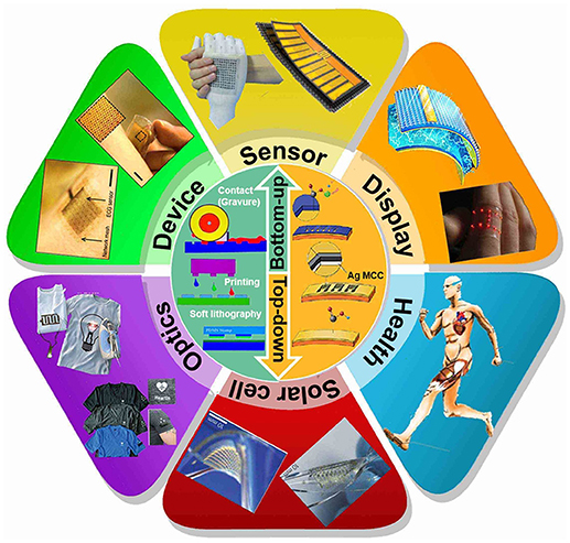
Figure 1. Two strategies for fabricating flexible electrodes and the products that use electrodes. These technologies include both top-down and bottom-up methods. The top-down method involves electrode materials being deposited on the substrate by various physical methods. The bottom-up method involves an ion-exchange between the electrode materials and the electrode ions which grow from the bottom. The technology of flexible electrode fabrications can be applied to different devices (Jang et al., 2015). Reproduced with the permission of 2015 Macmillan Publishers Limited. These devices include flexible sensors (Jang et al., 2014; Zhang et al., 2015), flexible display screens (Gao et al., 2016; Leung et al., 2018), human health detection devices (Wang X. et al., 2017), solar cells (Son et al., 2014), and optical clothes (Lee et al., 2018). Reproduced with the permission of 2015 Macmillan Publishers Limited, 2014 Macmillan Publishers Limited, 2016 Macmillan Publishers Limited, 2018 WILEY-VCH Verlag GmbH & Co. KGaA, Weinheim, 2017 Wiley-VCH Verlag GmbH & Co. KGaA, Weinheim, 2014 Macmillan Publishers Limited, 2018 WILEY-VCH Verlag GmbH & Co. KGaA, Weinheim, respectively.
Depending on the fabrication of electrodes, the subsistent technologies are classified into two categories: the top-down and bottom-up. The aim of this paper is to review the current processes of fabricating flexible electrodes within these two categories. As shown in Figure 2, top-down methods include traditional technologies, printing technologies and soft lithography, while the bottom-up method includes the polymer-assisted-metal-deposition (PAMD) technology and ion-exchange technology. To be specific, top-down methods use physical methods to pile electrode material up on the substrate. In other words, electrode material originates from the source above the substrates and is deposited on the substrate, most of which is a physical process. In contrast, bottom-up methods use chemical methods to fabricate flexible electrodes. Take the ion-exchange method as an example, the substrate is processed by a chemical method to an ion exchange between the electrode material and the substrate. Some ions of the electrode materials replace the ions of the substrate. The ions of the electrode material grows upward and forms the electrodes. Furthermore, Figure 1 lists the various products that use the technology of flexible electrode fabrication. The flexible electrodes can be applied to flexible devices. Flexible devices include sensors, display screens and solar cells (Son et al., 2014). These devices can be used to compose wearable devices that can monitor human health. Flexible electrodes are capable of working in a variety of applications. Fabricating high-performance flexible electrodes is necessary during the development of electronic devices.
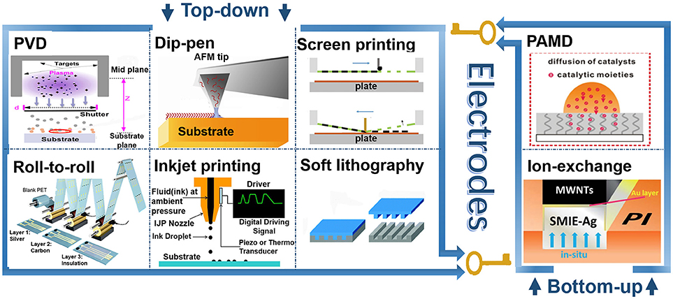
Figure 2. The technologies for electrode fabrication, including two categories based on the manufacture process: top-down and bottom-up. Top-down technologies involving the physical evaporation deposition (Sahu et al., 2018), dip-pen nanolithography, (Wixforth et al., 2009), screen printing technology (Li W. et al., 2017), roll-to-roll technology (Bariya et al., 2018), inkjet printing technology (Xu et al., 2007), and the soft lithography (Wisser et al., 2015). Reproduced with the permission of 2018 Springer Nature Limited, SPIE Europe Microtechnologies, The Royal Society of Chemistry 2017, 2018 American Chemical Society, SPIE Europe Microtechnologies, The Royal Society of Chemistry 2015.
The Top-Down Technologies of Printed Electrodes
Conventional Technologies
Physical Evaporation Deposition
The traditional production process for RFID antennas is demonstrated in Figure 3A (Wu, 2017). The fabrication process, based on rigid silicon substrates, involves complicated steps as well as the use of chemical reagents. Contrarily, due to the common character of flexible substrates that cannot bear high temperature and reagent corrosion, the preparation of electrodes on flexible substrates is usually simple. Nonetheless, depending on the mature production technology, traditional methods of fabricating electrodes are still informative and compatible with electrodes on flexible substrates. Physics vapor deposition (PVD), which includes three main techniques, evaporation, sputtering and electron beam irradiation (e-beam), is one of the most popular methods for depositing metal electrodes. As shown in Figures 3B,C, Yeongin Kim et al. reported a bioinspired flexible organic artificial afferent nerve, which includes a core composed of organic ring oscillators (Kim et al., 2018). In the process of producing the organic ring oscillators, Ti/Al were deposited as gate electrodes and patterned Cr/Au were deposited as source/drain electrodes, both of which were fabricated by e-beam. Sungjun Park et al. reported fabricating self-powered, ultra-flexible electronics via nanograting-patterned organic photovoltaics, with deposited 100 nm indium tin oxides (ITO) electrode (Park et al., 2018). These widely-used traditional technologies are compatible with the production of flexible electrodes. In addition, by relying on these mature physical techniques, the fabricated electrodes pose a high nanoscale solution and relatively high conductivity, which is suitable for refined applications. It is therefore noteworthy that the deposition of metal is usually a one-step deposition. In classic top-down methods for depositing metal on flexible substrates, the physical adhesion between the electrodes and the substrates is usually weaker than those fabricated with the bottom-up methods.
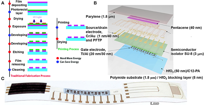
Figure 3. (A) Schematic fabrication illustration of RFID antennas using traditional techniques (Wu, 2017). Reproduced with the permission of Royal Society of Chemistry 2017. (B) Device structure of organic ring oscillators of the artificial system with deposited Cr/Au as source/drain electrodes. (C) A photograph of an artificial afferent system (Kim et al., 2018). Reproduced with the permission of 2018 American Association for the Advancement of Science.
Dip-Pen Technology
The mechanism of the dip-pen nanolithography can be described as ink molecules that attach to the tip of the atomic force microscope and are gradually transferred to the surface of the substrate, to achieve controllable patterns with the assistance of the capillary action and surface tension of the water droplets between the tip and the base. Lina et al reported fabricating the Au nanostructure array using the dip-pen method as a desktop fabrication tool, making it possible for high-throughput and arbitrary patterns in an ambient condition (Chen et al., 2017). Figure 4A is the fabrication diagram of Au structure employing the dip-pen technology. Figure 4B shows the atomic force microscope (AFM) topography of PMMA brushes under various patterning conditions, which is employed as a mask for chemical etching in the fabrication procedures shown in Figure 4A. Figure 4C shows the AFM topography of resulting Au structures. Cronin et al reported fabricating the ZnO dot array on the flexible PE substrates (Cronin et al., 2014). Figure 4D is the scanning electron microscope (SEM) image of the ZnO dot with a ~10 μm diameter. Figure 4E is the enlarged SEM image of sample shown in Figure 4D. The EDX area analysis validates the presence of Zn and O shown in Figure 4F. The AFM image of the dot is shown in Figure 4G, demonstrating the roughness of the dot fabricated with ZnO ink. In addition, it can be observed that the maximum size of the fabricated dot is ~350 nm. In Figure 4H, the bent PE substrate and conducting ZnO array is displayed, after a versatile transfer process, and illustrates the enlarged view of the patterned arrays, to the right.
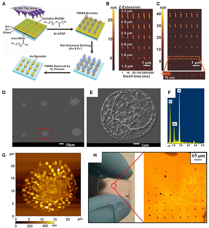
Figure 4. (A) The fabrication of Au nanostructures, by parallel dip-pen nanodisplacement lithography, surface-initiated atom transfer radical polymerization and wet-chemical etching. (B,C) AFM topography of PMMA brushes and the Au structures (Chen et al., 2017). Reproduced with the permission of WILEY-VCH Verlag GmbH & Co. KGaA, Weinheim. (D) SEM images of ZnO array. (E) Magnified image of SEM image. (F) Energy Dispersive X-Ray (EDX) Spectrum of ZnO dot in (E). (G) AFM image of the ZnO dot. (H) Digital image of the bent polyethylene naphthalate (PEN) substrate with deposited ZnO dot array (Cronin et al., 2014). Reproduced with the permission of 2018 Elsevier B.V.
Printing Technologies
Due to high costs and the demanding requirements of machines for the electrodes fabricated by conventional technologies, low-cost fabrication methods are desired. Here, low cost, high efficiency printing fabrication processes are reviewed.
Screen Printing Technology
In this relatively mature technology, shown in Figure 5A, there are five core components including a stencil with meshes, a squeegee, functional ink, a screen printer stage and substrate. As shown in Figures 5B,C, the procedure of screen-printing involves two main steps: the penetration of functional ink through the mesh in the stencil and the deposition onto the substrate, thereby forming the requisite patterned electrodes. The cross-section process of screen-printing technology is demonstrated in Figure 5D.
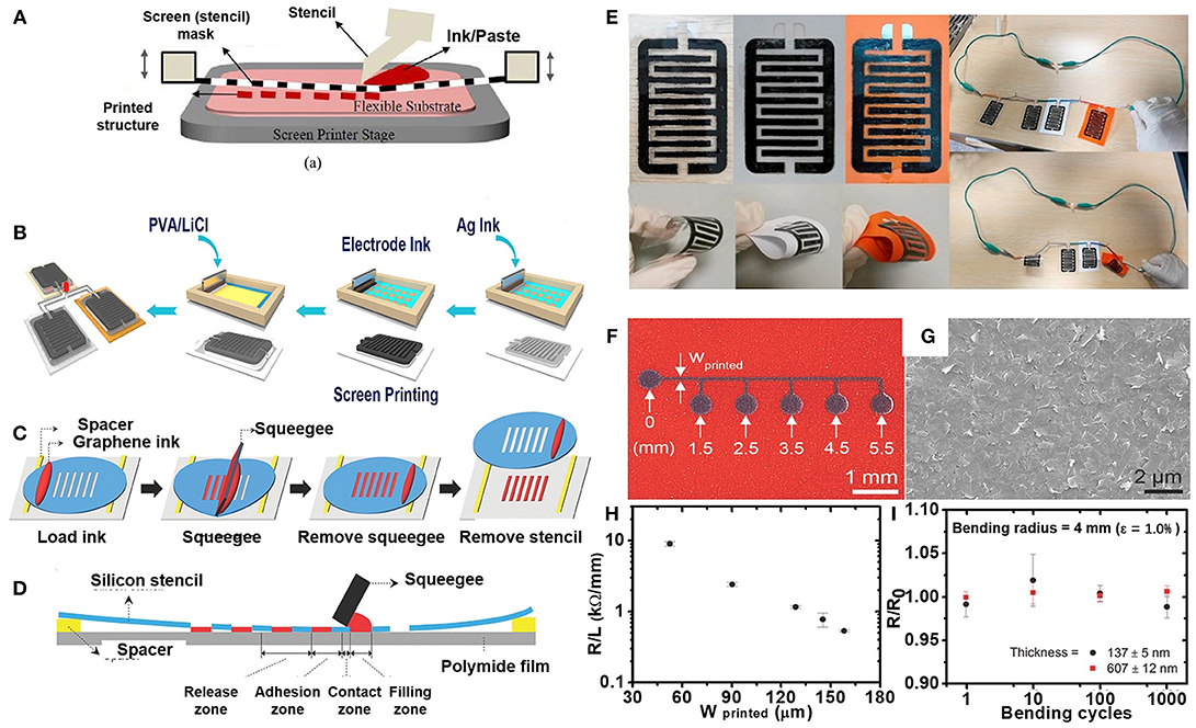
Figure 5. (A) The illustration of screen printing technology (Khan et al., 2015). Reproduced with the permission of the IEEE. (B) The diagram of fabrication of the transistor (Lu et al., 2017). Reproduced with the permission of 2017 Elsevier B.V. (C) Schematic fabrication process of electrodes using screen printing technology and graphene ink. (D) Cross-sectional diagram of the screen printing technique (Hyun et al., 2015a). Reproduced with the permission of 2015 WILEY-VCH Verlag GmbH & Co. KGaA, Weinheim. (E) Optical photographs of printed electrodes fabricated using the screen-printing technology shown in (B) (Lu et al., 2017). Reproduced with the permission of 2017 Elsevier B.V. (F) Optical micrograph of printed graphene lines with various printed widths. (G) SEM images of the graphene line surface. (H) Resistance per unit length of the graphene as a function of printed width. (I) Relative resistance changes of the graphene lines with different thicknesses under bending (Hyun et al., 2015a). Reproduced with the permission of 2015 WILEY-VCH Verlag GmbH & Co. KGaA, Weinheim.
Employing screen-printing technology, Qiang Lu et al. reported synthesizing composites of FeOOH/MnO2 as ink and fabricating all printed solid-state flexible supercapacitors (Lu et al., 2017). Due to the flexibility of PET, paper and textile as substrates, the supercapacitors are bendable as shown in Figure 5E. An experiment of illuminating a yellow LED, using printed electrodes, is also shown in Figure 5E. In addition to the composites of FeOOH/MnO2, graphene ink used in screen-printing technology has been reported by Hyun et al. (2015a). To improve the solution of graphene electrodes, a new way of making stencils was developed. A silicon wafer was thinned to 120 μm and then photolithography was carried out to pattern the surface with openings of various widths. The optical micrographs of printed graphene electrodes with varying widths and SEM images of the graphene electrode surface are shown in Figures 5F,G, respectively. The roughness of the electrodes was measured as ~ 32 nm using atomic force microscopy (AFM). Figure 5H focuses on the changes in resistance with different printed widths. The stability of electrodes under bending and releasing cycles is displayed in Figure 5I, shows the great bending stability of printed graphene, independent of the printed line widths. Limited to the penetration and block mechanism, patterned electrodes have the ability to transfer shapes accurately with the opening. Benefiting from a relatively simple procedure, feasibility of mass production, changeable patterns and low cost, screen printing technology is one of the most popular methods to fabricate electrodes on flexible substrates. Similar to the traditional method of fabricating electrodes, screen-printing technology also falls under the top-down methods. Due to the weak connection between the ink and the substrate, the viscosity and squeegee play a significant role in the solution.
Roll-To-Roll Technology
To satisfy the increasing need for industrial manufacturing, the roll-to-roll printing technology has been developed over the past years. Roll-to-roll printing technology features mass and pipeline production techniques that are put into use in a printed circuit board.
With functional ink printed onto flexible substrates, this physical fabrication process is also a type of top-down method. Bae et al reported using a roll-to-roll printing technology to fabricate transparent graphene electrodes as illustrated in Figure 6A (Bae et al., 2010). The whole process of fabrication involves three essential steps: adhesion of the polymer support to the graphene, removal of the Cu foil by etching, and release of the polymer support and transfer of the graphene onto the target substrates. A 30-inch graphene electrode film can be fabricated with a resistance of ~125 Ω−1 and 97.4% optical transmittance. In addition to the graphene, silver nanofiber ink is also employed to print electrodes. Figure 6B is a digital photograph of silver nanofiber electrodes using roll-to-roll technology, demonstrating its character of transparency and larger-size. SEM images of silver nanofibers are shown in Figure 6C. In Figure 6D, it can be observed that compared with other transparent electrodes, such as ITO, Ag nanotrough, graphene, carbon nanotubes and PEDOT:PSS, the fabricated electrodes have the advantage of transmittance and sheet resistance. In addition, by adjusting the spray time of the ink, the transmittance can be controlled. The demonstration of the experiment of LED illumination is shown in Figure 6E. Compared with the Ag film, the silver nanofiber has greater mechanical stability and conductivity under consecutive stretching and bending shown in Figure 6F. Benefiting from the intrinsic flexibility shown in the SEM images of Figure 6G, the nanofiber electrodes can bear over 2,000 s of bend and release cycles while maintaining the resistance, as shown in Figure 6H. Using the roll-to-roll fabrication technology, functional ink can be printed onto the substrate, forming flexible electrodes in a highly efficient way. The fabricated electrodes maintain a high transmittance and excellent flexibility while possessing a relatively high conductivity, which is very beneficial for display applications. Maintaining high productivity and high n at the same time is the predominant advantage of roll-to-roll technology, which can meet the demanding needs of mass production. The same can be said for other physical processes, where the electrodes show a relatively weak adhesion with the flexible substrates.
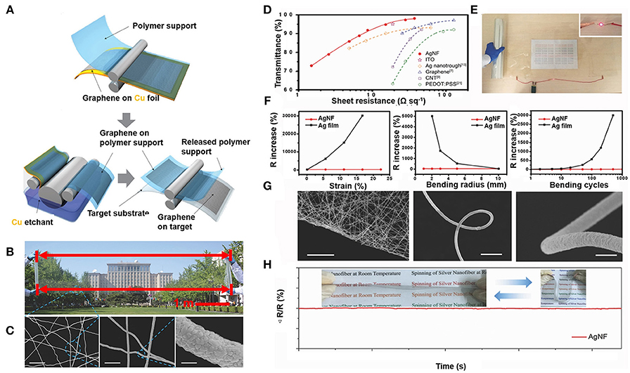
Figure 6. (A) Diagram of roll-to-roll printing for screen-printing (Bae et al., 2010). Reproduced with the permission of 2010 Macmillan Publishers Limited. (B) Optical images of silver nanofiber electrodes. (C) SEM images of silver nanofibers. (D) Comparison of sheet resistivity among silver fiber electrodes and other transparent electrodes. (E) Demonstration of LED illuminance utilizing fabricated electrodes. (F) Variations in the sheet resistance of silver nanofibers and Ag on PET substrates under varying bending radii. (G) SEM images of silver nanofibers under bending. (H) The stability test of a conductive tape consisting of PET/silver nanofiber/PET (Lin S. et al., 2017). Reproduced with the permission of 2017 WILEY-VCH Verlag GmbH & Co. KGaA, Weinheim.
Inkjet Printing Technology
In contrast to the screen-printing technology, with patterns limited by the squeegee, the top-down fabrication of inkjet printing is one of the “direct writing” technologies with its patterns controlled by computer programs directly. Without being limited to specific patterns, this technology is suitable for customized electrodes. The synthesis of conductive ink is one of the core parts of inkjet printing technology. Figure 7A illustrates the in situ fabrication of the Au nano-conductive particle ink (Abulikemu et al., 2014). Based on the mechanism of the piezoelectric inkjet printer, which contains a transducer in the nozzles and under the pressure of voltage, it generates the functional ink droplet sparged out of the nozzle. Depending on the shape of the piezoelectric transducer and its various ways of forcing, there are four main piezoelectric types; squeeze, shear, bend, and push as shown in Figure 7B, respectively. The droplet formation sequence from the nozzle of the inkjet printer is shown in Figure 7C. Inkjet printing technology was employed to fabricate the supercapacitors displayed in Figure 7D. It is noteworthy that the electrodes were printed with composite ink of single wall carbon nanotubes and active carbon. Naiji Matsuhisa et al reported synthesizing a conductor of Ag flakes, a fluorine rubber and a fluorine surfactant as ink for textile electrodes. Figure 7E illustrates the components of the ink and stretchability of patterned conductors. Breaking the limitation of settled patterns, the printing technology has great advantages in arbitrary shapes of electrodes. Nevertheless, on one hand, similar to the screen-printing technology, the functional ink is transferred to the substrates through physical means, which results in a weaker connection compared with bottom-up fabrication methods. On the other hand, to improve the conductivity of the electrodes, the sintering step is crucial, which is equal to high-power consumption.
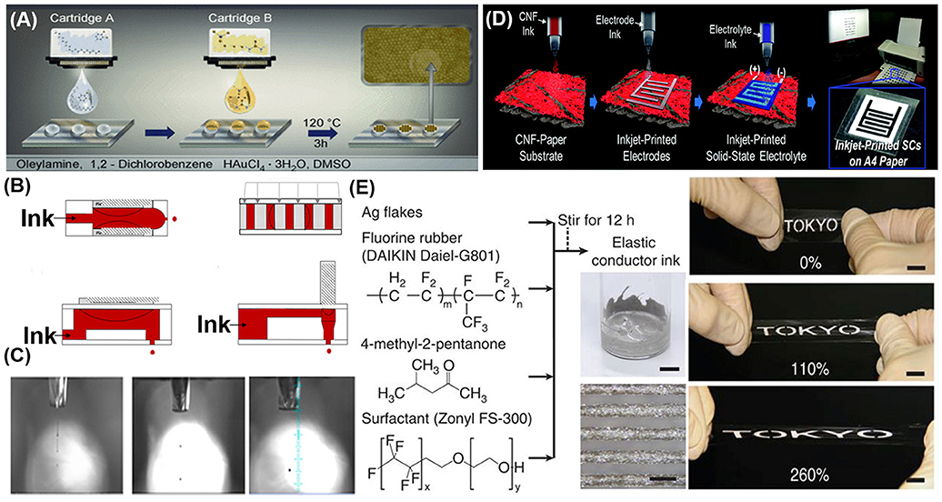
Figure 7. (A) In situ synthesis of the Au nanoparticle in ink printing (Abulikemu et al., 2014). Reproduced with the permission of 1999–2018 John Wiley & Sons. (B) Four types of piezoelectric inkjet nozzles (Eshkalak et al., 2017). Reproduced with the permission of 2018 Elsevier B.V. (C) Drop ejection of the ink (Dankoco et al., 2016). Reproduced with the permission of 2018 Elsevier B.V. (D) Fabrication of supercapacitors with the inkjet printing technique (Choi et al., 2016). Reproduced with the permission of 2016 Royal Society of Chemistry. (E) Fabrication process of elastic ink and printed elastic patterns under a tensile force (Matsuhisa et al., 2015). Reproduced with the permission of 2015 Macmillan Publishers Limited.
Combination of Screen and Inkjet Printing Technologies
For some applications, a single printing technology cannot satisfy the need for a fabrication process, thus, a combination of printing technologies is desirable. The fabrication process of organic thin film transistors on flexible substrates is based on multiple printing technologies, including inkjet, and screen-printing technologies, as it shown in Figure 8A. First, the screen-printing ink used in this experiment was graphene ink, which has a high viscosity of ~70 Pa to prevent excessive spreading out of the substrate. The squeegee was made of silicon and the printed electrodes were exposed to a Xenon lamp to improve the conductivity of the graphene printed electrodes. The channel was deposited by aerosol-jet printing and the gate dielectric was deposited by the inkjet printing technology. Images of a single electrode and of multiple electrodes are shown in Figures 8B,C, respectively. The details of the flexible graphene electrodes are shown in Figures 8D–G. The width and thickness of the printed electrode fabricated by the silicon squeegee, with an opening of 30 μm ~58.2 ± 7 μm and 1.11 ± 0.9 μm, respectively, is illustrated in Figures 8D,E. By combining printing technologies, the advantages of various techniques can be fully applied.
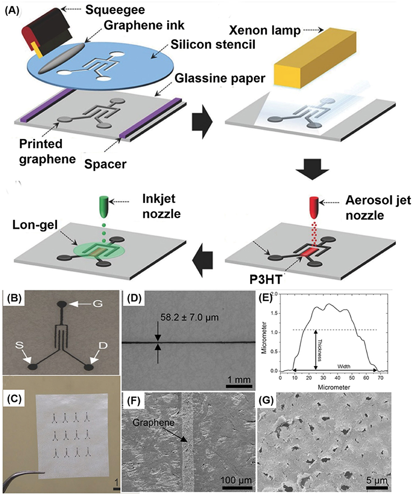
Figure 8. (A) Transistor procedure utilizing screen and inkjet printing technologies. (B) Optical microscopy images of transistors. (C) Optical photograph of the printed transistor array. (D) Optical microscopy image of graphene electrode. (E) Surface profile of the graphene electrode. (F,G) Low and high magnification SEM images of screen-printed graphene electrodes (Hyun et al., 2015b). Reproduced with the permission of 2015 WILEY-VCH Verlag GmbH & Co. KGaA, Weinheim.
Soft Lithography
Soft lithography is an effective method for fabricating patterned electrodes. Stefanie Lochmann et al. reported a novel way of manufacturing electrodes of micro capacitors based on soft lithography (Lochmann et al., 2018). Figure 9A shows the procedure of fabrication. A droplet of the precursor solution was spread over the substrate and the stamp was pressed into the precursor solution. After thermal treatment, the stamp was peeled off, thereby leaving the desired interdigital electrodes on the substrates. Figures 9B,C show the images of the interdigital carbon electrodes. Eduardo et al. reported a novel nanocomposite based on AgNWs, dispersed in poly(methyl methacrylate) with a sheet resistance below 10 Ω sq−1, an acceptable resistance for flexible electrodes (Martínez et al., 2016). The fabricated resistance, based on soft lithography, is shown in Figures 9B,C. The optical images of conductive tracks in the bright field mode and dark field mode are displayed in Figures 9D,E, respectively. The length of the electrode is ~100 μm.
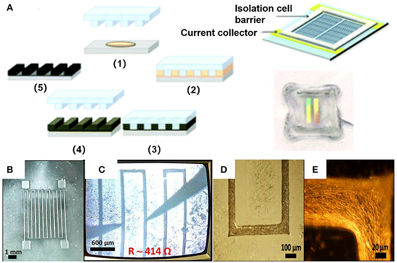
Figure 9. (A) Schematic diagram of the electrodes utilized soft lithography method (Lochmann et al., 2018). Reproduced with the permission of 2018 Royal Society of Chemistry. (B) The optical images of fabricated electrodes (B) Optical images of flexible conductive electrodes. (C) Measurement of conductive trace. Optical images in bright field mode and dark field mode shown in (D,E), respectively (Martínez et al., 2016). Reproduced with the permission of 2016 IOP Publishing Ltd.
The Bottom-Up Technologies of Printed Electrodes
In addition to the physical methods of depositing or printing conductors on substrates, chemical methods are also employed. In contrast to transferring ink onto substrates physically, bottom-up methods involve the chemical reaction that occurs on the surface, strengthening the connection between the electrodes and substrates. Here, two main chemical methods are reviewed.
Polymer-Assisted-Deposition (PAMD)
The full solution processing strategy, polymer-assisted metal deposition (PAMD) is employed for the fabrication of flexible bendable and stretchable metal (especially Cu) electrodes on flexible substrates. Figure 10A is an illustration of PAMD and its applications. The applications of polymer-assist-deposition mentioned, are the same as those shown in Figure 9A. Within polymer-assist-deposition technology, the polymer bonds to the substrates chemically or physically by three main methods: surface-initiated polymerization, in situ free radical polymerization and polymer self-crosslinking, as shown in Figure 10A. The bonds ensure that the polymer layer attaches to the substrates tightly and do not fall out during the steps that follow. The metal thin film on the stretchable substrate that functions as an electrode, is shown at the top of Figure 10A. Working with the matrix-assisted catalytic printing (MACP) method, polymer-assist-deposition demonstrates its ability to fabricate patterned metal electrodes, as shown at the bottom left of Figure 9A. Polymer-assist-deposition is also capable of fabricating 3D stretchable and compressible sponges, as shown at the bottom right of Figure 10A. The process of metal deposition contains three main steps: modification of substrates, immobilization of catalytic moieties and deposition of electrodes. Based on PAMD, metal electrodes, patterned interconnects, and metal sponges can be manufactured. A combination of the PAMD and inspiration from natural vein and vein-like transparent electrodes was reported by Yu et al. (2015a) Figure 10B demonstrates the procedure of depositing Cu on the natural vein. Digital and SEM images of natural veins and vein electrodes are shown in Figures 10C–E, respectively. The transparent electrodes maintain the hierarchical structures of the veins with a thickness of metal Cu ~250 nm. Figure 10F illustrates the feasibility of flexible electrodes by illuminating an array of LED with a bulk resistance of ~4 Ω. Embedded within the substrates, the electrodes fabricated by the means of PAMD possess a greater flexibility and adhesion with the substrates, than the electrodes did using physical methods. In addition, the electrodes also show a high nanoscale resolution and high conductivity over 105 S cm−1. Figure 10G is the optical image transparent electrodes and the natural leaves, showing it high transparency.
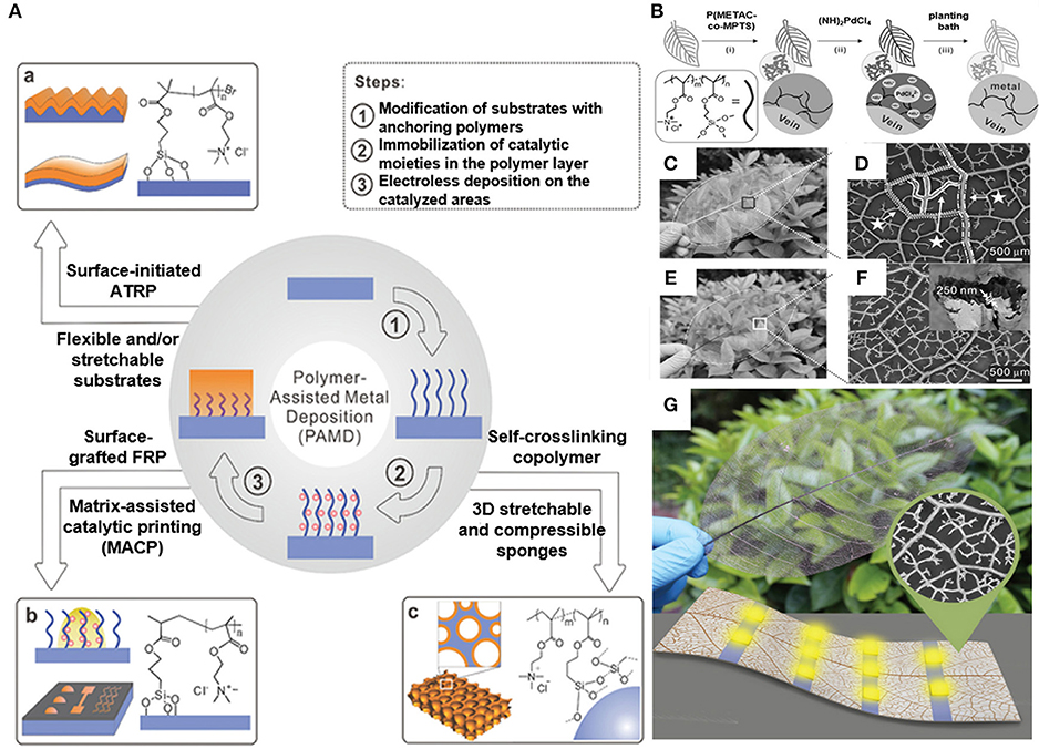
Figure 10. (A) Schematic illustration of polymer-assisted metal deposition and its various applications, including patterned metal electrodes and metal sponges (Yu et al., 2014). Reproduced with the permission of 2014 WILEY-VCH Verlag GmbH & Co. KGaA, Weinheim. (B) Fabrication process of vein-based transparent electrodes. (C,D) SEM images of natural veins. (E,F) SEM images of vein-based transparent electrodes. (G) Optical photography of vein-based electrodes (Yu et al., 2015a). Reproduced with the permission of 1999–2018 John Wiley & Sons, Inc.
Ion-Exchange Technology
As a bottom-up method, the ion-exchange fabrication makes use of the mechanism of replacement reaction between K+ and Ag+ and the reduction of Ag+ with the deposited metal in the desired zone of PI. Figure 11A shows a diagram of flexible Ag electrodes via hydrolysis, ion-exchange, and thermal treatment steps. After the immersion in KOH solution, the surface of polyimide was embedded with K+ ions and then modified with acrylic acid polymers (PAA). Ion-exchanges of K+ into Ag+ are achieved by immersing the substrate in a solution of AgNO3 and NH3·H2O. The patterned Ag electrodes are obtained in two different ways. First, the KOH modified PI substrates are pasted flatly onto the paper and inkjet printing, with carbon ink, is used as the mask for the reduction of Ag+ ions into silver atoms in a H2O2 solution. Secondly, the inkjet printed PI films are thermally cured in an air oven. Figure 11B shows an optical image of flexible Ag electrode arrays on PI. The ability to be printed in an array can accomplish numerous functions. One single interdigital electrode cell is comparable to the size of a coin. Figures 11C,D show the different morphology of electrodes before and after Au coating. Besides the relatively simple fabrication steps mentioned, the cost of the fabrication process is low and does not require sophisticated devices and an ultra-clean environment. Additionally, the fabrication process produces no air or water pollution and has a low power consumption. One step mask technology simplifies procedures of patterned electrodes, while the conductivity and thickness of the electrodes can be controlled by adjusting the time of the ion-exchange reaction and the concentrations of the KOH and H2O2 solution employed during the procedure. Similarly, in polymer-assist-deposition, the adhesion between the electrodes and flexible PI substrate is strong. The full-solution process eliminates pollution possibilities of air; hence, the formed mental electrodes are compact. Further, the ion-exchange reaction only takes place on the surface of the PI substrates, while the middle part of the PI substrates remain unaffected because of its mechanical strength and stability. On the basis of printed electrodes, graphene/graphene oxide pressure sensitive film arrays are placed on the PI substrates, thereby fabricating an advanced electric blanket shown in Figures 11E,F. These pressure sensors operate at a constant voltage. When the sensor experiences an exerted force, their resistance decreases, and the current increases. The increasing current and pressure could lead to heat generation. The infrared images reflect the temperature of the object. With loaded pressure, the corresponding infrared image is displayed in Figure 11G, illustrating the possibility of future application. Identical to the PAMD technology, the ion-exchange method fundamentally solves the problem of weak connections between electrodes and substrates while maintaining good conductivity and high solution.
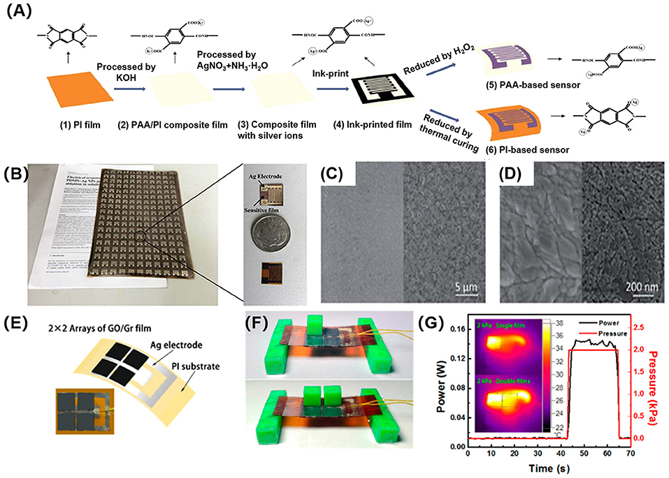
Figure 11. (A) Procedure of fabricating humidity sensors with Ag interdigitated electrodes using the ion-exchange method. (B) Optical photography of an Ag interdigitated electrode array (Yang et al., 2015). Reproduced with the permission of 2015 Elsevier B.V. (C,D) SEM images of Ag film before and after Au coating. (E) Graphene/graphene oxide resistance sensitive film array on Ag electrodes. (F,G) Demonstration of an advanced electric blanket and thermal infrared images with loading pressure (Liu et al., 2017). Reproduced with the permission of the American Chemical Society.
Based on the traditional technology of Ag deposition on the substrate, composites of Ag and nanotubes can also be obtained to improve the performance of supercapacitors. Figure 12A shows a flow chart of micro-supercapacitors with Ag/multi wall nanotubes (MWNT) as interdigital electrodes. A clean PI substrate was immersed in a KOH solution and then covered with a photosensitive film. With a patterned inkjet printed electrode film as a mask, the prepared composite of PI and photosensitive film was exposed to air and then immersed in NaCO3 to form the patterned electrodes on the film. Ion-exchanges take place when the mask-protected PI film is soaked in Ag(NH3)2+ and an H2O2 solution stepwise. The PI and Ag electrodes are then dipped into the MWNT solution and air dried. The patterned photosensitive film is removed, leaving the interdigital electrodes of Ag/MWNT on PI. Figures 12B,C are optical images of the fabricated electrodes on the PI being bent. After being bent, the electrodes stuck to the substrate without a gap. As shown in the SEM image in Figure 12D, the electrodes were embedded in the surface of the substrate, leading to good bending reliability while the profile of the electrodes was also clear and well defined. Figure 12E shows an optical microscopy image of the electrodes. The patterns of the electrode are well defined without deformation and the width is ~ 100 μm. In the SEM image of the Ag micro current collector fabricated with the ion-exchange method shown in Figure 12F, the thickness measures ~200 nm. Figure 12G illustrates the comparison of conductivity among the bulk Ag, fabricated Ag film using the ion-exchange method and WMNTs. The measured conductivity of the Ag film is ~1.68 × 10⁵s cm−1, which is much higher than that of WMNTs and comparable with that of the Ag bulk. Based on the details discussed above, the technical parameters of different technologies are listed in Table 1.
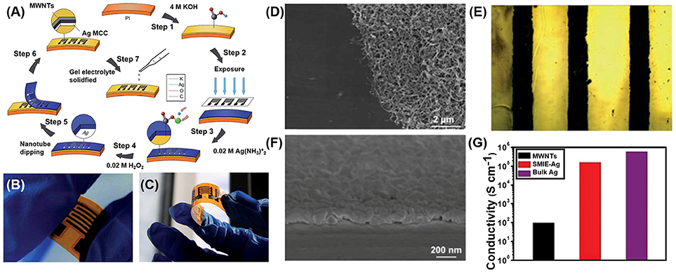
Figure 12. (A) A flow chart of micro-supercapacitors using surface metallization via the ion-exchange method. (B,C) Optical images of supercapacitors with printed electrodes. (D) SEM image of the boundary of the substrate and electrode. (E) The optical image of electrodes of multiwall carbon nanotubes. (F) SEM image of metal current collector. (G) Conductivity comparison among various materials as electrodes (Yu et al., 2015b). Reproduced with the permission of 2015 Royal Society of Chemistry.
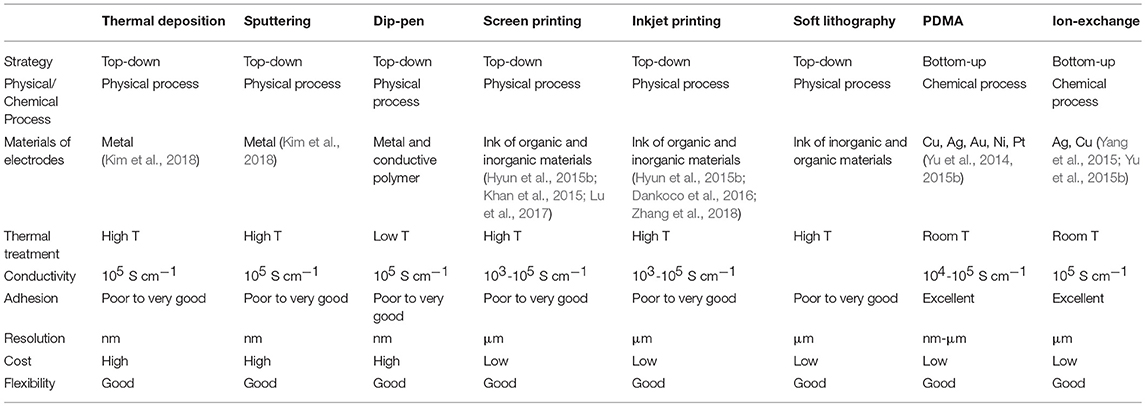
Table 1. Technical specifications of flexible electrode technologies.
Summary
The fabrication of flexible electrodes applied to flexible electronics, can be classified into two fabrication process categories: top-down and bottom-up. Top down technology uses physical procedures to deposit organic and inorganic materials onto the substrate directly. The conventional methods possess a high solution and high conductivity. For screen and inkjet printing technologies, the one-step transfer of functional ink onto a substrate saves on costs, whereas bottom-up technologies, including PAMD and ion-exchange, produces an obvious advantage of strong adhesion between metal and substrates at their surface, as a consequence of their interpenetration.
Perspective
Although existing fabrication technologies promise to meet the requirements of flexible electrodes utilized in flexible electronic devices, challenges remain to obtain a low-cost, high-solution, high-throughput, and high-conductivity manufacturing process.
High temperature treatment in conventional fabrication technologies. In top-down methods of the fabrication process, physical evaporation and deposition requires the metal to evaporate in order to be deposited, and the printing technology requires a sintering process to improve conductivity. Among all the procedures mentioned above, thermal treatment is indispensable, in other words, the cost is relatively higher for thermal treatment than the cost for bottom-up methods. Obtaining a low cost method therefore remains a great challenge for these technologies.
The choice and synthesis of ink in screen and inkjet printing technologies. The ink plays an important role in printing technologies because of its responsibility of solution, conductivity, and adhesion to the substrates. Many organic and inorganic materials have been used to fabricate flexible electrodes, and the improvements in high solution and high conductivity are future goals.
The breakthrough in metal limitations. Bottom-up technologies that take advantage of a catalyst or reduction reaction to embed metal into the surface of substrate surface, are limited by the finite choice of metals. Various metals need to be deposited on substrates to explore their corresponding performances.
The compatibility with roll-to-roll technology. Mass production is the terminal target of printed electronics, which feature low cost and high output, thus, compatibility with roll-to-roll technology are significant. Both the top-down and bottom-up technologies should take mass production compatibility into consideration.
Author Contributions
XW and JZ conceived and designed structure of the review. QuL, JZ, QiL, GL, XT, ZL, and FQ wrote the manuscript. All authors contributed to the discussion and commented on the manuscript.
Conflict of Interest Statement
The authors declare that the research was conducted in the absence of any commercial or financial relationships that could be construed as a potential conflict of interest.
Acknowledgments
We would like to acknowledge support from the NSFC (11504111 and 61574060), the Projects of Science and Technology Commission of Shanghai Municipality Grant (5JC1401800 and 14DZ2260800), the Program for Professor of Special Appointment (Eastern Scholar), and the Shanghai Rising-Star Program (17QA1401400), as well as the Fundamental Research Funds for the Central Universities.
References
Abulikemu, M., Da'as, E. H., Haverinen, H., Cha, D., Malik, M. A., and Jabbour, G. E. (2014). In situ synthesis of self-assembled gold nanoparticles on glass or silicon substrates through reactive inkjet printing. Angew. Chem. 53, 420. doi: 10.1002/anie.201308429
Bae, S., Kim, H., Lee, Y., Xu, X., Park, J. S., Zheng, Y., et al. (2010). Roll-to-roll production of 30-inch graphene films for transparent electrodes. Nat. Nanotechnol. 5:574–578. doi: 10.1038/nnano.2010.132
Bariya, M., Shahpar, Z., Park, H., Sun, J., Jung, Y., Gao, W., et al. (2018). Roll-to-roll gravure printed electrochemical sensors for wearable and medical devices. ACS Nano 12, 6978–6987. doi: 10.1021/acsnano.8b02505
Bermúdez, G. S. C., Karnaushenko, D. D., Karnaushenko, D., Lebanov, A., Bischoff, L., Kaltenbrunner, M., et al. (2018). Magnetosensitive E-skins with directional perception for augmented reality. Sci. Adv. 4:eaao2623. doi: 10.1126/sciadv.aao2623
Byun, J., Lee, Y., Yoon, J., Lee, B., Oh, E., Chung, S., et al. (2018). Electronic skins for soft, compact, reversible assembly of wirelessly activated fully soft robots. Sci Reb. 3:eaas9020. doi: 10.1126/scirobotics.aas9020
Chen, L., Wei, X., Zhou, X., Xie, Z., Li, K., Ruan, Q., et al. (2017). Large-area patterning of metal nanostructures by dip-pen nanodisplacement lithography for optical applications. Small 13:1702003. doi: 10.1002/smll.201702003
Choi, K.-H., Yoo, J., Lee, C. K., and Lee, S.-Y. (2016). All-inkjet-printed, solid-state flexible supercapacitors on paper. Energy Environ. Sci. 9 :2812. doi: 10.1039/c6ee00966b
Chu, Y., Zhong, J., Liu, H., Ma, Y., Liu, N., Song, Y., et al. (2018). Human pulse diagnosis for medical assessments using a wearable piezoelectret sensing system. Adv. Funct. Mater. 28:1803413. doi: 10.1002/adfm.201803413
Cronin, S. D., Sabolsky, K., Sabolsky, E. M., and Sierros, K. A. (2014). Dip pen nanolithography and transfer of zno patterns on plastics for large-area flexible optoelectronic applications. Thin Solid Films 552, 50–55. doi: 10.1016/j.tsf.2013.12.018
Dankoco, M. D., Tesfay, G. Y., Benevent, E., and Bendahan, M. (2016). Temperature sensor realized by inkjet printing process on flexible substrate. Mater. Sci. Eng. B 205, 1–5. doi: 10.1016/j.mseb.2015.11.003
Eshkalak, S. K., Chinnappan, A., Jayathilaka, W. A. D. M., Khatibzadeh, M., Kowsari, E., and Ramakrishna, S. (2017). A review on inkjet printing of Cnt composites for smart. Applications 9, 372–386. doi: 10.1016/j.apmt.2017.09.003
Gao, W., Emaminejad, S., Nyein, H. Y. Y., Challa, S., Chen, K., Peck, A., et al. (2016). Fully integrated wearable sensor arrays for multiplexed in situ perspiration analysis. Nature 529, 509–514. doi: 10.1038/nature16521
Hyun, W. J., Secor, E. B., Hersam, M. C., Frisbie, C. D., and Francis, L. F. (2015a). High-resolution patterning of graphene by screen printing with a silicon stencil for highly flexible printed electronics. Adv. Mater. 27, 109–115. doi: 10.1002/adma.201404133
Hyun, W. J., Secor, E. B., Rojas, G. A., Hersam, M. C., Francis, L. F., and Frisbie, C. D. (2015b). All-printed, foldable organic thin-film transistors on glassine paper. Adv. Mater. 27, 7058–7064. doi: 10.1002/adma.201503478
Jang, K. I., Chung, H. U., Xu, S., Lee, C. H., Luan, H., Jeong, J., et al. (2015). Soft network composite materials with deterministic and bio-inspired designs. Nat. Commun. 6 :6566. doi: 10.1038/ncomms7566
Jang, K. I., Han, S. Y., Xu, S., Mathewson, K. E., Zhang, Y., Jeong, J. W., et al. (2014). Rugged and breathable forms of stretchable electronics with adherent composite substrates for transcutaneous monitoring. Nat. Commun. 5:4779. doi: 10.1038/ncomms5779
Khan, S., Tinku, S., Lorenzelli, L., and Dahiya, R. S. (2015). Flexible tactile sensors using screen-printed P(Vdf-Trfe) and Mwcnt/Pdms composites. IEEE Sens. J. 15, 3146–3155. doi: 10.1109/JSEN.2014.2368989
Kim, Y., Chortos, A., Xu, W., Liu, Y., Oh, J. Y., Son, D., et al. (2018). A bioinspired flexible organic artificial afferent nerve. Science 360, 998–1003. doi: 10.1126/science.aao0098
Lee, H., Song, C., Hong, Y. S., Kim, M. S., Cho, H. R., Kang, T., et al. (2017). Wearable/disposable sweat-based glucose monitoring device with multistage transdermal drug delivery module. Sci. Adv. 3:e1601314. doi: 10.1126/sciadv.1601314
Lee, S.-S., Choi, K.-H., Kim, S.-H., and Lee, S.-Y. (2018). Wearable supercapacitors printed on garments. Adv. Funct. Mater. 28:1705571. doi: 10.1002/adfm.201705571
Leung, S. F., Ho, K. T., Kung, P. K., Hsiao, V. K. S., Alshareef, H. N., Wang, Z. L., et al. (2018). A self-powered and flexible organometallic halide perovskite photodetector with very high detectivity. Adv. Mater. 30:1704611. doi: 10.1002/adma.201704611
Li, J., Lu, W., Yan, Y., and Chou, T.-W. (2017). High performance solid-state flexible supercapacitor based on Fe3o4/Carbon Nanotube/Polyaniline ternary films. J. Mater. Chem. 5, 11271–112177. doi: 10.1039/c7ta02008b
Li, W., Chen, M., Jin, H., Liu, J., Zeng, Z., Zhang, H., et al. (2017). Effective fabrication of flexible negative refractive index metamaterials using a simple screen printing method. J. Mater. Chem. C 5, 5378–5386. doi: 10.1039/c7tc01091e
Lin, C. C., Sun, D. S., Lin, Y. L., Tsai, T. T., Cheng, C., Sun, W. H., et al. (2017). A flexible and miniaturized hair dye based photodetector via chemiluminescence pathway. Biosens. Bioelectron. 90, 349–355. doi: 10.1016/j.bios.2016.12.011
Lin, S., Bai, X., Wang, H., Wang, H., Song, J., Huang, K., et al. (2017). Roll-to-roll production of transparent silver-nanofiber-network electrodes for flexible electrochromic smart windows. Adv. Mater. 29:1703238. doi: 10.1002/adma.201703238
Liu, S., Wu, X., Zhang, D., Guo, C., Wang, P., Hu, W., et al. (2017). Ultrafast dynamic pressure sensors based on graphene hybrid structure. ACS Appl. Mater. Interfaces 9, 24148–24154. doi: 10.1021/acsami.7b07311
Lochmann, S., Grothe, J., Eckhardt, K., Leistenschneider, D., Borchardt, L., and Kaskel, S. (2018). Nanoimprint lithography of nanoporous carbon materials for micro-supercapacitor architectures. Nanoscale 10, 10109–10115. doi: 10.1039/c8nr01535j
Lou, Z., Chen, S., Wang, L., Shi, R., Li, L., Jiang, K., et al. (2017). Ultrasensitive and ultraflexible e-skins with dual functionalities for wearable electronics. Nano Energy 38, 28–35. doi: 10.1016/j.nanoen.2017.05.024
Lu, Q., Liu, L., Yang, S., Liu, J., Tian, Q., Yao, W., et al. (2017). Facile synthesis of amorphous Feooh/Mno 2 composites as screen-printed electrode materials for all-printed solid-state flexible supercapacitors. J. Power Sources 361, 31–38. doi: 10.1016/j.jpowsour.2017.06.065
Martínez, E. D., Lohr, J. H., Sirena, M., Sánchez, R. D., and Pastoriza, H. (2016). Silver nanowires in poly(Methyl Methacrylate) as a conductive nanocomposite for microfabrication. Flexible Printed Electron. 1:035003. doi: 10.1088/2058-8585/1/3/035003
Matsuhisa, N., Kaltenbrunner, M., Yokota, T., Jinno, H., Kuribara, K., Sekitani, T., et al. (2015). Printable elastic conductors with a high conductivity for electronic textile applications. Nat. Commun. 6:7461. doi: 10.1038/ncomms8461
Navaraj, W. T., Gupta, S., Lorenzelli, L., and Dahiya, R. (2018). Wafer scale transfer of ultrathin silicon chips on flexible substrates for high performance bendable systems. Adv. Electron. Mater. 4, 1700277. doi: 10.1002/aelm.201700277
Pan, L., Liu, G., Shi, W., Shang, J., Leow, W. R., Liu, Y., et al. (2018). Mechano-regulated metal-organic framework nanofilm for ultrasensitive and anti-jamming strain sensing. Nat. Commun. 9:3813. doi: 10.1038/s41467-018-06079-3
Park, S., Heo, S. W., Lee, W., Inoue, D., Jiang, Z., Yu, K., et al. (2018). Self-powered ultra-flexible electronics via nano-grating-patterned organic photovoltaics. Nature 561, 516–521. doi: 10.1038/s41586-018-0536-x
Sahu, B. B., Long, W., and Han, J. G. (2018). Highly conductive flexible ultra thin ito nanoclusters prepared by 3-D confined magnetron sputtering at a low temperature. Scr. Mater. 149, 98–102. doi: 10.1016/j.scriptamat.2018.02.018
Son, D., Lee, J., Qiao, S., Ghaffari, R., Kim, J., Lee, J. E., et al. (2014). Multifunctional wearable devices for diagnosis and therapy of movement disorders. Nat. Nanotechnol. 9, 397–404. doi: 10.1038/nnano.2014.38
Wang, C., Wu, X., Ma, Y., Mu, G., Li, Y., Luo, C., et al. (2018). Metallic few-layered Vse 2 nanosheets: high two-dimensional conductivity for flexible in-plane solid-state supercapacitors. J. Mater. Chem. 6, 8299–8306. doi: 10.1039/C8TA00089A
Wang, C., Zhao, D., Yu, Y., Shrestha, N., Grice, C. R., Liao, W., et al. (2017). Compositional and morphological engineering of mixed cation perovskite films for highly efficient planar and flexible solar cells with reduced hysteresis. Nano Energy 35, 223–232. doi: 10.1016/j.nanoen.2017.03.048
Wang, M., Li, Z., Wang, C., Zhao, R., Li, C., Guo, D., et al. (2017). Novel Core&Ndash;Shell Feof/Ni(Oh)2 hierarchical nanostructure for all-solid-state flexible supercapacitors with enhanced performance. Adv. Funct. Mater. 27:1701014. doi: 10.1002/adfm.201701014
Wang, X., Liu, Z., and Zhang, T. (2017). Flexible sensing electronics for wearable/attachable health monitoring. Small 13:1602790. doi: 10.1002/smll.201602790
Wisser, F. M., Schumm, B., Mondin, G., Grothe, J., and Kaskel, S. (2015). Precursor strategies for metallic nano- and micropatterns using soft lithography. J. Mater. Chem. C 3, 2717–2731. doi: 10.1039/c4tc02418d
Wixforth, A., Maedler, C., Graaf, H., Chada, S., Yan, M., and La Rosa, A. (2009). Nanostructure formation driven by local protonation of polymer thin. Films 7364:736409. doi: 10.1117/12.821466
Wu, W. (2017). Inorganic nanomaterials for printed electronics: a review. Nanoscale 9, 7342 −7372. doi: 10.1039/c7nr01604b
Xi, J., Wu, Z., Jiao, B., Dong, H., Ran, C., Piao, C., et al. (2017). Multichannel interdiffusion driven fasni3 film formation using aqueous hybrid salt/polymer solutions toward flexible lead-free perovskite solar cells. Adv. Mater. 29:1606964. doi: 10.1002/adma.201606964
Xu, J., Zhong, C., and Fu, C. (2007). Novel Method for Printing High-Quality Metal, Wires Shanghai, SPIE Newsroom. doi: 10.1117/2.1200712.0969
Yang, T., Yu, Y. Z., Zhu, L. S., Wu, X., Wang, X. H., and Zhang, J. (2015). Fabrication of silver interdigitated electrodes on polyimide films via surface modification and ion-exchange technique and its flexible humidity sensor application. Sens. Actuators. B 208, 327–333. doi: 10.1016/j.snb.2014.11.043
Yu, Y., Yan, C., and Zheng, Z. (2014). Polymer-assisted metal deposition (pamd): a full-solution strategy for flexible, stretchable, compressible, and wearable metal conductors. Adv. Mater. 26, 5508–5516. doi: 10.1002/adma.201305558
Yu, Y., Zhang, J., Wu, X., and Zhu, Z. (2015a). Facile Ion-exchange synthesis of silver films as flexible current collectors for micro-supercapacitors. J. Mater. Chem. 3, 21009–21015. doi: 10.1039/c5ta04913j
Yu, Y., Zhang, Y., Li, K., Yan, C., and Zheng, Z. (2015b). Bio-inspired chemical fabrication of stretchable transparent electrodes. Small 11, 3444–3449. doi: 10.1002/smll.201500529
Zhang, F., Zang, Y., Huang, D., Di, C. A., and Zhu, D. (2015). Flexible and self-powered temperature-pressure dual-parameter sensors using microstructure-frame-supported organic thermoelectric materials. Nat. Commun. 6:8356. doi: 10.1038/ncomms9356
Zhang, X., Santra, P. K., Tian, L., Johansson, M. B., Rensmo, H., and Johansson, E. M. J. (2017). Highly efficient flexible quantum dot solar cells with improved electron extraction using mgzno nanocrystals. ACS Nano 11, 8478–8487. doi: 10.1021/acsnano.7b04332
Keywords: printed electrodes, flexible devices, electronic devices, metal nanomaterials, ion-exchange technology
Citation: Li Q, Zhang J, Li Q, Li G, Tian X, Luo Z, Qiao F, Wu X and Zhang J (2019) Review of Printed Electrodes for Flexible Devices. Front. Mater. 5:77. doi: 10.3389/fmats.2018.00077
Received: 30 October 2018; Accepted: 11 December 2018;
Published: 30 January 2019.
Edited by:
Xiangheng Xiao, Wuhan University, ChinaReviewed by:
Weida Hu, Shanghai Institute of Technology, ChinaWenzhong Bao, Fudan University, China
Copyright © 2019 Li, Zhang, Li, Li, Tian, Luo, Qiao, Wu and Zhang. This is an open-access article distributed under the terms of the Creative Commons Attribution License (CC BY). The use, distribution or reproduction in other forums is permitted, provided the original author(s) and the copyright owner(s) are credited and that the original publication in this journal is cited, in accordance with accepted academic practice. No use, distribution or reproduction is permitted which does not comply with these terms.
*Correspondence: Xing Wu, xwu@ee.ecnu.edu.cn
Jian Zhang, jzhang@ee.ecnu.edu.cn
†These authors have contributed equally to this work