Modeling of temperature dependence of Λ-graded InGaN solar cells for both strained and relaxed features
 Mirsaeid Sarollahi1
  Mohammad Zamani-Alavijeh2
  Manal A. Aldawsari3 Rohith Allaparthi1 Md Helal Uddin Maruf4
  Malak Refaei4
  Reem Alhelais4 Yuriy I. Mazur5
  Morgan E. Ware1,3,4,5*
- 1Electrical Engineering Department, 3217 Bell Engineering Center, University of Arkansas, Fayetteville, AR, United States
- 2Physics Department, University of Arkansas, Fayetteville, AR, United States
- 3Microelectronics-Photonics Program, University of Arkansas, Fayetteville, AR, United States
- 4Material Science and Engineering, University of Arkansas, Fayetteville, AR, United States
- 5Institute for Nanoscience and Engineering, Fayetteville, AR, United States
The temperature dependence of Λ-graded InGaN solar cells is studied through simulation using nextnano software. Λ-Graded structures have been designed by increasing and then decreasing the indium composition in epitaxial InGaN layers. Due to polarization doping, layers of p-type and n-type doping arise without the need for impurity doping. Different individual structures are designed by varying the indium alloy profile from GaN to maximum indium concentrations,
Introduction
Ternary alloys of group III-N materials have great potential to be used in photovoltaic devices due to spectacular properties such as high thermal conductivity, high optical absorption (∼105 cm−1), and high radiation resistance (Nakamura et al., 1995; Nakamura et al., 1996; Pozina et al., 2000; Bhuiyan et al., 2012; Kucukgok et al., 2016; Kazazis et al., 2018). Additionally, these materials have direct band gaps (Kazazis et al., 2018) which creates strong optical transitions for charge carriers between the conduction band (CB) and valence band (VB). Also, they have a tunable band gap, which covers almost the whole range of the visible solar spectrum from UV up to infrared (Bhuiyan et al., 2012; David and Grundmann, 2010; Routray and Lenka, 2018; Belghouthi and Aillerie, 2019; Cheriton et al., 2020). Several groups have reported that modeling efforts aimed at describing the solar cell parameters of devices made from InGaN alloys. For example, the solar efficiency for a single-junction
In another report, a quantum well (QW) LED with graded InGaN QWs was studied, experimentally and theoretically. The advantages of using graded structures in comparison with fixed compositions of QWs were reported. A graded structure was determined, through simulations, to reduce carrier densities such that Auger recombination (which is the main cause of the lost efficiency through non-radiative recombination) was decreased. Graded structures also decrease polarization-induced interface charge density, which also contributes to efficiency loss, from approximately 0.54 × 10¹⁷ m−2 to 0.3 × 10¹⁷ m−2. Moreover, the quantum-confined stark effect, which is significant in QWs, is much less significant in the graded structure. In QWs, this acts to increase the carrier lifetime, which dramatically increases the probability of capture by the contacts, but at the same time, it does decrease the absorptivity of the QW region. Additionally, graded structures increase the overlap of electron and hole wavefunctions, which also acts to increase the absorption. The external quantum efficiency (EQE) for the graded structure shows 39.23%, which is higher than that of the QW structure at 31.83%. At the end, they reported the output for the graded structure to be ∼150 A/cm2 injection current, which is almost 30% higher than that of the QW device (Zhang et al., 2014).
In the present work, the designed structure is a Λ-shaped graded structure in which the indium composition is linearly changed vs. position in the structure. Polarization doping plays a crucial role in the graded structure to reach high levels of doping, without using additional impurities in the lattice (LeGoues et al., 1992) as growing p-type InGaN alloys is one of the main technical challenges (Obloh et al., 1998; Van de Walle and Segev, 2007; Brochen et al., 2013; Ra and Lee, 2019; Narita et al., 2020). The graded structure provides polarization doping which creates p- and n-type layers. This is the result of changing the built-in polarization, creating a space charge,
Here, we present simulations of Λ-graded InGaN solar cells. In addition, the effects of temperature and strain are studied using nextnano software. The graded structure consists of a symmetric double InGaN-graded layer in which the indium composition linearly increases from GaN to a maximum value,
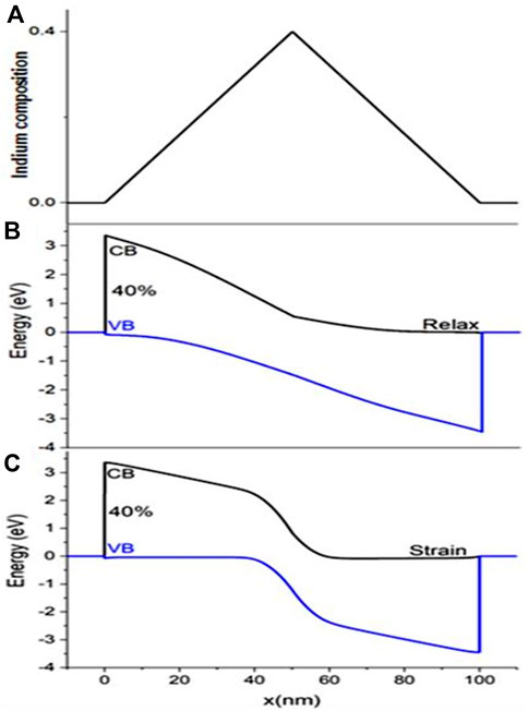
FIGURE 1. (A) Indium composition vs. position. (B) Energy band diagram vs. position (fully relaxed). (C) Energy band diagram vs. position (fully strained) for the
nextnano simulation and strategy
nextnano software, consisting of two different versions, nextnano3 and nextnano+, was used to simulate solar cell parameters. Within nextnano, we use a single-band, effective-mass approximation to calculate the band structure. Also, in order to obtain the light IV plot, the generation rates for each layer of the material must be calculated. In order to incorporate the generation rate of a varying alloy composition, the graded structure is approximated as a step-graded structure due to the fact that nextnano is limited to simulating the generation rate of a single composition at once. The generation rate for each individual layer is calculated using nextnano3, and then the layers are combined and imported into nextnano+ in order to calculate the light IV curve for the entire structure. The solar cell parameters such as the open circuit voltage,
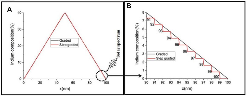
FIGURE 2. (A) Changing the graded structure to step-graded structure for calculating the generation rate in nextnano3. Direction of the solar spectrum and hitting position to the structure is shown as well. (B) Zoom in for 90–100 nm to show converting graded to step-graded structure in which the number of each layer is given in addition to the layer when light passes through the structure.
In order to calculate the generation rate within each layer, the intensity of light incident on that layer and the absorption coefficient of that layer are required. The parameterization of the absorption coefficients is described as follows: the light intensity at each layer is determined by the exponential loss of intensity from the layer directly above, using the full solar intensity spectrum (AM 1.5G) as the source incident on the external surface of the device. For example, using 100 layers with the 100th layer facing the Sun, the light transmitted through the top layer and incident on the 99th layer would be given by
In this work, the effects of temperature on graded InGaN solar cells are studied, with the primary effect being to decrease the band gap as the temperature increases (O’Donnell and Chen, 1991; Wu et al., 2003; Cho et al., 2020). Solar cell parameters such as short-circuit current density, open-circuit voltage, efficiency, and fill factor are all therefore affected by changing the temperature (Belghouthi and Aillerie, 2019; Adeeb et al., 2019; Boney et al., 2012). For each structure, the solar cell properties were studied between 100 K and 800 K. For simple homojunction solar cell structures, it is generally understood that there is a direct correlation between the band gap and the open-circuit voltage (Green, 1998; Blakesley and Neher, 2011; Nelson, 2003). However, the inverse is true for the short-circuit current density,
Strain: impact on device performance
Due to the 11% lattice mismatch between InN and GaN, InGaN structures grown on GaN substrates result in a significant strain. This strain generally manifests a decrease in the band gap, similar to the increase in temperature. Therefore, all the results of changing the temperature and thus changing the solar cell properties through the change in the band gap are similarly studied due to the induced strain in the films including the absorption coefficient and the resulting generation (Park and Chuang, 1999; Romanov et al., 2006; Masui et al., 2008; Azize and Palacios, 2010; Dreyer et al., 2013; Birner et al., 2006; Wierer et al., 2010; Golam Sarwar and Myers, 2012; Belghouthi et al., 2016). In this work, fully strained to GaN and bulk-relaxed lattices were considered. The true experimental realization of these structures is expected to fall between these two extremes.
nextnano software simulates the band structure in the envelope function approximation, using a single-band effective-mass approach (Nextnano, 2021). The electron motion is then determined by the one-electron Hamiltonian method, while multi-body effects are considered negligible (Birner et al., 2006).
The effect of temperature on the energy band gap was calculated between 100 K and 800 K, which is shown in Figures 3A,B, as functions of composition for the strained and relaxed conditions, respectively. Generally, as expected, the band gap is found to decrease with the increase in temperature. Somewhat surprisingly, though, we see that the band gap energy is predicted to be negative for InxGa1-xN, strained to GaN with x >∼90%. This high amount of strain would be difficult to pseudomorphically achieve and maintain in a single-composition thin film. However, within a graded composition structure, the localized strain can be much higher. In what follows, regarding the strained graded structures, we generally limit our discussion to x <∼90% in order to avoid the case where a solar cell has a negative band gap as this is not currently well defined. For the relaxed graded structures, we allow the composition to vary all the way to 100%, that is, pure InN.
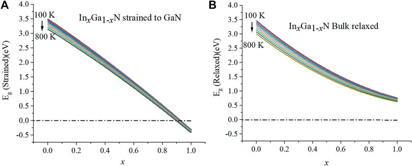
FIGURE 3. Temperature dependence of the energy band gap under the (A) strained condition and (B) relaxed condition (100–800 K).
For the base of the bulk relaxed band gap at low temperature, Eg, nextnano essentially uses Vegard’s law to extrapolate between two components of an alloy with some associated bowing parameters. For InxGa1-xN, this looks like:
where b is the bowing parameter. Different values have been reported for this bowing parameter. Shahab N. Alam et al. presented a review for bowing parameters in the group III-N ternary alloys. For InGaN, these values ranged between 1.4 and 3 eV (Kuo et al., 2001; Moret et al., 2009; Pelá et al., 2011; Alam et al., 2020). Additionally, there have been some reports which indicate that the bowing parameter has some compositional dependence (Caro et al., 2013; Moses et al., 2011), and some which claim no compositional dependence (Nawaz and Ahmad, 2012; Feng et al., 2013; Mesrane et al., 2015). We use the value for the bowing parameter given in the nextnano Material database, b = 1.4 as a reasonable approximation (Vurgaftman et al., 2001; Wu et al., 2002; Vurgaftman and Meyer, 2003). At the same time, other bowing parameters may be possible, but we perform our calculations using this single value in order to learn the general response of the system. Any result which is dependent on the bowing is by its nature a second-order effect and should only minimally affect the present results.
In order to perform the two-step simulation that we have performed, that is, to calculate the generation rates in one software package and then import them to another, we required a full set of analytical relationships for the band gap values of all InGaN alloys at all temperatures. The band gap values were then used to determine the absorption coefficients, analytically, at each temperature. So, first, the band gaps as functions of composition, as shown in Figure 2, were fit to second-order polynomials for each temperature as follows (Sarollahi et al., 2022):
The fitting was carried out in each individual temperature, for which the numbers are given in Table 1.

TABLE 1. Parameters for energy gap under strained and relaxed conditions in different temperatures.
It is seen that
TABLE 2. Parameters for
The absorption coefficient for InGaN can be generally represented as follows (Brown et al., 2010; Belghouthi et al., 2015; Giannoccaro et al., 2016):
where E is the incoming photon energy given in eV and a and b are dimensionless fitting parameters. Belghouthi and Aillerie (2019); Belghouthi et al. (2016); and Belghouthi et al. (2015) determined experimentally a(x) and b(x) over the entire composition range to be
Our goal is to reformulate the absorption coefficients to be the functions of band gap over the entire range of alloys. Once this calculation has been performed, Eq. 5 can be converted to functions of the band gap energies under strained and relaxed conditions by plotting and fitting the parameters in each individual temperature, a and b, as functions of the strained band gap energy under strain and relax conditions with respect to the GaN lattice constant,
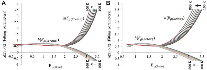
FIGURE 4. Fitting parameter for the absorption coefficients for (A) InGaN strained to GaN and (B) bulk relaxed InGaN at different temperatures.
The best fits for both cases are derived by
Under the strained condition, these parameters as functions of temperature are presented in Tables 3, 4, respectively.
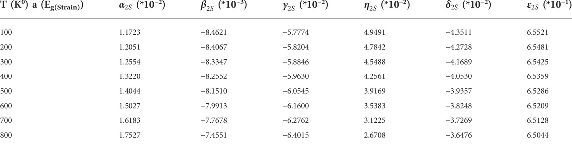
TABLE 3. Fitting parameters for “a” the under strained condition at different temperatures.
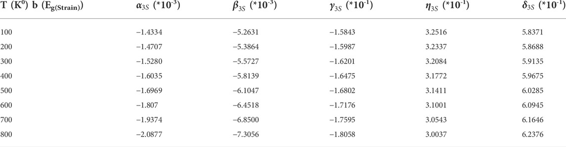
TABLE 4. Fitting parameters for “b” under the strained condition at different temperatures.
Now, again all parameters are fit to a fourth-order polynomial in temperature given by d4T4+ d3T3+ d2T2+ d1T1+ d0. The resulting fitting parameters are shown in Table 5.
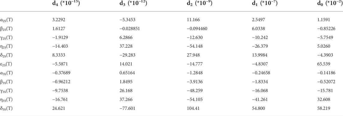
TABLE 5. Fitting parameters for
The same procedure is performed for the relaxed structure. The absorption coefficient parameters, a and b, are fit as functions of T and the relaxed band gap,
with fitting coefficients given in Tables 6, 7.
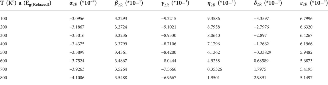
TABLE 6. Fitting parameters for “a” under the relaxed condition at different temperatures.
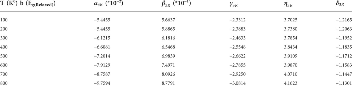
TABLE 7. Fitting parameters for “b” under the relaxed condition at different temperatures.
Now, again all parameters for the relaxed condition as functions of temperatures are fit with a fourth-order polynomial, e4T4+ e3T3+ e2T2+ e1T1+ e0, with coefficients given in Table 8.
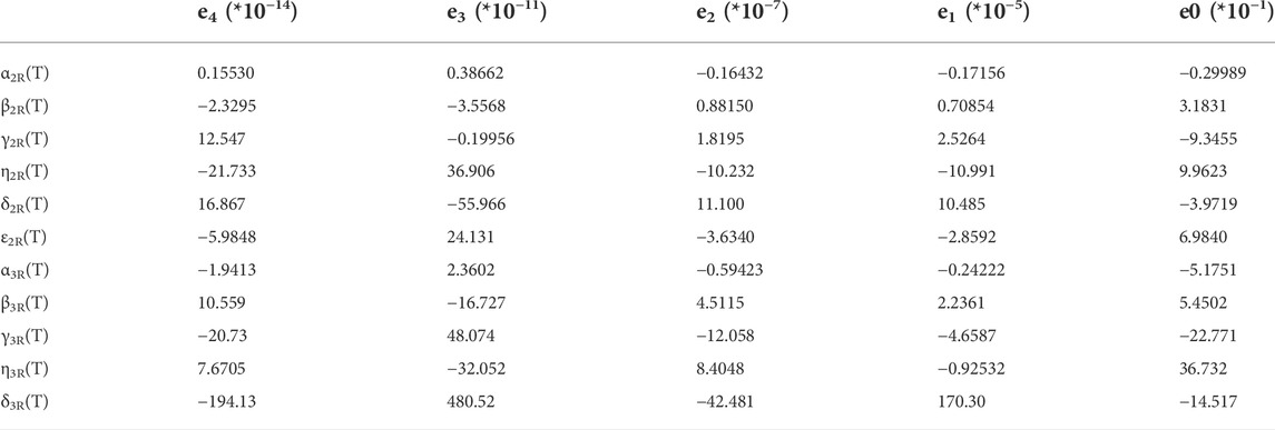
TABLE 8. Fitting parameters for
As mentioned previously, the Λ-graded structure is studied under fully strained to GaN and bulk relaxed conditions. In the absence of strain, pyro-electric polarization (spontaneous polarization) is the only polarization in the system:
which is defined for
In contrast, in the presence of strain, piezo-electric polarization would be added to charges due to polarization (Belghouthi et al., 2016).
The piezo-electric polarization of the base InN and GaN are given by
Then, the total polarization is given by the simple sum of the piezo and the spontaneous components. The induced charges due to pyroelectric polarization are shown in Figure 6A. In addition, electron concentrations in the structure are given for T = 100 K in Figure 5B. It is seen that a significant electron distribution penetrates into the p-type region for xmax > 60%. At a maximum, when xmax = 100%, the electron distribution is seen to penetrate ∼15 nm into the p-type region. When pyro-electric charges are negative, it means that the bound charges are negative, so holes are attracted making it a p-type region. On the other hand, positive, bound, pyro-electric charges make an n-type region. It can be seen in Figure 5A that the pyro-electric background charge changes type roughly halfway through the layer, becoming a significant contribution to xmax >∼60%. As a result, the simple p-n diode structure assumed for the device changes ultimately to a p-n--p--n-type structure.
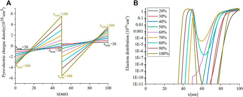
FIGURE 5. (A) Pyro-electric charge density distribution in different xmax and (B) electron charge distribution in different xmax for the relaxed case.
Figure 6A shows both the electron and hole concentration for the xmax = 100% case. Here, the p-n-p-n-type structure can be seen; however, the hole concentration between ∼60 and ∼80 nm has effectively compensated the free electrons leaving the material with vanishingly small free carriers of either type. However, now, we see for the band diagram of the xmax = 100% device in Figure 6B that there are additional barriers for the current to flow through the device. This results in increased Voc which we will see in the following paragraphs.
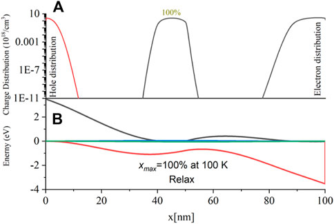
FIGURE 6. (A) Charge distribution for x = 100% and (B) energy band diagram for 100% under the relaxed condition (both at room temperature).
Now, with the absorption coefficients as functions of the band gap, which is a function of the temperature and composition, under strained and relaxed conditions, we can determine the generation rate as explained previously. This is shown for xmax = 70% in Figures 7A,B for the bulk relaxed case and the strained to GaN case, respectively, over the temperature ranging from 100 K to 800 K. It can be seen that the strained material reaches much higher generation rates due to the lower band gap. At the same time, it is evident that the generation rates generally increase as a result of increasing temperature. This is also due to the decreasing band gap as the temperature increases.
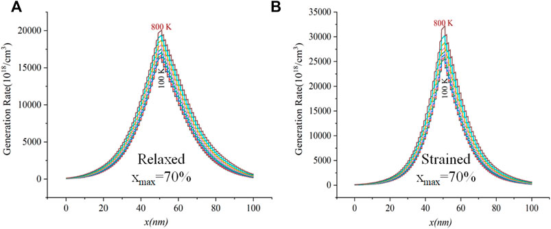
FIGURE 7. Generation rate for xmax = 70% in different temperatures. (A) Relaxed. (B) Strained.
By importing the generation rates into nextnano, the J-V curves used to calculate solar cell parameters can be calculated. Figures 8A,B show the J-V curves, again for xmax = 70%, for relaxed and strained materials, respectively, as the temperature is changed from 100 K to 800 K. Here, it can be seen that as the temperature decreases, the J-V curves become more like an ideal diode curve.
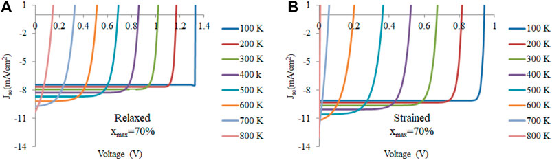
FIGURE 8. J-V curve for xmax = 70% for both the (A) relaxed condition and (B) strained condition are given at different temperatures (100–800 K).
Other solar cell parameters such as open-circuit voltage (Voc), short-circuit current density (Jsc), and solar efficiency for different xmax and T are obtained from the J-V curves. As seen in Figure 10B, for the strained devices, Voc decreases with an increase in xmax, that is, a decrease in the band gap, which was expected (Green, 1998; Green, 1981). Under relaxed condition, the Voc behavior is not linear with the band gap, as seen in Figure 10A. As shown previously in Figure 6, the electrons penetrate into the p-type region. At xmax > 80%, when the penetrated charge density is almost equal to polarization doping charge, Voc begins to increase. It means that for xmax > 80% at low temperatures, Voc is increased as energy band diagrams and shows the p-n-p-n structure instead of the p-n structure. However, the second p-layer is relatively weak. We believe that the changing carrier charge density for xmax > 80% is the main reason for the increasing Voc, as shown in Figure 7. Finally, Figure 9C shows more details for Voc at room temperature for high indium concentrations. Here, it can be seen that at xmax = ∼88%, Voc increases due to the charge penetration into the p-region and the resulting p-n-p-n structure. As shown in Figure 6B, Figure 7, doping concentrations due to structure change and carrier distribution are not linear.
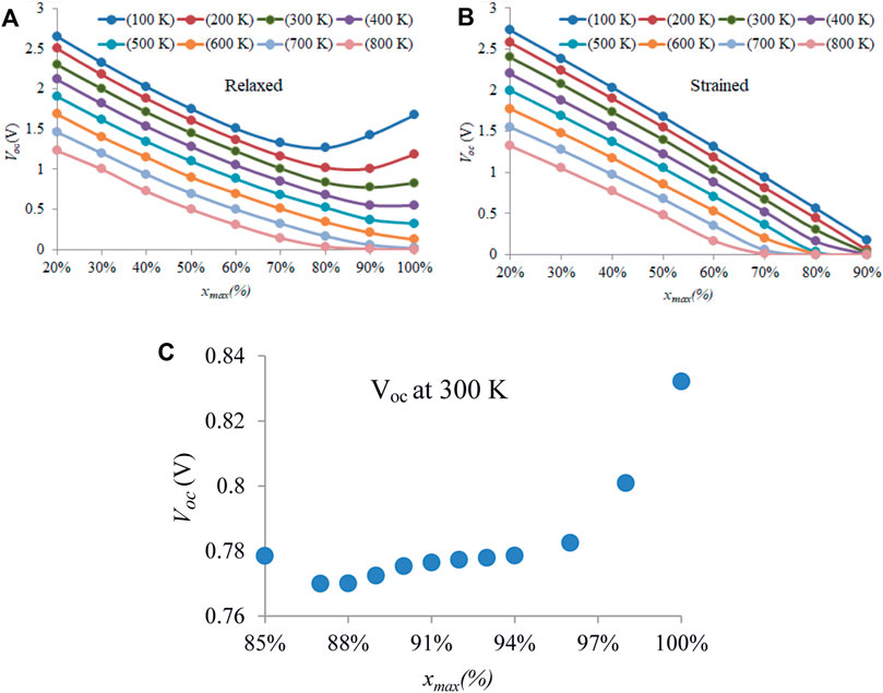
FIGURE 9. (A) and (B) Voc for both relaxed and strained conditions at different temperatures for different xmax (C) at room temperature for xmax = 85%–100%.
The open-circuit voltage, Voc, for the relaxed and strained conditions are shown in Figures 9A,B, respectively, while the short-circuit current density, Jsc, for the relaxed and strained conditions is shown in Figures 10A,B, respectively. Generally, Jsc increases when the indium composition increases and lowers the band gap (Green, 1998; Green, 1981).
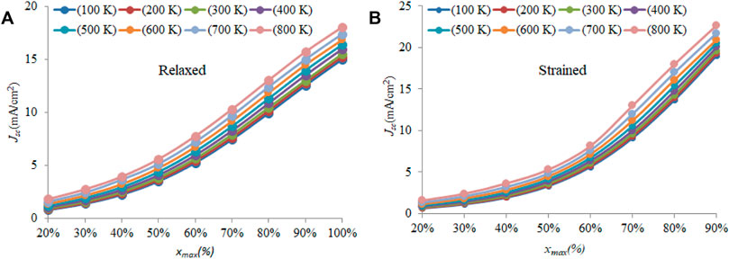
FIGURE 10. Jsc for both (A) relaxed and (B) strained conditions at different temperatures for different xmax.
The fill factors were calculated and are displayed in Figures 11A,B for both the relaxed and strained devices, respectively. Under both conditions, the FF generally decreases as xmax increases. Similarly, as expected, the FF decreases with an increasing temperature. For the relaxed case, this is a relatively stable linear decay, which increases as xmax increases. However, for the strained case, the FF rapidly vanishes at the highest xmax values.
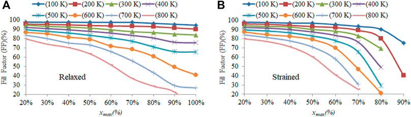
FIGURE 11. Fill factor for the (A) relaxed condition and (B) strained condition for different temperatures. The lines are just guides to the eye.
Finally, the total solar efficiency was calculated for all cases. This can be calculated using the following formula:
Figures 12A,Bshow the solar efficiencies as functions of xmax, for temperatures ranging from 100 K to 800 K, for the relaxed and strained devices, respectively. Under the relaxed condition, the devices reach the maximum efficiency when xmax = 100%, that is, InN, for the lower temperatures from 100 to 400 K. For the higher temperatures, the maximum efficiency shifts toward lower xmax.
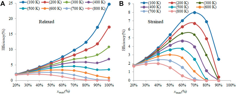
FIGURE 12. Efficiency for both (A) relaxed and (B) strained conditions at different temperatures for different xmax.
For the strained structures, the maximum efficiency from high to low temperatures is linearly shifted toward low xmax due to sharp dropping of Voc for high xmax at high temperatures which reduces Pmax.
Figure 13 summarizes xmax found to maximize the efficiency for each temperature for both the strained and relaxed cases. Here, we see that for the strained structure, the maximum xmax decreases monotonically from 71% to 37% as the temperature increases. At the same time, though, for the relaxed structures, for low temperatures (100–400 K), the maximum xmax is 100%, while for higher temperatures (500–800 K), it also demonstrates a monotonic decrease from ∼65% to 35%.
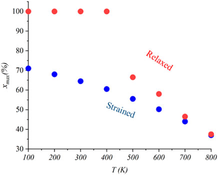
FIGURE 13. xmax for the maximum efficiency at different temperatures for relaxed and strained structures.
The maximum efficiencies found for each maximum xmax at each temperature is given in Figure 14. It shows that the efficiency for the relaxed structures at low temperatures is much higher than that for the strained structures, which are due to the sudden drop in Voc at low temperatures. The maximum efficiency at high temperatures monotonically decreases and is almost the same as the strained structure at high temperatures (600–800 K).
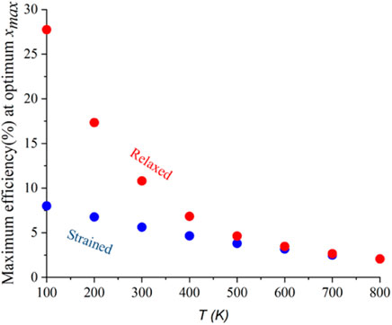
FIGURE 14. Maximum efficiency corresponded to optimum xmax for relaxed and strained structures.
Conclusion
Λ-graded InGaN solar cells were designed to make p-n junction solar cells by polarization doping. Solar cell parameters under both bulk relaxed conditions and fully strained to GaN conditions were studied using nextnano software. A Vegard’s law-like equation was defined to calculate the energy band gap under strained conditions as functions of temperature. Several fitting methods were performed to have analytical representations of the absorption coefficient as a function of band gap and temperature (for both relaxed and strained structures). In order to perform the simulations, the graded structures were converted to step-graded structures with a 1-nm step. The generation rate was obtained for each layer, then imported into nextnano software in order to simulate the light J-V curves. The solar cell parameters were then extracted from these structures under strained and relaxed conditions. Voc for the relaxed structures sharply increase for low temperatures (100–400 K). The free carrier densities and band structures for these structures show that the as-designed p-n diode structures are converted into p-n-p-n structures due to the conversion of the polarization charge density from negative to positive within the compositional grading as a result of the effective bowing parameter of the InGaN polarization. Finally, the maximum xmax was determined for each temperature for both strained and relaxed conditions. This work demonstrates that this Λ-graded InGaN solar cell design could be extremely useful in constructing a solar cell for the purpose of operating in high-temperature environments. At the same time, these designs have shown great potential overall with efficiencies up to ∼25% for thin-film designs of only 100 nm. Thicker films would most certainly increase on this number.
Data availability statement
The original contributions presented in the study are included in the article; further inquiries can be directed to the corresponding authors.
Author contributions
MS: idea, Matlab—nextnano simulation, literature review, and writing. MZ-A: MATLAB simulation. MA: nextnano simulation. RA: literature review and MATLAB simulation. MM: literature review—writing—solar cell. MR: literature review—material. RA: literature review—material. YM: supervision. MW: PI, main idea, supervision, and writing.
Conflict of interest
The authors declare that the research was conducted in the absence of any commercial or financial relationships that could be construed as a potential conflict of interest.
Publisher’s note
All claims expressed in this article are solely those of the authors and do not necessarily represent those of their affiliated organizations, or those of the publisher, the editors, and the reviewers. Any product that may be evaluated in this article, or claim that may be made by its manufacturer, is not guaranteed or endorsed by the publisher.
References
Adeeb, J., Farhan, A., and Al-Salaymeh, A. (2019). Temperature effect on performance of different solar cell Technologies. J. Ecol. Eng. 20 (5), 249–254. doi:10.12911/22998993/105543
Alam, S. N., Zubialevich, V. Z., Ghafary, B., and Parbrook, P. J. (2020). Bandgap and refractive index estimates of InAlN and related nitrides across their full composition ranges. Sci. Rep. 10 (1), 16205. doi:10.1038/s41598-020-73160-7
Azize, M., and Palacios, T. (2010). Effect of substrate-induced strain in the transport properties of AlGaN/GaN heterostructures. J. Appl. Phys. 108 (2), 023707. doi:10.1063/1.3463150
Belghouthi, R., and Aillerie, M. (2019). Temperature dependence of inGaN/GaN multiple quantum well solar cells. Energy Procedia 157, 793–801. doi:10.1016/j.egypro.2018.11.245
Belghouthi, R., Salvestrini, J. P., Gazzeh, M. H., and Chevallier, C. (2016). Analytical modeling of polarization effects in InGaN double hetero-junction p-i-n solar cells. Superlattices Microstruct. 100, 168–178. doi:10.1016/j.spmi.2016.09.016
Belghouthi, R., Taamalli, S., Echouchene, F., Mejri, H., and Belmabrouk, H. (2015). Modeling of polarization charge in N-face InGaN/GaN MQW solar cells. Mater. Sci. Semicond. Process. 40, 424–428. doi:10.1016/j.mssp.2015.07.009
Bhuiyan, A. G., Sugita, K., Hashimoto, A., and Yamamoto, A. (2012). InGaN solar cells: Present state of the Art and important challenges. IEEE J. Photovoltaics 2 (3), 276–293. doi:10.1109/JPHOTOV.2012.2193384
Birner, S., Hackenbuchner, S., Sabathil, M., Zandler, G., Majewski, J., Andlauer, T., et al. (2006). Modeling of semiconductor Nanostructures with nextnano 3. Acta Phys. Pol. A 110 (2), 111–124. doi:10.12693/APhysPolA.110.111
Blakesley, J. C., and Neher, D. (2011). Relationship between energetic disorder and open-circuit voltage in bulk heterojunction organic solar cells. Phys. Rev. B 84 (7), 075210. doi:10.1103/PhysRevB.84.075210
Boney, C., Pillai, R., Starikov, D., and Bensaoula, A. (2012). “Properties and modelling of InGaN for high temperature photovoltaics,” in 2012 38th IEEE Photovoltaic Specialists Conference, Austin, TX, USA, 03-08 June 2012 (IEEE), 002509–002512. doi:10.1109/PVSC.2012.6318104
Brochen, S., Brault, J., Chenot, S., Dussaigne, A., Leroux, M., and Damilano, B. (2013). Dependence of the Mg-related acceptor ionization energy with the acceptor concentration in p-type GaN layers grown by molecular beam epitaxy. Appl. Phys. Lett. 103 (3), 032102. doi:10.1063/1.4813598
Brown, G. F., Ager, J. W., Walukiewicz, W., and Wu, J. (2010). Finite element simulations of compositionally graded InGaN solar cells. Sol. Energy Mater. Sol. Cells 94 (3), 478–483. doi:10.1016/j.solmat.2009.11.010
Caro, M. A., Schulz, S., and O’Reilly, E. P. (2013). Theory of local electric polarization and its relation to internal strain: Impact on polarization potential and electronic properties of group-III nitrides. Phys. Rev. B 88 (21), 214103. doi:10.1103/PhysRevB.88.214103
Cheriton, R., Sadaf, S. M., Robichaud, L., Krich, J. J., Mi, Z., and Hinzer, K. (2020). Two-photon photocurrent in InGaN/GaN nanowire intermediate band solar cells. Commun. Mater 1 (1), 63. doi:10.1038/s43246-020-00054-6
Cho, Y., Yamaguchi, A., Uehara, R., Yasuhara, S., Hoshina, T., and Miyauchi, M. (2020). Temperature dependence on bandgap of semiconductor photocatalysts. J. Chem. Phys. 152 (23), 231101. doi:10.1063/5.0012330
David, A., and Grundmann, M. J. (2010). Influence of polarization fields on carrier lifetime and recombination rates in InGaN-based light-emitting diodes. Appl. Phys. Lett. 97 (3), 033501. doi:10.1063/1.3462916
Dreyer, C. E., Janotti, A., and Van de Walle, C. G. (2013). Effects of strain on the electron effective mass in GaN and AlN. Appl. Phys. Lett. 102 (14), 142105. doi:10.1063/1.4801520
Feng, S.-W., Lai, C.-M., Tsai, C.-Y., Su, Y.-R., and Tu, L.-W. (2013). Modeling of InGaN p-n junction solar cells. Opt. Mater. Express 3 (10), 1777, Oct. doi:10.1364/OME.3.001777
Giannoccaro, G., De Leonardis, F., and Passaro, V. (2016), 3. , 5. doi:10.3390/photonics3010005Modeling of the Interminiband Absorption coefficient in InGaN quantum Dot superlattices, Photonics
Golam Sarwar, A. T. M., and Myers, R. C. (2012). Exploiting piezoelectric charge for high performance graded InGaN nanowire solar cells. Appl. Phys. Lett. 101 (14), 143905. doi:10.1063/1.4757990
Green, M. A. (1981). Solar cell fill factors: General graph and empirical expressions. Solid-State Electron. 24 (8), 788–789. doi:10.1016/0038-1101(81)90062-9
Green, M. A. (1998). Solar cells: Operating principles, technology and system applications. Englewood Cliffs, NJKensington, NSW: Univ. of New South Wales.
Kazazis, S. A., Papadomanolaki, E., Androulidaki, M., Kayambaki, M., and Iliopoulos, E. (2018). Optical properties of InGaN thin films in the entire composition range. J. Appl. Phys. 123 (12), 125101. doi:10.1063/1.5020988
Kucukgok, B., Wu, X., Wang, X., Liu, Z., Ferguson, I. T., and Lu, N. (2016). The structural properties of InGaN alloys and the interdependence on the thermoelectric behavior. AIP Adv. 6 (2), 025305. doi:10.1063/1.4941934
Kuo, Y.-K., Lin, W.-W., and Lin, J. (2001). Band-gap bowing parameter of the in x Ga 1- x N derived from theoretical simulation. Jpn. J. Appl. Phys. 40, 3157–3158. doi:10.1143/JJAP.40.3157
Lee, Y.-J., Yao, Y.-C., and Yang, Z.-P. (2015). Numerical Analysis on polarization-induced doping III-nitride n-i-p solar cells. IEEE Photonics J. 7 (1), 1–9. doi:10.1109/JPHOT.2015.2392374
LeGoues, F. K., Meyerson, B. S., Morar, J. F., and Kirchner, P. D. (1992). Mechanism and conditions for anomalous strain relaxation in graded thin films and superlattices. J. Appl. Phys. 71 (9), 4230–4243. doi:10.1063/1.350803
Li, S., Ware, M., Wu, J., Minor, P., Wang, Z., Wu, Z., et al. (2012). Polarization induced pn-junction without dopant in graded AlGaN coherently strained on GaN. Appl. Phys. Lett. 101 (12), 122103. doi:10.1063/1.4753993
Lv, Z., Guo, Y., Zhang, S., Wen, Q., and Jiang, H. (2021). Polarization engineered InGaN/GaN visible-light photodiodes featuring high responsivity, bandpass response, and high speed. J. Mater. Chem. C 9 (36), 12273–12280. doi:10.1039/D1TC01193F
Masui, H., Yamada, H., Iso, K., Nakamura, S., and DenBaars, S. P. (2008). Optical polarization characteristics of m -oriented InGaN/GaN light-emitting diodes with various indium compositions in single-quantum-well structure. J. Phys. D. Appl. Phys. 41 (22), 225104. doi:10.1088/0022-3727/41/22/225104
Mesrane, A., Rahmoune, F., Mahrane, A., and Oulebsir, A. (2015). Design and simulation of InGaNp-nJunction solar cell. Int. J. Photoenergy 2015, 1–9. doi:10.1155/2015/594858
Moret, M., Gil, B., Ruffenach, S., Briot, O., Giesen, C., Heuken, M., et al. (2009). Optical, structural investigations and band-gap bowing parameter of GaInN alloys. J. Cryst. Growth 311 (10), 2795–2797. doi:10.1016/j.jcrysgro.2009.01.009
Moses, P. G., Miao, M., Yan, Q., and Van de Walle, C. G. (2011). Hybrid functional investigations of band gaps and band alignments for AlN, GaN, InN, and InGaN. J. Chem. Phys. 134 (8), 084703. doi:10.1063/1.3548872
Nakamura, S., Senoh, M., Iwasa, N., Nagahama, S., Yamada, T., and Mukai, T. (1995). Superbright green InGaN single-quantum-well-structure light-emitting diodes. Jpn. J. Appl. Phys. (2008). 34, L1332–L1335. doi:10.1143/JJAP.34.L1332
Nakamura, S., Senoh, M., Nagahama, S. i., Iwasa, N., Yamada, T., Matsushita, T., et al. (1996). InGaN-Based multi-quantum-well-structure Laser diodes. Jpn. J. Appl. Phys. (2008). 35, L74–L76. doi:10.1143/JJAP.35.L74
Narita, T., Yoshida, H., Tomita, K., Kataoka, K., Sakurai, H., Horita, M., et al. (2020). Progress on and challenges of p-type formation for GaN power devices. J. Appl. Phys. 128 (9), 090901. doi:10.1063/5.0022198
Nawaz, M., and Ahmad, A. (2012). A TCAD-based modeling of GaN/InGaN/Si solar cells. Semicond. Sci. Technol. 27 (3), 035019. doi:10.1088/0268-1242/27/3/035019
Nextnano, N. (2021). qcl:electronic_band_structure [nextnano.NEGF - software for Quantum Transport. AvaliableAt: https://nextnano-docu.northeurope.cloudapp.azure.com/dokuwiki/doku.php?id=qcl:electronic_band_structure.
Obloh, H., Bachem, K., Kaufmann, U., Kunzer, M., Maier, M., Ramakrishnan, A., et al. (1998). Self-compensation in Mg doped p-type GaN grown by MOCVD. J. Cryst. Growth 195 (1–4), 270–273. doi:10.1016/S0022-0248(98)00578-8
O’Donnell, K. P., and Chen, X. (1991). Temperature dependence of semiconductor band gaps. Appl. Phys. Lett. 58 (25), 2924–2926. doi:10.1063/1.104723
Park, S.-H., and Chuang, S.-L. (1999). Crystal-orientation effects on the piezoelectric field and electronic properties of strained wurtzite semiconductors. Phys. Rev. B 59 (7), 4725–4737. doi:10.1103/PhysRevB.59.4725
Pelá, R. R., Caetano, C., Marques, M., Ferreira, L. G., Furthmüller, J., and Teles, L. K. (2011). Accurate band gaps of AlGaN, InGaN, and AlInN alloys calculations based on LDA-1/2 approach. Appl. Phys. Lett. 98 (15), 151907. doi:10.1063/1.3576570
Pozina, G., Bergman, J. P., Monemar, B., Takeuchi, T., Amano, H., and Akasaki, I. (2000). Origin of multiple peak photoluminescence in InGaN/GaN multiple quantum wells. J. Appl. Phys. 88 (5), 2677–2681. doi:10.1063/1.1287124
Ra, Y.-H., and Lee, C.-R. (2019). Understanding the p-type GaN Nanocrystals on inGaN nanowire heterostructures. ACS Photonics 6 (10), 2397–2404. doi:10.1021/acsphotonics.9b01035
Romanov, A. E., Baker, T. J., Nakamura, S., and Speck, J. S., and (2006). Strain-induced polarization in wurtzite III-nitride semipolar layers. J. Appl. Phys. 100 (2), 023522. doi:10.1063/1.2218385
Routray, S. R., and Lenka, T. R. (2018). InGaN-based solar cells: A wide solar spectrum harvesting technology for twenty-first century. CSI Trans. ICT 6 (1), 83–96. doi:10.1007/s40012-017-0181-9
Sarollahi, M., Ghosh, P. K., Aldawsari, M. A., Davari, S., Refaei, M. I., Alhelais, R., et al. (2021). Experiment-simulation comparison of luminescence properties of GaN/InGaN/GaN double graded structures. J. Luminescence 240, 11841–12021. doi:10.1016/j.jlumin.2021.118411
Sarollahi, M., Ghosh, P. K., Aldawsari, M. A., Kuchuk, A., and Ware, M. E. (2020). Luminescence properties of GaN/InxGa1−xN/InyGa1−yN double graded structures (Zigzag quantum wells). J. Electron. Mater 49 (6), 3512–3519. doi:10.1007/s11664-020-08033-w
Sarollahi, M., Zamani Alavijeh, M., Aldawsari, M. A., Allaparthi, R., Alhelais, R., Refaei, M. A., et al. (2022). Modeling of Λ-graded InxGa1−xN solar cells: Comparison of strained and relaxed features. J. Phot. Energy 12 (02), 22205. doi:10.1117/1.JPE.12.022205
Shen, X., Lin, S., Li, F., Wei, Y., Zhong, S., Li, J., et al. (2008). “Simulation of the InGaN-based tandem solar cells,” in Proceedings Volume 7045, Photovoltaic Cell and Module Technologies II (San Diego, CA: SPIE).
Simon, J., Protasenko, V., Lian, C., Xing, H., and Jena, D. (2010). Polarization-induced hole doping in wide–band-gap Uniaxial semiconductor heterostructures. Science 327 (5961), 60–64. doi:10.1126/science.1183226
Van de Walle, C. G., and Segev, D. (2007). Microscopic origins of surface states on nitride surfaces. J. Appl. Phys. 101 (8), 081704. doi:10.1063/1.2722731
Vurgaftman, I., and Meyer, J. R. (2003). Band parameters for nitrogen-containing semiconductors. J. Appl. Phys. 94 (6), 3675–3696. doi:10.1063/1.1600519
Vurgaftman, I., Meyer, J. R., and Ram-Mohan, L. R. (2001). Band parameters for III–V compound semiconductors and their alloys. J. Appl. Phys. 89 (11), 5815–5875. doi:10.1063/1.1368156
Wierer, J. J., Fischer, A. J., and Koleske, D. D. (2010). The impact of piezoelectric polarization and nonradiative recombination on the performance of (0001) face GaN/InGaN photovoltaic devices. Appl. Phys. Lett. 96 (5), 051107. doi:10.1063/1.3301262
Wu, J., Walukiewicz, W., Shan, W., Yu, K. M., Ager, J. W., Li, S. X., et al. (2003). Temperature dependence of the fundamental band gap of InN. J. Appl. Phys. 94 (7), 4457–4460. doi:10.1063/1.1605815
Wu, J., Walukiewicz, W., Yu, K. M., Ager, J. W., Haller, E. E., Lu, H., et al. (2002). Small band gap bowing in In1−xGaxN alloys. Appl. Phys. Lett. 80 (25), 4741–4743. doi:10.1063/1.1489481
Zhang, X., Wang, X., Xiao, H., Yang, C., Ran, J., Wang, C., et al. (2007). Simulation of in 0.65 Ga 0.35 N single-junction solar cell. J. Phys. D. Appl. Phys. 40 (23), 7335–7338. doi:10.1088/0022-3727/40/23/013
Keywords: solar cell, InGaN alloy, polarization doping, graded structure, strain, relax
Citation: Sarollahi M, Zamani-Alavijeh M, Aldawsari MA, Allaparthi R, Maruf MHU, Refaei M, Alhelais R, Mazur YI and Ware ME (2022) Modeling of temperature dependence of Λ-graded InGaN solar cells for both strained and relaxed features. Front. Mater. 9:1006071. doi: 10.3389/fmats.2022.1006071
Received: 28 July 2022; Accepted: 05 October 2022;
Published: 28 October 2022.
Edited by:
Yi Gu, Shanghai Institute of Technical Physics (CAS), ChinaReviewed by:
Soumyaranjan Routray, SRM Institute of Science and Technology, IndiaTao Wang, Peking University, China
Copyright © 2022 Sarollahi, Zamani-Alavijeh, Aldawsari, Allaparthi, Maruf, Refaei, Alhelais, Mazur and Ware. This is an open-access article distributed under the terms of the Creative Commons Attribution License (CC BY). The use, distribution or reproduction in other forums is permitted, provided the original author(s) and the copyright owner(s) are credited and that the original publication in this journal is cited, in accordance with accepted academic practice. No use, distribution or reproduction is permitted which does not comply with these terms.
*Correspondence: Morgan E. Ware, meware@uark.edu