Resistivity of Surface Steps in Bulk-Insulating Topological Insulators
 Wonhee Ko
 Saban Hus
 Hoil Kim2,3
  An-Ping Li
- 1Center for Nanophase Materials Sciences, Oak Ridge National Laboratory, Oak Ridge, TN, United States
- 2Department of Physics, Pohang University of Science and Technology, Pohang, Korea
- 3Center for Artificial Low Dimensional Electronic Systems, Institute for Basic Science, Pohang, Korea
- 4Department of Physics and Quantum Theory Project, University of Florida, Gainesville, FL, United States
Electron transport in topological insulators usually involves both topologically protected surface states and trivial electronic states in the bulk material. The surface transport is particularly interesting; however, it is also susceptible to atomic defects on the surfaces, such as vacancies, impurities, and step edges. Experimental determination of scattering effects of these surface defects requires both nanoscale spatial resolution and the ability to decipher surface transport from bulk transport. Here we directly measure the resistivity of individual surface steps in the surface dominating transport process of topological insulator Bi2Te2Se. A variable probe-spacing transport spectroscopy with a multiprobe scanning tunneling microscope is used to differentiate the surface conductance from bulk conductance, allowing the identification of a surface dominant transport regime. The technique also reveals a deviation from ideal 2D transport at atomic steps. Then, a multi-probe scanning tunneling potentiometry is employed to visualize the electrochemical potentials across individual step edges. A quantitative analysis of the potential distributions enables us to acquire a resistivity of 0.530 mΩ · cm for the one quintuple-layer atomic step. The result indicates that atomic defects, despite preserving the time-reversal symmetry, can still significantly affect the transport in topological insulators.
Introduction
Charge transport in topological insulators is distinct from the transport in trivial materials due to the topological surface states. Although the bulk is insulating, the metallic surface states are created by the non-trivial topology of the bulk band and guaranteed to exist regardless of the surface geometry (Hasan and Kane, 2010; Qi and Zhang, 2011). The topological surface states further differ from trivial states as the electrons occupying them behave like massless Dirac fermions and possess a unique spin texture from spin-momentum locking. Because deflection of charge carrier momentum by defects should be accompanied by the rotation of spin, backscattering is strictly prohibited when the defects preserve the time-reversal symmetry. Hence, it is predicted that the scattering of charge carriers by defects on the surface of topological insulators are disparate from other 2D electron systems, and intensive theoretical and experimental studies were prompted on intrinsic, time-reversal-symmetry preserving defects such as vacancies, antisites, and step edges (Alpichshev et al., 2010; Biswas and Balatsky, 2010; Alpichshev et al., 2012; Black-Schaffer and Balatsky, 2012).
Scanning tunneling microscopy (STM) can resolve atomic and electronic structures in atomic resolution, so it is widely used to study the atomic steps and defects on the surface of topological insulators (Yin et al., 2021; Lüpke et al., 2022). However, understanding and quantifying the role of defects on transport through topological surface states by STM are still challenging for two main reasons with respect to materials and STM measurement techniques. First, most of the topological insulators have substantial bulk carriers due to the relatively small bulk band gap and unintentional doping from intrinsic defects that significantly hamper the transport through the surface (Ando, 2013). One way to cope with this problem is to reduce the sample thickness down to a few tens of nanometers so the ratio of bulk to surface carriers becomes minimal (Koirala et al., 2015; Bauer and Bobisch, 2016; 2017; Lüpke et al., 2017). However, transport in thin-film topological insulators incorporates the multiple surface states at the top and bottom of the surface which makes the current distribution more complicated between these two surfaces (Lüpke et al., 2018; Just et al., 2020). Furthermore, when films are too thin, the top and bottom surface states can couple and change their topology (Zhang et al., 2010). Secondly, understanding charge transport across the atomic defects requires a in situ and operando atomic-scale mapping of topography and surface potential during the current flow. For the traditional single-probe STM, flowing current to the sample requires additional electrodes deposited by lithography which significantly contaminates the surface of topological insulators to deteriorate the surface transport properties (Checkelsky et al., 2011).
In this paper, we used multi-probe STM and observed single crystal of bulk-insulating topological insulators to overcome these challenges (Kim et al., 2007; Hus et al., 2017). It has been known that Bi and Sb chalcogenides are topological insulators whose Fermi level can be adjusted by changing the ratio between the elements (Ren et al., 2011; Arakane et al., 2012). Among various compositions, we chose Bi2Te2Se for our measurement since its bulk-insulating properties are well-known by ex situ transport measurement (Ren et al., 2010). Then, two spectroscopic techniques of multi-probe STM were employed to confirm the surface dominant transport and scattering of surface charge carriers by atomic steps whose smallest unit is a quintuple layer (QL) composed of Te-Bi-Te-Bi-Te sub-layers. The variable probe-spacing transport spectroscopy (VPTS) was utilized to confirm the surface dominant transport at low temperature of 82 K and small source probe distance below 10 μm (Ko et al., 2018). Moreover, deviation from the ideal surface transport by atomic steps was observed by VPTS on stepped surface. More quantitative measurements of the effect of atomic steps on the surface transport have been achieved by scanning tunneling potentiometry (STP) (Clark et al., 2013; Li et al., 2013). STP enabled us to precisely map the surface potential during a current flow and measure the voltage drop across atomic steps that results in the quantitative determination of the step resistivity. The result shows that atomic defects, despite preserving the time-reversal symmetry, can still significantly affects the transport through topological surface states.
Materials and Methods
Sample Preparation
Single crystal of Bi2Te2Se was grown by the self-flux method following the previously reported procedure (Ren et al., 2010). Bulk-insulating property of the Bi2Te2Se was confirmed by ex situ transport measurement with physical property measurements system (PPMS), which displayed increasing bulk resistivity with decreasing temperature (Ko et al., 2018). In situ transport and STP measurements were done at the cryogenic four-probe STM, operating at ultrahigh vacuum (< 8 × 10⁻¹⁰ Torr) and temperature of 82 K (Kim et al., 2007). The samples were cleaved inside the ultrahigh-vacuum chamber and then transferred to the STM stage without any exposure to the ambient environment. Etched tungsten tips were used as STM probes, whose metallic behavior was checked on gold foil before each measurement. The samples are confirmed to be thicker than 500 μm after cleaving which ensures no crosstalk between the top and bottom surface states or leakage current to the sample holder.
Variable Probe-Spacing Transport Spectroscopy
VPTS spectroscopy was acquired by performing four-probe transport measurements in collinear configuration while changing the position of two inner voltage probes (Durand et al., 2016; Hus et al., 2017; Ko et al., 2018). Figure 1A illustrates the measurement scheme over the surface with atomic steps. Here, two outer probes supply the source current while two inner probes measure the potential difference. The potential drop between the inner probes is measured for a large set of inter-probe distances measured by scanning electron microscope (SEM). In topological insulators, transport occurs through two conduction channels of the topological surface states and the trivial bulk states. Assuming uniform and isotropic 2D and 3D resistivity for surface and bulk, respectively, the four-probe resistance can be expressed as a function of probe spacings (Durand et al., 2016) as
where ΔV is the potential drop between the inner voltage probes, Is is the source current applied through the outer current probes, ρ2D is the surface resistivity, sij is the distance between the probes i and j, and g = (ρ2D/ρ3D)s14 is a dimensionless parameter which gives the ratio of the surface and bulk resistivity. The model indicates that R vs. Xg should be linear when the correct value of g is substituted.
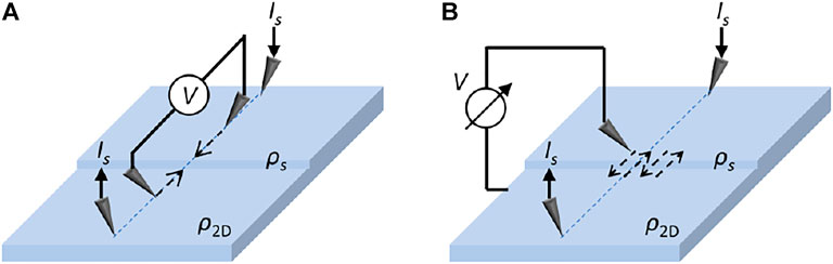
FIGURE 1. Measurement scheme of (A) variable probe-spacing transport spectroscopy and (B) scanning tunneling potentiometry, which are utilized for studying transport across the atomic steps on the surface of topological insulators.
Scanning Tunneling Potentiometry
STP is a unique technique that combines transport with the scanning capability of STM (Clark et al., 2013; Li et al., 2013; Clark et al., 2014). The measurement schematic of STP is shown in Figure 1B. Here, two outer probes supply the source current while an inner probe scans the surface. To measure the potentiometry, we adopted the modified version of Feenstra and co-worker’s approach (Feenstra et al., 1986; Fein et al., 1987; Lüpke et al., 2015), where the scanning probe first moved to the new point and measured the surface topography at finite DC bias voltage by traditional STM feedback based on tunneling current, and then the STM feedback was turned off and a second feedback loop on the tip bias was turned on to track the surface potential by regulating tunneling current to zero. The resulting height and potential profile visualize the topography and potential of the scanned region.
Results
Variable Probe-Spacing Transport Spectroscopy on Bi2Te2Se Surface With Atomic Steps
VPTS was applied to Bi2Te2Se to observe the effect of atomic steps on the transport through the topological surface states. To exclude the effect of bulk conduction, the surface dominant transport was achieved by lowering the measurement temperature to 82 K and reducing the source probe distance below 10 μm (Ko et al., 2018). Figure 2A shows the SEM image of the surface of Bi2Te2Se that does not display any distinguishable steps, and Figure 2C shows the results of VPTS taken on this pristine surface with source probe distance s14 = 5.1 μm. The best linear fitting between R and Xg was achieved when g = 0, indicating that 100% of the electrical current is carried by the surface states. The linear fit results in the zero offset at Xg = 0 and the coefficient of determination r2 = 0.9981, showing that the measured four-probe resistances follow the theoretical prediction of homogenous surface resistivity. From the slope, surface resistivity is estimated to be ρ2D = 1835 ± 72 Ω. On the other hand, when there are two or more atomic steps between the probes (Figure 2B), measured resistance values become visibly deviated from the homogenous surface resistivity model (Figure 2D, also see Supplementary Figure S1), indicated by lower r2 = 0.9843 and nonzero offset at Xg = 0. Nevertheless, the best linear fit of R vs. Xg was achieved when g = 0 and the surface resistivity is estimated to be ρ2D = 2,211 ± 250 Ω, which is similar to the pristine surface. The value of fitting parameters indicates that the conduction is still dominated by the surface channel. The visible distortion of resistance values further supports the surface dominant transport, because the bulk conduction would not be affected by atomic steps due to their negligible thickness compared to the sample size (>500 μm). The results clearly show that the atomic steps disturb the transport of charge carriers through the topological surface states, even though the steps do not break time-reversal symmetry.
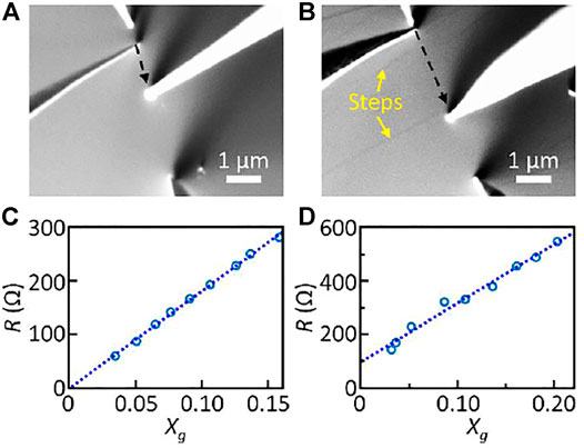
FIGURE 2. (A,B) SEM images of Bi2Te2Se surface without and with atomic steps, respectively. Four tips are placed in collinear configuration for variable probe-spacing transport spectroscopy. (C,D) Four-probe resistance R versus Xg of the surface without and with atomic steps, respectively.
Scanning Tunneling Potentiometry on Bi2Te2Se Surface With Atomic Steps
Further quantitative measurement is achieved by measuring the potential profile with STP across the single atomic step. Figure 3A shows the SEM image of a step edge and the probes placed for STP measurement. The distance between the outer probes was set to 7.9 μm to guarantee the surface dominant transport as confirmed by VPTS. Even though the SEM image can only resolve a single step, STM topography shows that there are two adjacent steps with the height of four QL and one QL (Figures 3B,E), where one QL corresponds to the height of ∼1 nm (Ren et al., 2010). Figure 3C shows the potential map obtained around these steps while flowing the current of 100 μA between the outer probes. Along the flat surface, a smooth potential gradient along the current direction (white arrow) is evident together with the sharp potential drops at the step edges. The potential drops at the step edges become clearer when the background slope is subtracted from the potential profile (Figure 3D). To confirm that these sharp potential drops are not artifacts, we measured the potential profiles across the step edge for various source-drain current values (Figure 3F). The profiles show that as the current increases both the overall slope of the potential and the magnitude of sharp drops at the step edges increase. The increase of potential drops at step edges becomes more visible after subtraction of the background slope (Figure 3G). The consistency between the STP map and single scan lines was confirmed by comparing voltage profiles from the line average of the map and the single scan line at the same current (Supplementary Figure S2).
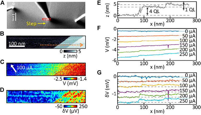
FIGURE 3. (A) SEM image of the surface with steps and three probes in STP configuration. The red box denotes the area where STP measurements were taken. (B) Topographic image of the area, (C) Raw STP map, and (D) STP map with the overall slope subtraction and low pass filtering for enhanced contrast across the steps. Line profile data of (E) height, (F) potential, and (G) potential with the slope subtracted plotted, which are taken along the orange dotted line in (B).
The resistivity of the surface and atomic steps can be extracted from the current dependence of the overall potential slope and potential drops at the steps, respectively. Since the scanned area is located close to the midpoint between the source probes and the scanning size of 500 nm is much smaller than the source probe distance of 7.9 μm, we can assume a constant current density
where
where 55° is the angle between the current and scan directions. The value of ρ2D is smaller than the one from VPTS, probably due to the aging of the surface that was exposed to a residual gas pressure of 2 × 10⁻⁹ torr for 4 days (Durand et al., 2016; Ko et al., 2018).
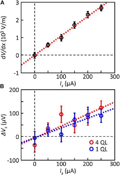
FIGURE 4. (A) Current dependence of the potential slope extracted from the line profiles in Figure 3F (B) Current dependence of the potential change across the step edges extracted from the line profiles in Figure 3G.
Figure 4B shows the measured potential drops at the step edges for different source currents. The voltage drops between the adjacent terraces were extracted by taking the average and standard deviation of the voltages inside the single terraces and then subtracted them to get the magnitude and error of the voltage drops (Supplementary Figure S3). Although the linear trend is less obvious due to the small signal-to-noise ratio, the general trend clearly shows an increasing magnitude of potential drop with the current. Linear fits result in the slope of ∆Vs/Is = 0.421 Ω for one QL step and ∆Vs/Is = 0.512 Ω for four QL step, which results in the step resistivity of ρs = ∆Vs/j = 0.530 mΩ · cm for one QL step and ρs = 0.646 mΩ · cm for four QL step. These results show that atomic steps as small as one QL can scatter charge carriers flowing through the topological surface states and behave as a potential barrier. The value of ρs is comparable to the previously reported value of ∼ 1 mΩ · cm for the steps on Bi chalcogenide thin films measured by STP (Bauer and Bobisch, 2016; 2017; Lüpke et al., 2017). Also, it is notable that the value of ρs is almost identical for one QL and four QL steps, which indicates that step resistivity is almost independent of the step height. Weak dependence of the resistivity on step height is in contrast with other trivial 2D metallic systems (Homoth et al., 2009; Ji et al., 2012; Clark et al., 2013; Clark et al., 2014) and might be related to the topological nature of the surface states. Revealing the origin of such behavior would require further systematic measurement of resistivity over various step heights and detailed theoretical modeling of atomic steps in topological insulators.
Discussion
We utilized multiprobe STM to perform VPTS and STP on the surface of Bi2Te2Se and measured how surface steps affect the transport of charge carriers through the topological surface states. Because the sample is bulk-insulating topological insulators, surface dominant transport was achieved and confirmed by VPTS at low temperature of 82 K and a source probe distance of less than 10 μm. On the stepped surface, in contrast, VPTS exhibited deviation from the ideal homogeneous 2D resistivity, manifested as outlying data points and offset at Xg = 0. STP was used for more quantitative measurement, which displayed potential slope across the flat surface and then sudden drop at the step edges. The step resistivity was estimated as ρs = 0.530 mΩ · cm for one QL step and ρs = 0.646 mΩ · cm for four QL step. Such nearly identical values of step resistivity for different heights are distinct from other trivial materials, which might be related to the topological nature of the surface transport. Our results indicate defects that do not break time-reversal symmetry can still affect the transport through topological surface states. Further STP studies on the effect of defect size and shape, and local magnetic states that can break time-reversal symmetry, will provide deeper insight on the transport through the topological insulators that can provide a crucial foundation for realizing topological quantum devices (He et al., 2022).
Data Availability Statement
The original contributions presented in the study are included in the article/Supplementary Material, further inquiries can be directed to the corresponding author.
Author Contributions
WK and A-PL designed the experiment. WK and SH performed multiprobe STM measurement. HK and JK grew the single crystal samples. X-GZ provided theoretical framework to analyze data. All authors contributed to writing the manuscript.
Funding
This work was supported by Center for Nanophase Materials Sciences (CNMS), which is a US Department of Energy, Office of Science User Facility at Oak Ridge National Laboratory. The sample preparation at POSTECH was supported by the Institute for Basic Science (IBS) through the Center for Artificial Low Dimensional Electronic Systems (no. IBS-R014-D1). The potentiometry data analysis by X-GZ was supported by the Center for Molecular Magnetic Quantum Materials, an Energy Frontier Research Center funded by the U.S. Department of Energy, Office of Science, Basic Energy Sciences under Award No. DE-SC0019330.
Conflict of Interest
The authors declare that the research was conducted in the absence of any commercial or financial relationships that could be construed as a potential conflict of interest.
Publisher’s Note
All claims expressed in this article are solely those of the authors and do not necessarily represent those of their affiliated organizations, or those of the publisher, the editors and the reviewers. Any product that may be evaluated in this article, or claim that may be made by its manufacturer, is not guaranteed or endorsed by the publisher.
Supplementary Material
The Supplementary Material for this article can be found online at: https://www.frontiersin.org/articles/10.3389/fmats.2022.887484/full#supplementary-material
References
Alpichshev, Z., Analytis, J. G., Chu, J. H., Fisher, I. R., Chen, Y. L., Shen, Z. X., et al. (2010). STM Imaging of Electronic Waves on the Surface of Bi2Te3: Topologically Protected Surface States and Hexagonal Warping Effects. Phys. Rev. Lett. 104 (1), 016401. doi:10.1103/PhysRevLett.104.016401
Alpichshev, Z., Biswas, R. R., Balatsky, A. V., Analytis, J. G., Chu, J.-H., Fisher, I. R., et al. (2012). STM Imaging of Impurity Resonances onBi2Se3. Phys. Rev. Lett. 108 (20), 206402. doi:10.1103/physrevlett.108.206402
Ando, Y. (2013). Topological Insulator Materials. J. Phys. Soc. Jpn. 82 (10), 102001. doi:10.7566/jpsj.82.102001
Arakane, T., Sato, T., Souma, S., Kosaka, K., Nakayama, K., Komatsu, M., et al. (2012). Tunable Dirac Cone in the Topological Insulator Bi2-xSbxTe3-ySey. Nat. Commun. 3, 636. doi:10.1038/ncomms1639
Bauer, S., and Bobisch, C. A. (2017). Electron Transport in Stepped Bi2Se3 Thin Films. J. Phys. Condens. Matter 29 (33), 334002. doi:10.1088/1361-648x/aa7a3c
Bauer, S., and Bobisch, C. A. (2016). Nanoscale Electron Transport at the Surface of a Topological Insulator. Nat. Commun. 7, 11381. doi:10.1038/ncomms11381
Biswas, R. R., and Balatsky, A. V. (2010). Impurity-induced States on the Surface of Three-Dimensional Topological Insulators. Phys. Rev. B 81 (23), 233405. doi:10.1103/physrevb.81.233405
Black-Schaffer, A. M., and Balatsky, A. V. (2012). Subsurface Impurities and Vacancies in a Three-Dimensional Topological Insulator. Phys. Rev. B 86 (11), 115433. doi:10.1103/physrevb.86.115433
Checkelsky, J. G., Hor, Y. S., Cava, R. J., and Ong, N. P. (2011). Bulk Band Gap and Surface State Conduction Observed in Voltage-Tuned Crystals of the Topological InsulatorBi2Se3. Phys. Rev. Lett. 106 (19), 196801. doi:10.1103/physrevlett.106.196801
Clark, K. W., Zhang, X. G., Gu, G., Park, J., He, G., Feenstra, R. M., et al. (2014). Energy gap Induced by Friedel Oscillations Manifested as Transport Asymmetry at Monolayer-Bilayer Graphene Boundaries. Phys. Rev. X 4 (1), 011021. doi:10.1103/physrevx.4.011021
Clark, K. W., Zhang, X.-G., Vlassiouk, I. V., He, G., Feenstra, R. M., and Li, A.-P. (2013). Spatially Resolved Mapping of Electrical Conductivity across Individual Domain (Grain) Boundaries in Graphene. ACS Nano 7 (9), 7956–7966. doi:10.1021/nn403056k
Durand, C., Zhang, X.-G., Hus, S. M., Ma, C., McGuire, M. A., Xu, Y., et al. (2016). Differentiation of Surface and Bulk Conductivities in Topological Insulators via Four-Probe Spectroscopy. Nano Lett. 16 (4), 2213–2220. doi:10.1021/acs.nanolett.5b04425
Feenstra, R. M., Thompson, W. A., and Fein, A. P. (1986). Real-space Observation Ofπ-Bonded Chains and Surface Disorder on Si(111)2×1. Phys. Rev. Lett. 56 (6), 608–611. doi:10.1103/physrevlett.56.608
Fein, A. P., Kirtley, J. R., and Feenstra, R. M. (1987). Scanning Tunneling Microscope for Low Temperature, High Magnetic Field, and Spatially Resolved Spectroscopy. Rev. Scientific Instr. 58 (10), 1806–1810. doi:10.1063/1.1139524
Hasan, M. Z., and Kane, C. L. (2010). Colloquium: Topological Insulators. Rev. Mod. Phys. 82 (4), 3045–3067. doi:10.1103/revmodphys.82.3045
He, Q. L., Hughes, T. L., Armitage, N. P., Tokura, Y., and Wang, K. L. (2022). Topological Spintronics and Magnetoelectronics. Nat. Mater. 21 (1), 15–23. doi:10.1038/s41563-021-01138-5
Homoth, J., Wenderoth, M., Druga, T., Winking, L., Ulbrich, R. G., Bobisch, C. A., et al. (2009). Electronic Transport on the Nanoscale: Ballistic Transmission and Ohm's Law. Nano Lett. 9 (4), 1588–1592. doi:10.1021/nl803783g
Hus, S. M., Zhang, X.-G., Nguyen, G. D., Ko, W., Baddorf, A. P., Chen, Y. P., et al. (2017). Detection of the Spin-Chemical Potential in Topological Insulators Using Spin-Polarized Four-Probe STM. Phys. Rev. Lett. 119 (13), 137202. doi:10.1103/physrevlett.119.137202
Ji, S.-H., Hannon, J. B., Tromp, R. M., Perebeinos, V., Tersoff, J., and Ross, F. M. (2012). Atomic-scale Transport in Epitaxial Graphene. Nat. Mater 11 (2), 114–119. doi:10.1038/nmat3170
Just, S., Lüpke, F., Cherepanov, V., Tautz, F. S., and Voigtländer, B. (2020). Parasitic Conduction Channels in Topological Insulator Thin Films. Phys. Rev. B 101 (24), 245413. doi:10.1103/physrevb.101.245413
Kim, T.-H., Wang, Z., Wendelken, J. F., Weitering, H. H., Li, W., and Li, A.-P. (2007). A Cryogenic Quadraprobe Scanning Tunneling Microscope System with Fabrication Capability for Nanotransport Research. Rev. Scientific Instr. 78 (12), 123701. doi:10.1063/1.2821610
Ko, W., Nguyen, G. D., Kim, H., Kim, J. S., Zhang, X.-G., and Li, A.-P. (2018). Accessing the Intrinsic Spin Transport in a Topological Insulator by Controlling the Crossover of Bulk-To-Surface Conductance. Phys. Rev. Lett. 121 (17), 176801. doi:10.1103/physrevlett.121.176801
Koirala, N., Brahlek, M., Salehi, M., Wu, L., Dai, J., Waugh, J., et al. (2015). Record Surface State Mobility and Quantum Hall Effect in Topological Insulator Thin Films via Interface Engineering. Nano Lett. 15 (12), 8245–8249. doi:10.1021/acs.nanolett.5b03770
Li, A.-P., Clark, K. W., Zhang, X.-G., and Baddorf, A. P. (2013). Electron Transport at the Nanometer-Scale Spatially Revealed by Four-Probe Scanning Tunneling Microscopy. Adv. Funct. Mater. 23 (20), 2509–2524. doi:10.1002/adfm.201203423
Lüpke, F., Eschbach, M., Heider, T., Lanius, M., Schüffelgen, P., Rosenbach, D., et al. (2017). Electrical Resistance of Individual Defects at a Topological Insulator Surface. Nat. Commun. 8, 15704. doi:10.1038/ncomms15704
Lüpke, F., Just, S., Eschbach, M., Heider, T., Młyńczak, E., Lanius, M., et al. (2018). In Situ disentangling Surface State Transport Channels of a Topological Insulator Thin Film by Gating. Npj Quan. Mater 3 (1), 46. doi:10.1038/s41535-018-0116-1
Lüpke, F., Korte, S., Cherepanov, V., and Voigtländer, B. (2015). Scanning Tunneling Potentiometry Implemented into a Multi-Tip Setup by Software. Rev. Sci. Instrum. 86 (12), 123701. doi:10.1063/1.4936079
Lüpke, F., Pham, A. D., Zhao, Y.-F., Zhou, L.-J., Lu, W., Briggs, E., et al. (2022). Local Manifestations of Thickness Dependent Topology and Axion Edge State in Topological Magnet MnBi2Te4. Phys. Rev. B 105 (3), 035423. doi:10.1103/PhysRevB.105.035423
Qi, X.-L., and Zhang, S.-C. (2011). Topological Insulators and Superconductors. Rev. Mod. Phys. 83 (4), 1057–1110. doi:10.1103/revmodphys.83.1057
Ren, Z., Taskin, A. A., Sasaki, S., Segawa, K., and Ando, Y. (2010). Large Bulk Resistivity and Surface Quantum Oscillations in the Topological insulatorBi2Te2Se. Phys. Rev. B 82 (24), 241306. doi:10.1103/physrevb.82.241306
Ren, Z., Taskin, A. A., Sasaki, S., Segawa, K., and Ando, Y. (2011). OptimizingBi2−xSbxTe3−ySeysolid Solutions to Approach the Intrinsic Topological Insulator Regime. Phys. Rev. B 84 (16), 165311. doi:10.1103/physrevb.84.165311
Yin, J.-X., Pan, S. H., and Zahid Hasan, M. (2021). Probing Topological Quantum Matter with Scanning Tunnelling Microscopy. Nat. Rev. Phys. 3 (4), 249–263. doi:10.1038/s42254-021-00293-7
Keywords: topological phase of matter, four-probe transport spectroscopy, atomic step, defect, topological insulator, electrical transport, topological surface states, scanning tunneling microscopy
Citation: Ko W, Hus S, Kim H, Kim JS, Zhang X-G and Li A-P (2022) Resistivity of Surface Steps in Bulk-Insulating Topological Insulators. Front. Mater. 9:887484. doi: 10.3389/fmats.2022.887484
Received: 01 March 2022; Accepted: 04 April 2022;
Published: 19 May 2022.
Edited by:
Cheng-Rong Hsing, Academia Sinica, TaiwanReviewed by:
Fanming Qu, Institute of Physics (CAS), ChinaMichael Dreyer, University of Maryland, College Park, United States
Copyright © 2022 Ko, Hus, Kim, Kim, Zhang and Li. This is an open-access article distributed under the terms of the Creative Commons Attribution License (CC BY). The use, distribution or reproduction in other forums is permitted, provided the original author(s) and the copyright owner(s) are credited and that the original publication in this journal is cited, in accordance with accepted academic practice. No use, distribution or reproduction is permitted which does not comply with these terms.
*Correspondence: An-Ping Li, apli@ornl.gov