Effect of strain profiling on anisotropic opto-electronic properties of As2X3 (X =S, Te) monolayers from first principles
 Eesha Andharia
 Hind Alqurashi3
  Bothina Hamad
 M. O. Manasreh
- 1Department of Physics, University of Arkansas, Fayetteville, AR, United States
- 2Materials Science and Engineering (MSEN), University of Arkansas, Fayetteville, AR, United States
- 3Physics Department, College of Science, Al-Baha University, Alaqiq, Saudi Arabia
- 4Department of Physics, Isra University, Amman, Jordan
- 5Physics Department, The University of Jordan, Amman, Jordan
- 6Department of Electrical Engineering, University of Arkansas, Fayetteville, AR, United States
Strain Engineering is a widely adopted approach to modulate the opto-electronic performance of 2-Dimensional (2D) materials. Recently, anisotropic Van der Waals (vdW) based 2D As2S3 monolayer has gained significant attention within the scientific community due to its stability in ambient conditions. Similar compounds like As2Te3 have also been theoretically explored. However, its indirect bandgap nature limits its application in optical devices. In this study, a systematic study of compressive and tensile strain on three profiles–Uniaxial along a-axis, Uniaxial along b-axis and biaxial strain from −10% to +10%, is performed for As2S3 and As2Te3 monolayers. Certain strain profiles like Uniaxial tensile strain of 8% along b-axis results in transition to direct bandgap material. Similarly, for As2Te3, shear strain of (−10%, +8%) along (a, b) axis results in direct bandgap material. In addition, the anisotropic optical absorption spectrum is obtained for unstrained and strained monolayers within the random phase approximation (RPA).
1 Introduction
Intrinsic in-plane structural anisotropy in vdW-based 2D materials gives rise to directionally dependent electronic, optical, magnetic, and mechanical properties that can be exploited for device physics. This class of materials known as T and T′ metal dichalcogenides (TMDCs) include ReS2 (Lin et al., 2015) and ReSe2 (Wolverson et al., 2014), Phosphorene (Wang et al., 2015), Borophene (Padilha et al., 2016), transition metal monochalcogenides MX (Sarkar and Stratakis, 2020), where M = Ge, Pb, Sn and X = Se, S, P and Te. Other examples of such anisotropic 2D vdW’s materials are Antimonene (Pumera and Sofer, 2017), TiS3 (Dai and Zeng, 2015), ZrGeTe4 (Adam et al., 2020), Ta2NiS5 (Qiao et al., 2021), and CrOCl (Xu et al., 2021). Such anisotropic 2D materials find wide applications in polarization-sensitive photodetectors, optical components, and linearly polarized light sources (Yuan et al., 2015; Guo et al., 2016; Huang et al., 2019). Amongst these compounds, monolayer black phosphorus exhibits the highest anisotropic ratio of Young’s modulus along the direction of b to a axis of 2 (Tao et al., 2015; Wang et al., 2015). However, phosphorene is unstable in air (Kistanov et al., 2017), which limits its applications in devices like Nano-electro- mechanical systems (NEMS). On the other hand, a recently studied compound, namely, As2S3 monolayer with an in-plane anisotropic ratio of 1.7 is found to be stable under ambient conditions (Šiškins et al., 2019).
There were two independent theoretical studies carried out in 2016 (Debbichi et al., 2016; Miao et al., 2017) that predicted the possibility of the formation of few layers to monolayer As2S3, As2Se3 and As2Te3 from its bulk form in naturally occurring orpiment phase. It was predicted that these materials have indirect bandgap semiconductors by using DFT and AIMD calculations (Debbichi et al., 2016; Miao et al., 2017). The anisotropic optical and mechanical properties of As2S3 monolayer were verified experimentally (Šiškins et al., 2019). In addition, the anisotropic thermoelectric performance of As2S3 and As2Te3 monolayers was also studied using DFT calculations (Patel et al., 2020; Gao et al., 2021). However, there is only one report on the effect of uniaxial compressive strain on the electronic properties of As2S3 monolayer (Liu et al., 2021a).
Mechanical deformation of two-dimensional materials is one of the most appealing methods to modify their electronic structure. By straining the interatomic distances, the bond-lengths change leading to a change in the overlap of the electronic wavefunctions of the atomic orbitals, which has an impact on the electronic structure of these materials. For instance, the direct bandgap of phosphorene was found to change to indirect by applying biaxial strain (Peng et al., 2014).
The materials in the present work have indirect bandgaps, which limit their applications in optoelectronic devices due to unavoidable thermal dissipation due to phonon scattering. Furthermore, unlike three-dimensional materials, 2D materials can withstand a strain of up to 10% during mechanical exfoliation (Postorino et al., 2020). Hence, it is worthwhile to perform a systematic study of the effect of strain on the opto-electronic response of As2X3 monolayers. In this paper, we report the effect of both compressive and tensile, uniaxial, biaxial and a few cases of sheer strain on the electronic and optical properties of 2D monolayer As2X3 (X = S,Te) using ab intio calculations. This paper is organized as follows: section- II provides the details of the calculations and computational methodology, section-III is divided in four parts–the structural and electronic properties of unstrained monolayers, the effect of uniaxial and biaxial strain on the electronic properties, a discussion of the effect of shear strain on the electronic properties and finally the effect of mechanical strain on anisotropic optical properties.
2 Computational methodology
Density functional theory calculations are performed using Vienna ab initio simulation package (VASP) code (Kresse and Hafner, 1993; Kresse and Furthmüller, 1996) using Projected Augmented Wave (PAW) type of pseudopotentials (Kresse and Joubert, 1999). The exchange correlation functional was treated using the generalized gradient approximation (GGA) within the Perdew–Burke–Ernzerhof (PBE) methodology (Perdew et al., 1996) by explicitly introducing the vdW interaction using optB86b functional (Klimeš et al., 2011). The cutoff kinetic energy for plane waves was set to 500 eV. 2D monolayer unit cells for both As2S3 and As2Te3 compounds were relaxed until the force convergence of 10–4 was achieved with an energy convergence criterion of 10–6 eV. The self-consistent field calculations were performed using a 8 × 6×1 Gamma-centered k-mesh. The projected density of states (PDOS) calculations were obtained using a dense k-mesh of 30 × 10×1. The c-axis or vacuum of 23Å was created to simulate the vdW gap to avoid the periodic repetition of the neighboring unit cells.
The linear optical properties are calculated within the random phase approximation using Kubo- Greenwood equations by calculating the microscopic dielectric constant as implemented in VASP code (Gajdoš et al., 2006). The microscopic dielectric function is given by the following Equation 1.
The imaginary part of the dielectric function that depends on transition matrix elements and joint density of states is given by Eq 2 as follows:
Here, 𝜔 is the frequency of the light, 𝛺 is unit cell volume, 𝜀0 is the permittivity of free space, 𝛹𝑐 is the wavefunction of the conduction band (c) at k-point index k and 𝛹𝑣 denotes the wavefunction of the valence bands,
The strain is calculated by the relation ε = (l-l0/l), where l is the length of the strained unit cell vector and l0 is the unstrained unit cell vector length. Both compressive and tensile uniaxial (along a-axis and b-axis due to anisotropic unit cell) and biaxial strain were applied by varying the strain to the unit cell from −10% to +10%. Moreover, the effect of shear strain for a particular case of applying the compressive strain on a-axis is studied from −2% to −10% and the b-axis was fixed to +8% tensile strain. The postprocessing is performed using VASPKIT (Wang et al., 2021).
3 Results and discussion
3.1 Structural and electronic properties of unstrained monolayers As2X3
Figure 1A shows a fully relaxed 3 × 2×1 supercell of As2S3 monolayer. The rectangular primitive unit cells of As2S3 and As2Te3 are shown in Figure 1A. They belong to the orthorhombic lattice with space group Pmn21 (Space group number 31). Each unit cell consists of two formula units of As2X3. The As atoms have a coordination number of three and each S/Te atom has a coordination number of two. Figure 1B presents a side view of As2Te3 supercell.
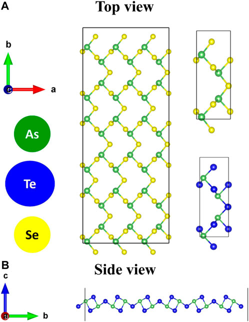
FIGURE 1. (A) Top view of a 3 × 2×1 supercell of As2S3 monolayer, Unit cell of As2S3 monolayer, Unit cell of As2Te3 monolayer and (B) Side view of As2Te3 supercell.
The calculated lattice vectors of As2S3 are a = 4.54 Å and b = 11.35 Å are comparable with previous theoretical results (a = 4.45 Å and b = 11.35 Å) (Mortazavi et al., 2020). However, they are higher than the experimental findings of 4.22 Å and 11.46 Å (Nobuo, 1954). The optimized lattice parameters of As2Te3 are a = 4.56 Å and b = 13.14 Å in this study compare well with previous theoretical results (a = 4.45Å b = 13.11Å) (Mortazavi et al., 2020). In reference (Liu et al., 2021b), the theoretical lattice parameters for monolayer As2S3 are a = 4.41 Å and b = 11.41 Å. In these references, the calculations are performed using Grimme’s DFT-D2 input DFT functional for vdW’s interactions, but in the present study, calculations are done differently using optPBE–vdW’s functional as mentioned in the computational methodology. So, the lattice parameters obtained in both the calculations vary slightly. The mechanical anisotropy for As2S3 has been studied theoretically (Liu et al., 2021b) and verified experimentally in reference (Šiškins et al., 2019). Similar anisotropic behavior has also been theoretically reported for As2Te3 in references (Mortazavi et al., 2020; Gao et al., 2021). The phonon dispersions of both monolayers have already been studied in references (Patel et al., 2020) and (Gao et al., 2021), exhibiting no imaginary frequencies. Hence, both the compounds are dynamically stable.
The electronic band structure and PDOS of As2S3 and As2Te3 monolayers are shown in Figure 2. Both structures show a semiconducting behavior with indirect bandgap values of 2.12 and 1.01 eV for As2S3 and As2Te3 as shown in Figures 2A, C, respectively. The CBM is located at the Gamma-point and the VBM is located at line between the Γ and X high symmetry points in the first Brillouin zone. Since the curvature near VBM and CBM is high or the gradient of PDOS near the fermi energy level for VBM and CBM is larger, the charge carriers are highly delocalized. Figures 2B, D show PDOS for As2S3 and As2Te3, respectively. From 2(b), As-pz orbital has maximum contribution to the conduction band near the Fermi-energy level, whereas S-px and S-py orbitals have most contribution to valence band states near Fermi level. Similarly, for As2Te3, Te–px and py orbitals have maximum contribution to the formation of valence bands near EF and the conducting bands are formed mainly from As-pz orbital.
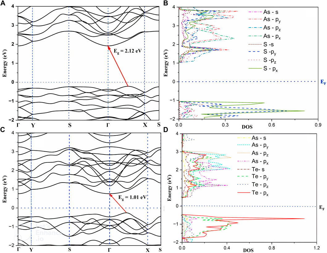
FIGURE 2. Electronic bandstructure and Project Density of States (PDOS) of As2S3 (A, B) and As2Te3 (C, D).
3.2 The effect of uniaxial and biaxial compressive and tensile strains on the electronic properties of As2X3 monolayers
In this subsection, the effect of strain on electronic properties of these monolayers is investigated in a comprehensive manner. Here, we consider compressive and tensile strain profiles of three different types: 1) Uniaxial strain along a_axis (Uni_a), 2) Uniaxial strain along b_axis (Uni_b), 3)Biaxial strain varying from −10% to +10% (compressive to tensile - biaxial). Figure 3 shows the graph of DFT energies versus strain for Uni_a, Uni_b and biaxial strains for (a) As2S3 and (b) As2Te3. It is clear from Figure 3 that the unstrained structure has a minimum or ground state, which indicates the most stable structure for both monolayers. In addition, the energy of the biaxial strain profile is always higher compared to uniaxial strain profiles. Also, the strain energies for Uni_a are consistently lower than that of Uni_b, implying that the structure undergoes maximum deformation along the a_axis. It is also important to note that the strain energies are always lower for As2Te3 as compared to As2S3, implying that As2Te3 can be deformed more easily.
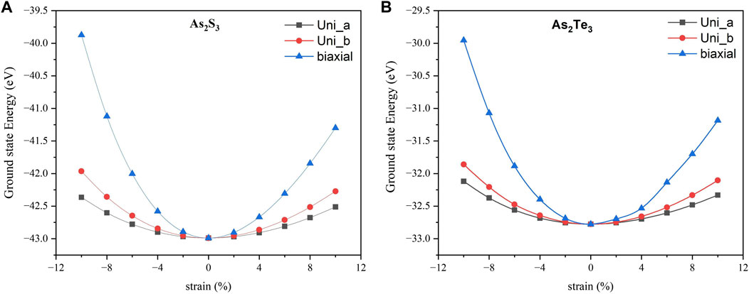
FIGURE 3. Strain energies Vs. strain percentage for (A) As2S3 and (B) As2Te3. Here, black squares represent Uni_a, red circles are for Uni_b and blue triangles are for biaxial strain profiles.
The most important property for optoelectronic applications is the bandgap, E.g., Figure 4 shows the effect of strain on the bandgap of As2S3 and As2Te3 monolayers. In this work, the effect of strain is studied in the range from −10% to +10% (with increasing bond length from −10% to +10% strain) as shown in Figure 4A, where the bandgap is maximized at Uni_a tensile strain of +8% for both As2S3 and As2Te3 monolayers. However, the bandgap maxima of As2S3 and As2Te3 monolayers are located at +4% and +2% for Uni_b tensile strain and biaxial tensile strain, respectively, see Figures 4B, C. A single example for Uni_b As2S3 case is considered in this study to understand this trend of the band structure changes (see Figure 5). As evident from Figure 5, the CBM shifts from Γ–point towards X-point, with increasing strain from −10% to +10%. This trend can be explained using the projected density of states for all strain profiles varying from −10% to +10%, see Supplementary Figures S1A–J. As evident from the Supplementary Figures S1A–C, for strain profiles −10%, −8% and −6%, the major contribution to CBM comes from As- py, As-pz and S-pz orbitals. On further reducing the compressive strain percentage for −4% and −2%, S- py orbital also contributes to CBM. Further going from the unstrained profile of 0% to +10%, As-px orbital also makes a significant contribution to CBM states near the Fermi energy level and it increases with increasing tensile strain. However, as we go from +2% to +10%, the contributions from As-py and S-pz orbitals cease to exist, see Supplementary Figures S1E–J, This results in the shift of CBM from Γ–point towards X-point.
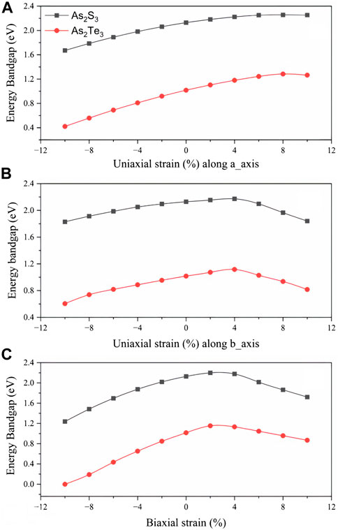
FIGURE 4. Effect of strain on electronic bandgap, E.g., (A) Uniaxial strain along a-axis, (B) Uniaxial strain along b-axis and (C) Biaxial strain. Squared symbol for As2S3 and circle for As2Te3.
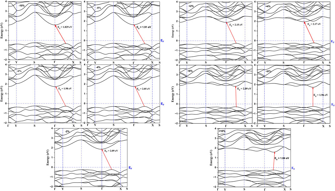
FIGURE 5. Demonstration of variation in electronic band-structure with strain for As2S3 Uni_b strain profile.
There is a transition from indirect to direct bandgap in As2S3 for uniaxial strain of 8% along b-axis (See the electronic band structure in Figure 5, whereas it retains its indirect nature for all the other strain profiles. Although, it seems that for +6% and +10%, the CBM and VBM are located closely along the Γ-X line, they are still indirect. Moreover, the system becomes metallic for the case of As2Te3 at biaxial compressive strain of −10% (Supplementary Figure S2) but is indirect semiconducting in all other strain profiles.
3.3 The effect of shear strain on the electronic properties of As2X3 monolayers
The employed strategy for selecting a limited number of shear strain profiles was as follows: Since the uniaxial strain along b-axis (Uni_b) resulted in a transition to direct bandgap semiconductor in As2S3 at +8%, it is kept fixed at this b-axis tensile strain, whereas that along the a_axis was varied from −2% to −10% for both compounds. As a result, As2Te3 transformed to a direct band gap material, whereas, As2S3 lost its direct bandgap nature. As indicated in Figures 6, 7 the comparative effect of shear strain in As2Te3 and As2S3 is shown for two cases: (0%, +8%) and (−10%, 8%), respectively.
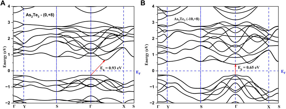
FIGURE 6. Demonstrating a transition to direct bandgap semiconductor in As2Te3 for a shear strain of (A, B) = (−10%, 8%) as shown in (B) as compared to Uni_b strain of +8% as shown in (A).
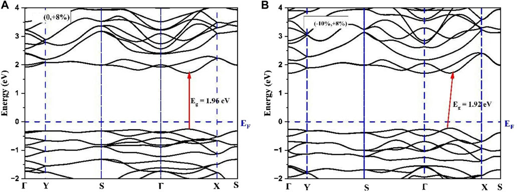
FIGURE 7. Demonstrating the loss of direct band gap nature from (A) (0, +8%) to (B) (−10%, +8%) in As2S3 monolayer.
3.4 Optical properties
In this section, the anisotropy in the optical absorption spectrum is discussed in the case of unstrained As2S3 and As2Te3 monolayers. As shown in Figures 8A, B, there is a strong anisotropic behavior as demonstrated in the absorption along XX and YY-direction. For the case of As2S3, there is a strong absorption in the UV range in the XX direction, which spans to some part of VIS spectrum as well. However, for the YY direction, the absorption peak is in the mid to near UV range and green, blue, violet and cyan parts of VIS spectrum. Similarly, for As2Te3 the absorption along both directions is in the near-IR, VIS and near-UV range. The optical bandgap can be calculated by drawing a tangential line to the absorption edge along XX direction, because the band gap is along the Γ- X line in the first Brillouin zone. Figures 8A, B show that the optical, E.g., for As2S3 and As2Te3 are 1.98 and 0.88 eV, respectively.
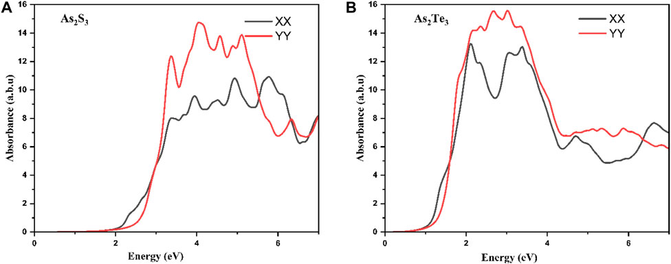
FIGURE 8. Optical absorption spectra for unstrained (A) As2S3 and (B) As2Te3 monolayers exhibiting anisotropic dependence along XX and YY direction.
The next step was devoted to study the effect of strain on the band gap. Here only the case of strained As2S3 monolayer along Uni_b (Uniaxial b-axis) is considered, since there was a transition to a direct bandgap behavior at +8% tensile strain as depicted in Figures 9A, B. It is also important to note that only the XX-direction is considered since the bandgap is located along the Γ-X line. The absorption band-edge is red shifted along with increasing compressive strain from 0% to −10% and is again red shifted for increasing tensile strain from 0 to +10%.
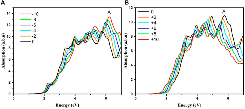
FIGURE 9. Effect of strain on optical absorption spectrum of (A) compressive strain and (B) tensile strain for Uni_b As2S3 monolayer.
The other important quantity is the static dielectric constant ε1 (0) and the effect of strain on it as shown in Figure 10A for As2S3 and Figure 10B for As2Te3. This is because it has the following relation with the bandgap:
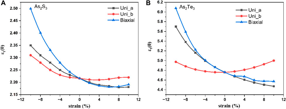
FIGURE 10. Static dielectric constant Vs. strain for monolayer As2S3 (A) and As2Te3 (B).
Hence, it can be said that opposite trends of decreasing bandgaps with increasing ε1 (0) should be observed. For all the three types of strain - Uni_a, Uni_b and biaxial strain, the minima occur at +8% tensile strain whereas, for As2Te3 minima occurs at 0% strain for Uni_b, however, it does not reach a minimum value for Uni_a and Biaxial strain. This shows that the plasma frequency plays an important role in all the above cases.
4 Conclusion
The effect of strain profiling on the optoelectronic performance of As2X3 monolayers is studied. One can expect a quantifiable increase in the, E.g., values on considering the above computationally extensive calculations like the use of hybrid functionals or GW-method implementation. The strain effect on the electronic and optical properties of As2X3 (X = S, Te) monolayers is investigated and presented. It was observed that for both monolayers, E.g., has maxima for at 8%, 4%, and 2% for uniaxial a-axis, uniaxial b-axis and biaxial strain profiles, respectively. There is a direct effect of strain on red shifting or blue shifting of the absorption spectrum depending on the material and strain profiling.
5 Scope statement
I am submitting the attached paper entitled “Effect of Strain Profiling on Anisotropic Opto-Electronic Properties of As2X3 (X = S, Te) Monolayers from First Principles,” by Andharia, et al. for your consideration of publishing it in Frontiers in Materials, section semiconductor materials and device. In this paper, we report on the effect of strain profiling on the optoelectronic performance of As2X3 monolayers. The band gap (E.g.,) values of these 2D materials were obtained by computationally extensive calculations. The strain effect on the electronic and optical properties of As2X3 (X = S, Te) monolayers is investigated and presented in this paper. It was observed that for both monolayers, E.g., has maxima for at 8%, 4%, and 2% for uniaxial a-axis, uniaxial b-axis and biaxial strain profiles, respectively. There is a direct effect of strain on red shifting or blue shifting of the absorption spectrum depending on the material and strain profiling. We believe this paper is very useful for the research community and we would like for you to give it a full consideration in publishing it in your journal.
Data availability statement
The raw data supporting the conclusion of this article will be made available by the authors, without undue reservation.
Author contributions
EA: Investigation, Methodology, Writing–original draft. HA: Investigation, Methodology, Software, Writing–review and editing. IE: Investigation, Methodology, Software, Writing–review and editing. BH: Investigation, Software, Supervision, Writing–review and editing. OM: Investigation, Supervision, Writing–review and editing.
Funding
The author(s) declare financial support was received for the research, authorship, and/or publication of this article. BH is supported by the MonArk Quantum Foundry that is funded by the National Science Foundation Q-AMASE-i program under NSF Award No. DMR-1906383.
Acknowledgments
The authors would like to thank Arkansas High Performance Computing Center (AHPCC), University of Arkansas, for the computing resources.
Conflict of interest
The authors declare that the research was conducted in the absence of any commercial or financial relationships that could be construed as a potential conflict of interest.
The author(s) declared that they were an editorial board member of Frontiers, at the time of submission. This had no impact on the peer review process and the final decision.
Publisher’s note
All claims expressed in this article are solely those of the authors and do not necessarily represent those of their affiliated organizations, or those of the publisher, the editors and the reviewers. Any product that may be evaluated in this article, or claim that may be made by its manufacturer, is not guaranteed or endorsed by the publisher.
Supplementary material
The Supplementary Material for this article can be found online at: https://www.frontiersin.org/articles/10.3389/fmats.2023.1325194/full#supplementary-material
References
Adam, M. L., Moses, O. A., Rehman, Z. u., Liu, Z., Song, L., and Wu, X. (2020). Band gap engineering of monolayer zrgete4 via strain: a first-principles study. Mater. Chem. Phys. 253, 123308. doi:10.1016/j.matchemphys.2020.123308
Dai, J., and Zeng, X. C. (2015). Titanium trisulfide monolayer: theoretical prediction of a new direct-gap semiconductor with high and anisotropic carrier mobility. Angew. Chem. Int. Ed. 54, 7572–7576. doi:10.1002/anie.201502107
Debbichi, L., Kim, H., Björkman, T., Eriksson, O., and Lebègue, S. (2016). First-principles investigation of two-dimensional trichalcogenide and sesquichalcogenide monolayers. Phys. Rev. B 93, 245307. doi:10.1103/PhysRevB.93.245307
Gajdoš, M., Hummer, K., Kresse, G., Furthmüller, J., and Bechstedt, F. (2006). Linear optical properties in the projector-augmented wave methodology. Phys. Rev. B 73, 045112. doi:10.1103/physrevb.73.045112
Gao, Z., Zhu, T., Sun, K., and Wang, J.-S. (2021). Highly anisotropic thermoelectric properties of two-dimensional As2Te3. ACS Appl. Electron. Mater. 3, 1610–1620. doi:10.1021/acsaelm.0c01100
Guo, Q., Pospischil, A., Bhuiyan, M., Jiang, H., Tian, H., Farmer, D., et al. (2016). Black phosphorus mid-infrared photodetectors with high gain. Nano Lett. 16, 4648–4655. doi:10.1021/acs.nanolett.6b01977
Huang, Y., Ning, J., Chen, H., Xu, Y., Wang, X., Ge, X., et al. (2019). Mid-infrared black phosphorus surface-emitting laser with an open microcavity. ACS Photonics 6, 1581–1586. doi:10.1021/acsphotonics.9b00096
Kistanov, A. A., Cai, Y., Zhou, K., Dmitriev, S. V., and Zhang, Y.-W. (2017). The role of h2o and o2 molecules and phosphorus vacancies in the structure instability of phosphorene. 2D Materials 4, 015010. doi:10.1088/2053-1583/4/1/015010
Klimeš, J., Bowler, D. R., and Michaelides, A. (2011). Van der waals density functionals applied to solids. Phys. Rev. B 83, 195131. doi:10.1103/physrevb.83.195131
Kresse, G., and Furthmüller, J. (1996). Efficient iterative schemes for ab initio total-energy calculations using a plane-wave basis set. Phys. Rev. B 54, 11169–11186. doi:10.1103/physrevb.54.11169
Kresse, G., and Hafner, J. (1993). Ab initio molecular dynamics for liquid metals. Phys. Rev. B 47, 558–561. doi:10.1103/PhysRevB.47.558
Kresse, G., and Joubert, D. (1999). From ultrasoft pseudopotentials to the projector augmented-wave method. Phys. Rev. B 59, 1758–1775. doi:10.1103/physrevb.59.1758
Lin, Y.-C., Komsa, H.-P., Yeh, C.-H., Björkman, T., Liang, Z.-Y., Ho, C.-H., et al. (2015). Single-layer res2: two-dimensional semiconductor with tunable in-plane anisotropy. ACS Nano 9, 11249–11257. doi:10.1021/acsnano.5b04851
Liu, X., Lv, B., Ding, Z., and Luo, Z. (2021a). External uniaxial compressive strain induced built-in electric field in bilayer two-dimensional As2S3 for photocatalytic water splitting: a first-principles study. Appl. Surf. Sci. 535, 147701. doi:10.1016/j.apsusc.2020.147701
Liu, X., Zhang, Z., Ding, Z., Lv, B., Luo, Z., Wang, J.-S., et al. (2021b). Highly anisotropic electronic and mechanical properties of monolayer and bilayer As2S3. Appl. Surf. Sci. 542, 148665. doi:10.1016/j.apsusc.2020.148665
Miao, N., Zhou, J., Sa, B., Xu, B., and Sun, Z. (2017). Few-layer arsenic trichalcogenides: emerging two-dimensional semiconductors with tunable indirect-direct band-gaps. J. Alloys Compd. 699, 554–560. doi:10.1016/j.jallcom.2016.12.351
Mortazavi, B., Shojaei, F., Azizi, M., Rabczuk, T., and Zhuang, X. (2020). As2S3, As2Se3 and As2Te3 nanosheets: superstretchable semiconductors with anisotropic carrier mobilities and optical properties. J. Mater. Chem. C 8, 2400–2410. doi:10.1039/C9TC05904K
Nobuo, M. (1954). The crystal structure of orpiment (As2S3) refined. Mineralogical J. 1, 160–169. doi:10.2465/minerj1953.1.160
Padilha, J. E., Miwa, R. H., and Fazzio, A. (2016). Directional dependence of the electronic and transport properties of 2d borophene and borophane. Phys. Chem. Chem. Phys. 18, 25491–25496. doi:10.1039/C6CP05092A
Patel, A., Singh, D., Sonvane, Y., Thakor, P. B., and Ahuja, R. (2020). Bulk and monolayer As2S3 as promising thermoelectric material with high conversion performance. Comput. Mater. Sci. 183, 109913. doi:10.1016/j.commatsci.2020.109913
Peng, X., Wei, Q., and Copple, A. (2014). Strain-engineered direct-indirect band gap transition and its mechanism in two-dimensional phosphorene. Phys. Rev. B 90, 085402. doi:10.1103/physrevb.90.085402
Perdew, J. P., Burke, K., and Ernzerhof, M. (1996). Generalized gradient approximation made simple. Phys. Rev. Lett. 77, 3865–3868. doi:10.1103/physrevlett.77.3865
Postorino, S., Grassano, D., D’Alessandro, M., Pianetti, A., Pulci, O., and Palummo, M. (2020). Strain-induced effects on the electronic properties of 2d materials. Nanomater. Nanotechnol. 10, 184798042090256. doi:10.1177/1847980420902569
Pumera, M., and Sofer, Z. (2017). 2d monoelemental arsenene, antimonene, and bismuthene: beyond black phosphorus. Adv. Mater. 29, 1605299. doi:10.1002/adma.201605299
Qiao, J., Feng, F., Wang, Z., Shen, M., Zhang, G., Yuan, X., et al. (2021). Highly in-plane anisotropic two-dimensional ternary ta2nise5 for polarization-sensitive photodetectors. ACS Appl. Mater. Interfaces 13, 17948–17956. doi:10.1021/acsami.1c00268
Sarkar, A. S., and Stratakis, E. (2020). Recent advances in 2d metal monochalcogenides. Adv. Sci. 7, 2001655. doi:10.1002/advs.202001655
Šiškins, M., Lee, M., Alijani, F., van Blankenstein, M. R., Davidovikj, D., van der Zant, H. S. J., et al. (2019). Highly anisotropic mechanical and optical properties of 2d layered As2S3 membranes. ACS Nano 13, 10845–10851. doi:10.1021/acsnano.9b06161
Tao, J., Shen, W., Wu, S., Liu, L., Feng, Z., Wang, C., et al. (2015). Mechanical and electrical anisotropy of few-layer black phosphorus. ACS Nano 9, 11362–11370. doi:10.1021/acsnano.5b05151
Wang, L., Kutana, A., Zou, X., and Yakobson, B. I. (2015). Electro-mechanical anisotropy of phosphorene. Nanoscale 7, 9746–9751. doi:10.1039/C5NR00355E
Wang, V., Xu, N., Liu, J.-C., Tang, G., and Geng, W.-T. (2021). Vaspkit: a user-friendly interface facilitating high-throughput computing and analysis using vasp code. Comput. Phys. Commun. 267, 108033. doi:10.1016/j.cpc.2021.108033
Wolverson, D., Crampin, S., Kazemi, A. S., Ilie, A., and Bending, S. J. (2014). Raman spectra of monolayer, few-layer, and bulk rese2: an anisotropic layered semiconductor. ACS Nano 8, 11154–11164. doi:10.1021/nn5053926
Xu, C., Zhang, J., Guo, Z., Zhang, S., Yuan, X., and Wang, L. (2021). A first-principles study on the electronic property and magnetic anisotropy of ferromagnetic crof and crocl monolayers. J. Phys. Condens. Matter 33, 195804. doi:10.1088/1361-648X/abe477
Keywords: first principles, strain engineering, anisotropic van der waal’s 2D materials, direct bandgap semiconductors, random phase approximation (RPA)
Citation: Andharia E, Alqurashi H, Erikat I, Hamad B and Manasreh MO (2024) Effect of strain profiling on anisotropic opto-electronic properties of As2X3 (X =S, Te) monolayers from first principles. Front. Mater. 10:1325194. doi: 10.3389/fmats.2023.1325194
Received: 20 October 2023; Accepted: 15 December 2023;
Published: 11 January 2024.
Edited by:
Yong Xie, Xidian University, ChinaCopyright © 2024 Andharia, Alqurashi, Erikat, Hamad and Manasreh. This is an open-access article distributed under the terms of the Creative Commons Attribution License (CC BY). The use, distribution or reproduction in other forums is permitted, provided the original author(s) and the copyright owner(s) are credited and that the original publication in this journal is cited, in accordance with accepted academic practice. No use, distribution or reproduction is permitted which does not comply with these terms.
*Correspondence: M. O. Manasreh, manasreh@uark.edu