Optimization of the position of TaOx:N-based barrier layer in TaOx RRAM devices
 Pramod Ravindra1
  Maximilian Liehr1 Rajas Mathkari1 Karsten Beckmann1,2 Natalya Tokranova1
  Nathaniel Cady1*
- 1College of Nanotechnology, Science, and Engineering, University at Albany, Albany, NY, United States
- 2New York Center for Research, Economic Advancement, Technology Engineering and Science, Albany, NY, United States
Resistive Random-Access Memory (RRAM) presents a transformative technology for diverse computing and artificial intelligence applications. However, variability in the high resistance state (HRS) has proved to be a challenge, impeding its widespread adoption. This study focuses on optimizing TaOx-based RRAMs by strategically placing a nitrogen-doped TaOx barrier-layer (BL) to mitigate variability in the HRS. Through comprehensive electrical characterization and measurements, we uncover the critical influence of BL positioning on HRS variability and identify the optimal location of the BL to achieve a 2x lowering of HRS variability as well as an expanded range of operating voltages. Incremental reset pulse amplitude measurements show that the TaOx:N maintains a low HRS variability even at higher operating voltages when the position of the BL is optimized. Our findings offer insights into stable and reliable RRAM operation, highlighting the potential of the proposed BL to enhance the functionality of TaOx-based RRAMs and elevate overall device performance.
1 Introduction
In the rapidly evolving landscape of artificial intelligence (AI) and machine learning (ML) technologies, the quest to revolutionize various aspects of modern society, encompassing all available avenues to improve quality of life, continues to gather momentum. However, the AI/ML systems available at present grapple with significant constraints, largely due to their reliance on large-scale processing systems and computationally intensive training methods executed using conventional von Neumann computing architecture. These constraints become even more pronounced as the demand for real-time, high-precision cognitive operations are choked by the increasing density of raw data and increasingly complex models, which require fast and numerous cycles of data exchange between storage and computation modules.
Recent investigations into the workings of the human brain have culminated in models that elucidate its underlying computational principles. Guided by these principles, a new generation of materials, devices, circuits, and systems have been built that aim to emulate the intricate functionality of the brain. This paradigm shift, known as neuromorphic computing, is based on a neural-like computing architecture poised to drive the future of AI/ML systems. Neuromorphic chips, underpinned by unified memory and in-memory computing technologies, have emerged as a promising solution capable of expediting AI/ML applications, while being free from the latency and energy constraints associated with data movement in the conventional von Neumann architecture.
In this context, neuromorphic systems are uniquely positioned to undertake real-time information analysis even with a constant input of large volumes of data. On the hardware front, materials, and devices such as memristors are garnering substantial attention for implementing electronic neurons and synapses, harnessing their key attributes such as non-volatility, low latency, scalability, and energy efficiency. In particular, RRAM has emerged as a crucial technology for these applications (Zhu et al., 2020a; Zahoor et al., 2020).
Unlike traditional memory types, RRAM stores data by changing the resistance of a material between high resistance state (HRS) and low resistance state (LRS). RRAMs offer numerous advantages such as high endurance, fast switching speeds, and scalability, making them an attractive choice for next-generation memory devices. Among the various types of RRAM devices that are known, oxide-based RRAM devices have gained significant attention due to their compatibility with complementary metal-oxide-semiconductor (CMOS) processes widely used in semiconductor fabrication (Dittmann et al., 2021). RRAMs based on two materials in particular, HfOx and TaOx, are especially attractive due to their high dielectric constants, low energy of oxygen vacancy formation, and the familiarity of these materials to the semiconductor fabrication ecosystem (Clima et al., 2014; Zhu et al., 2020b).
Despite significant effort, the widespread integration of RRAM across diverse applications is impeded by its intrinsic device variability (Grossi et al., 2017; Liehr et al., 2022a; Liehr et al., 2022b). It is well known that higher resistance values in HRS are accompanied by higher variation, as corroborated by theory (Guan et al., 2012) and empirical investigations. (Liehr et al., 2022a). The random nature of ionic movement within the filaments in RRAM devices (Miranda et al., 2012) necessitates the incorporation of system-level interventions and error-correction to circumvent the device variation, contributing to sizeable overheads from complex programming controllers and write/verify iterations (Solanki et al., 2023).
The physical source of the resistance variability in the HRS is the variability in the size of the filament gap (Guan et al., 2012; Larentis et al., 2012). In the LRS, the filament is continuous and offers a conduction path between the electrodes. However, when ruptured during the reset process which takes the device into the HRS, electrons need to hop across the gap in the filament to reach the anode (Xu et al., 2008; Lee et al., 2009; Kwon et al., 2010). Since the tunneling probability across an insulating region depends exponentially on the gap size, changes in the gap size strongly affect the resistance in the HRS (Bersuker et al., 2010; Yu et al., 2011; Huang et al., 2013). The size of the filament gap is determined by the random walk of oxygen ions within the amorphous switching layer, and their recombination with vacancies which is a stochastic process (Ambrogio et al., 2014). This stochasticity may be pinned as the primary source of the cycle-to-cycle and device-to-device variability in HRS resistance (Guan et al., 2012). Therefore, controlling material parameters associated with vacancy generation and annihilation as well as oxygen ion motion, are recognized as a viable ways to control HRS variability. Considering this, several material and device-scale solutions have been proposed to address the challenge, with the general goal of controlling the filament size and/or the filament gap.
Of these, extrinsic doping has emerged to be the most popular approach to change the vacancy generation and recombination statistics. Implanting Al (Qin et al., 2021) or Zr (Kempen et al., 2021a) atoms in TaOx switching layer to form a region within the TaOx layer with high dopant concentration was shown to reduce the vacancy formation energy, while increasing the barrier for diffusion of oxygen ions. The combined effect is to improve endurance and uniformity of the HRS state (Kempen et al., 2021a) as well as the reset voltage (Qin et al., 2021). It has also been shown in TaOx devices that localized doping results in larger gains in uniformity compared to uniform doping of the switching layer (Kempen et al., 2021b), which was attributed to stochasticity in dopant distribution and activation that can negate gains due to doping. Precursors used during ALD deposition of the switching material has also been demonstrated to strongly affect the HRS variability, since it affects defect energetics and therefore the reaction rates of the vacancy generation/annihilation processes (Hazra et al., 2019).
Wei et al. recently proposed a solution that may be used in conjunction with other solutions to further improve the variability in the device (Chen et al., 2021). Through the introduction of an SnO ‘oxygen stopping layer’ in the HfOx switching layer, the work reported a lower variability in the HRS compared to a device without the SnO layer. This reduction in HRS variability was attributed to a reduced variability of the filament gap when it resides within the SnO layer, compared to when it resides in HfOx.
While such a layer to impede oxygen ion motion has been implemented and demonstrated for HfOx based RRAMs, a similar layer is yet to be demonstrated in TaOx-based RRAMs. In this study, we implement a barrier layer (BL) within a TaOx RRAM which impedes oxygen ions and investigated the optimal position of the BL to minimize the variability of the HRS. In TaOx, several materials have been investigated as dopants both in the context of RRAMs and otherwise with the aim of modifying the properties of the filament or the dynamics of filament formation and/or rupture (Kempen et al., 2021b; Palhares et al., 2021; Qin et al., 2021). Nitrogen doping of oxide compounds has been employed to improve RRAM switching properties using various switching materials, including TaOx. Devices with TaOx:N switching layers have shown lower LRS variability in multi-level cells (Misha et al., 2015). However, they also show higher non-linearity when tested for potentiation and depression (Kim et al., 2022), highlighting the need to confine the region of constrained oxygen motion within the switching layer (Wang et al., 2018). Given the CMOS compatibility of TaOx:N, and the possibility of doping TaOx by introducing nitrogen into the gas mixture during deposition, N-doped TaOx is chosen as the material for the BL.
To determine the optimal position of the BL, we fabricated different device stacks including the BL layer at different positions within the switching layer and completed extensive electrical characterization of these RRAM devices. Through comprehensive pulsed IV, endurance, and incremental reset amplitude measurements, we assessed consistent trends in both device-to-device and cycle-to-cycle variability as the position of the BL changes relative to the oxygen exchange layer (OEL). Notably, we find that when the BL is positioned within a range of distances from the OEL, the HRS variability is up to 2x lower compared to other locations, allowing us to deduce both the optimal position of the BL as well as the position of the filament gap. Furthermore, in devices with a TaOx:N BL, regardless of the position of the layer, the device supports an extended range of operating voltages, extending the applicability of TaOx:N layers in TaOx-based RRAM devices.
2 Experiment
RRAM devices containing TaOx as the switching layer were fabricated on a bottom electrode template built using 65 nm CMOS technology with the process flow modified to integrate RRAM devices between the M1 and M2 layers. The template contains an exposed TiN bottom electrode connected to a W bottom electrode contact pad, along with an in-built series resistance designed to protect the RRAM device. The exposed TiN electrode is 50 nm in diameter, which forms the bottom electrode of the RRAM device.
On top of this template, a TaOx/TaOx:N/TaOx/Ta/Ir stack was deposited using sputtering using the Kurt Lesker PVD 75 tool. For the deposition of TaOx switching layer, reactive RF sputtering was used with a metallic Ta target (99.999% pure, Kurt Lesker) in the presence of oxygen. The partial pressure of oxygen (pO2) was maintained at 0.23 mTorr during TaOx deposition, while the total deposition pressure was 3 mTorr. The remainder of the gas flow was from Ar. RF power of 125 W was used during deposition. Before the deposition, the chamber was pumped down to a base pressure <10−6 Torr and backfilled with Ar. The target was cleaned for 600 s in pure Ar before introduction of O2 into the chamber. After introducing O2, a 90 s stabilization time was set for the plasma composition to stabilize, before opening the substrate shutter for deposition.
For the BL deposition, nitrogen incorporation was achieved by introducing N2 into the gas mixture during reactive sputtering. Additionally, to further reduce the mobility of oxygen atoms within the stopping layer, the BL was made more oxygen rich, by maintaining a higher pO2 of 0.45 mTorr. During the deposition, pN2 was maintained at 0.11 mTorr, which was the lowest available partial pressure for N2, while the total chamber pressure was 3 mTorr. The rest of the parameters were identical to TaOx deposition. Depending on the required thickness, deposition times were chosen based on prior thickness calibration experiments, for the top SL, bottom SL and the TaOx:N BL layers.
A 5 nm thick Ta layer was used as the oxygen exchange layer (OEL). Ta was deposited using DC sputtering in pure Ar plasma using a different Ta metallic target (99.999% Kurt Lesker) to avoid contamination of the OEL with oxygen. The chamber pressure was maintained at 3 mTorr and the DC power was set to 100 W. This layer was capped with 5 nm of Ir, to protect the device stack from atmospheric oxidation, when the chamber is opened to replace the targets. Ir was deposited at 50 W using DC sputtering. Finally, a 50 nm thick W top electrode is deposited using DC sputtering at a power of 100 W.
These blanket layers deposited on the template were then lithographically patterned using an OAI Mask aligner to mask top electrodes with 60 μm × 60 µm contact pad pattern. Following lithography, the device structure was defined by etching down the exposed regions using plasma-etching using an SF6 + O2/SF6 + O2 + Ar based, etch recipe. The finished devices were then annealed to activate the N as dopants in the BL. Four structures were fabricated, with different positions of the BL. Samples A, B, and C all had a 10 nm switching stack. Sample D had a switching stack thickness of 8.7 nm. A control device with 10 nm SL but without a BL and one with a BL similar to structure B but made of undoped TaOx deposited at 0.45 mTorr were also fabricated.
10 nm thick TaOx:N blanket films with Ir capping layer were deposited on silicon wafer samples using the same PVD parameters as those used during device fabrication. These samples were used for XPS to determine the annealing temperature. The as-deposited films were annealed to two different temperatures: 300°C and 500°C, for 30 min, in a vacuum of 10−7 mTorr. XPS measurements were performed using an Al Kα source with 1486.6 eV equipped with charge compensation and a monochromator. The XPS spectra were acquired with a step size of 0.05 eV. The obtained spectra were calibrated using Ir 4f7/2 peak at a binding energy of 60.8 eV.
Electrical characterization was performed using a probe station integrated with an Agilent B1530A. To protect the RRAM device from a capacitive overshoot current, these devices were connected to an external transistor during electrical characterization. The gate voltage of the external transistor was set such that the saturation current is 120 μA, which serves as the compliance current during the forming and set operation. There is no current compliance during the reset operation. Voltages were applied to the W top electrode while the bottom electrode was connected to ground throughout the test. In this configuration, a positive (negative) voltage applied to the top electrode causes the device to switch to the low (high) resistance state. All devices under test were subjected to an initial forming step using a 10 ms long 5 V pulse, followed by 10 pulsed IV sweep with a rise/fall time of 100 us, to confirm that they were switching. The devices were then cycled through 1000 reset-set cycles, The applied voltages during endurance tests were ±2.2 V. followed by incremental reset pulse amplitude measurements. For each structure, 10 devices were measured to ensure the consistency of the results.
3 Results
TaOx:N layers were deposited by introduction of N2 in the gas mixture during reactive RF sputtering of TaOx layers using a metallic Ta target. Activation of nitrogen dopants in these films is a critical step in achieving the desired properties, which was achieved through annealing. To determine the effect of annealing temperature on the activation of nitrogen dopants in TaOx films, X-ray Photoelectron Spectroscopy (XPS) measurements were performed.
XPS spectra of Ta 4f and N 1s were analyzed to identify the effect of annealing temperature. Ta 4f and N 1s XPS spectra are presented in Figure 1. The Ta 4f spectrum exhibits a 4f5/2 – 4f7/2 doublet structure with a spin-orbit splitting of 1.91 eV. During peak fitting, a GL30 line shape was employed for all peaks, applying a forced spin-orbit split of 1.91 eV. Furthermore, the ratio of the areas of 4f5/2 and 4f7/2 peaks was constrained to 3:4, with equal Full Width at Half Maximum (FWHM). The determination of chemical shifts and oxidation states relied on literature averages available in the NIST XPS database (Wagner, 1990).
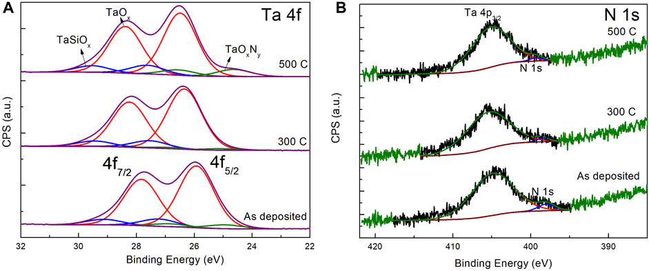
Figure 1. XPS spectra for Ta 4f (A) and N 1s (B) from TaOx:N under different annealing temperatures.
The XPS spectra obtained at each temperature were analyzed by fitting them to three sets of peaks. In the as-deposited sample, the main Ta 4f7/2 peak appeared at a binding energy of 25.9 eV, indicating the presence of Ta2O5-x. A set of peaks at a higher binding energy was observed, attributed to the TaSi2Ox phase, likely resulting from reactions between the native silicon oxide on the surface of the Si wafer and the deposited Ta and O species. Additionally, a set of peaks at a lower binding energy, with the Ta 4f7/2 peak at 24.9 eV, which may be attributed to sub-oxide species (Misha et al., 2015).
Upon annealing at 300°C, the main oxide peaks shifted higher by 0.4 eV, suggesting chemical shift resulting from further oxidation with unincorporated oxygen atoms in the film. Peaks at a lower binding energy of 24.9 eV (4f7/2) appeared with lower intensity. The peak position of TaOxNy is expected to lie between that of Ta2O5 at 26.6 eV and TaN at 23 eV (Shin et al., 2008; Misha et al., 2015). As the annealing temperature increased to 500°C, the film oxidized further as evidenced by the increase in the 4f7/2 peak position by 0.2 eV. The peaks corresponding to TaOx:N are not apparent at a lower binding energy, indicating nitridation (Misha et al., 2015).
Figure 1B shows the XPS spectra for N 1s. The Ta 4p peak overlaps significantly with the N 1s peaks. The nitrogen peak position and intensities exhibited a notable dependence on the annealing temperature. Since the nitrogen concentration in the films is relatively low, the Ta peak dominates the XPS spectrum. As a result, the N 1s peak appears as a hump, which may be properly identified only after peak fitting. By utilizing an unconstrained GL30 peak shape, the N 1s peak energies were determined at different annealing temperatures. In all samples, the observed N 1s peak positions are higher than that of the N1s XPS peak in TaN at 396.3 eV, suggesting the presence of oxynitride species in the samples (Shin et al., 2008). In the as-deposited state, the N 1s peak was detected at 398 eV. Upon annealing at 300°C, the N1s peak shifted slightly higher to 398.6 eV, and at 500°C, it further increased to 399.2 eV, indicating improved dopant activation (Cristea et al., 2019). Guided by the XPS results, we choose 500 °C as the preferable annealing temperature for the films. All devices studied in this work were annealed to 500°C for 30 min.
Detailed electrical characterization was performed to characterize the electrical behavior of the devices. Four device structures were fabricated with different positions of the BL. Since the devices were annealed at 500°C for 30 min, it may be expected that the nitrogen atoms present in the BL will also have diffused outwards into the nominally undoped TaOx regions. Figure 2 shows a schematic of the fabricated structures, with the highest nitrogen concentration at the nominal position of the BL with a gradient extending outwards. The structures were fabricated using the bottom electrode and contain an inbuilt resistor creating 1R–1R (one resistor in series with one RRAM) devices. Figure 3 shows the DC switching parameters for the different structures. For the set process, all structures demonstrate a similar median voltage, suggesting comparable energy requirements for the set transition. The distribution of reset voltages for structures B and D is narrower than that of A and C, pointing to a more consistent reset process. This could suggest an enhanced control over the filament gap in these structures, potentially due to the layer positioning and the physical characteristics of the stack.
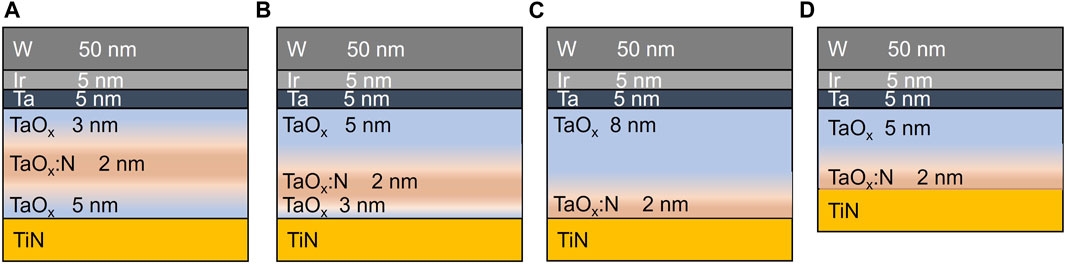
Figure 2. Schematic showing the cross sections of the four device structures (A–D) that were fabricated to determine the optimal location of the oxygen stopping layer in TaOx based RRAM devices.

Figure 3. DC switching parameters for the four different device structures (A–D): Set, reset and forming voltages.
The forming voltages also shows notable differences between structures. Structure D, with its thinner switching stack, has a lower median forming voltage compared to the other structures, which aligns with the expectation that a thinner stack would require less energy to form the conductive filament. The trend observed suggests that the farther the blocking layer is from the OEL, the lower the energy required for the forming process. This can be related to the displacement of oxygen ions: a thicker filament, closer to the OEL, implies more ions to displace, thereby increasing the necessary forming voltage.
Endurance measurements were performed to assess the stability of device switching and to evaluate the cycle-to-cycle variability for the four samples. Devices were not cycled until failure, but instead cycled for a uniform 1000 cycles for direct comparison. This allowed us to compare the variability among the samples and investigate the influence of the position of the barrier layer (BL) on device performance. Representative endurance plots obtained for all four structures and the pulse IV measurements included as insets, are shown in Figure 4. Endurance plots for 10 devices are shown in Supplementary Figure S2. Both the pulse IV measurements and endurance plots exhibited a memory window sufficient to discern between LRS and HRS indicating successful switching. Structures A and C demonstrated higher resistance in the HRS compared to structures B and D. Furthermore, these structures exhibited a higher spread in HRS resistance, featuring a reducing trend in HRS for structure A and intermittent “spikes” for structure C. These irregular variations caused the memory window to vary significantly before returning close to the median value. On the other hand, structures B and D showed slightly lower HRS resistance compared to A and C, while any irregularity was absent. The distribution of HRS values for structure D was particularly tight around the median value of approximately 100 kΩ, without any intermittent spikes. Across all structures, the LRS value remained closely distributed around 15 kΩ.
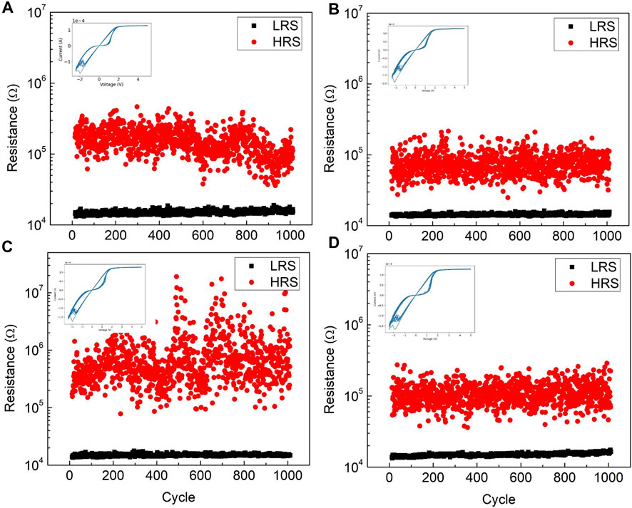
Figure 4. Endurance and Pulse IV plots for device structures (A–D). Inset in each show 10 pulsed IV sweeps collected before the endurance measurements.
In addition, we explored the impact of the presence and composition of the BL on device performance. The negative control samples were identical to sample B but without N incorporation, i.e., with a BL consisting solely of TaOx deposited at pO2 of 0.45 mTorr. The negative control sample without a BL both exhibited inferior behavior in terms of memory window and variability in both HRS and LRS states when compared to the four test samples. Endurance plots for these device structures are illustrated in Supplementary Figure S3. This highlights the role of not just incorporating the BL but also the incorporation of nitrogen in the BL.
To assess the cycle-to-cycle variability across all devices tested, we analyzed the endurance data of multiple devices rather than just one representative device. While the representative device displayed larger HRS variability, it is also clear that there were several outliers. Therefore, to evaluate the cycle-to-cycle variability and compare the performance of the four structures, we sought a robust measure that could effectively capture the spread of the HRS values while being less influenced by outliers. We adopted the Quartile Coefficient of Dispersion (QCD) as a more robust parameter to assess HRS variability (Bonett, 2006).
The Quartile Coefficient of Dispersion (QCD) is calculated as follows:
where Q1 and Q3 are the first and third quartiles, respectively, of the dataset. A lower QCD value indicates a tighter distribution around the median, suggesting reduced variability, while a higher QCD value implies a more dispersed dataset, indicating higher variability.
The advantage of using QCD lies in its robustness against outliers, making it particularly suitable for our analysis, where we observed outliers causing momentary narrowing or increase in the HRS resistance and memory window. QCD is less sensitive to extreme values that might skew conventional measures like standard deviation (σ) or the popular coefficient of variation σ/µ where µ is the mean of the dataset. This ensures that QCD provides a more reliable representation of the true variability in HRS across the devices. In our analysis, for better representation, the QCD values are multiplied by 100 to display percentage values.
In Figure 5A, we present a box plot of QCD values obtained from 10 devices, illustrating the median variability observed among the tested devices. The individual data points contributing to the box plots are also shown on the plots. Each QCD value contributing to the box plot is the coefficient computed for 1000 reset-set cycles. This representation allows us to observe the overall trend in cycle-to-cycle variability. The box plot of QCD values reinforces the conclusions drawn from the endurance plots in Figure 4, providing a clearer picture of the impact of the oxygen stopping layer (BL) position on HRS variability.
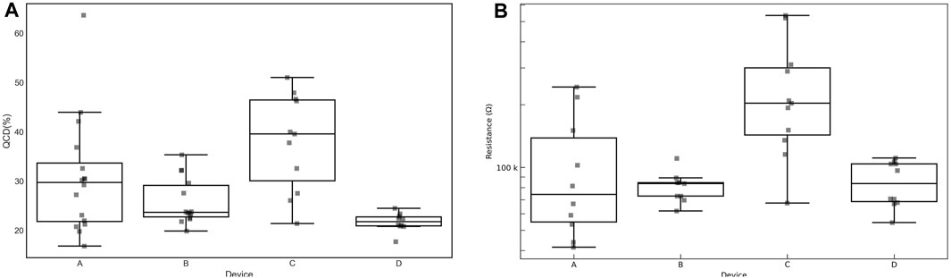
Figure 5. QCD (A) and HRS (from 1000 cycles) (B). The x label shows the corresponding structure. Device structures B and D show lower variability (lower QCD as well as lower spread in HRS).
Upon examining the median QCD values, we found that samples A and C exhibited larger variability compared to samples B and D. Sample D, in which the BL was deposited right on top of the bottom electrode, displayed the least variability with a median QCD of 20%, which was half that of sample C, which had the highest variability of all structures tested. Additionally, the spread in QCD values across devices indicated that in structures B and D, the low cycle-to-cycle variability was consistent across the die, unlike structures A and C. This suggested that device-to-device variability is also low in all the structures tested with the QCD tightly distributed around the median value. In contrast, structures A and C exhibited higher median as well as spread in QCD values, indicating higher device-to-device variability across devices.
To gain further insights into the device-to-device variability, we constructed box plots of the median HRS values in Figure 5B. In this representation, where only the median HRS values from 1000 cycles of each device were considered, information regarding cycle-to-cycle variability is lost but it provides a clear illustration of device-to-device variability. Structures A and C displayed higher median HRS values compared to structures B and D, which show tighter distributions in their median HRS values, suggesting that the variation across devices (i.e., device-to-device variability) was lower in structures B and D compared to structures A and C. This corroborates the observations made using QCD analysis.
These observations allow us to delve into the influence of the BL position relative to the top electrode (TE). As the BL was positioned at various distances from the TE, distinctive trends in HRS variability emerged. When the BL was located 3 nm away from the TE (structure A), the HRS variability was initially high. As the BL location moved away from the TE by 2 nm (structure B), the HRS variability decreased, along with a reduction in the HRS magnitude. However, when the BL was positioned further away by 3 nm (structure C), touching the bottom electrode, the HRS magnitude and variability increased. Moving both the BL and the bottom electrode closer to the TE by 2 nm (structure D) resulted in a decrease in HRS magnitude and variability, similar to that observed in structure B. These results suggest an “optimal” region for the BL relative to the top electrode: approximately between 5 and 7 nm from the TE.
To comprehensively investigate the impact of the BL on device behavior, we conducted incremental reset pulse amplitude measurements (IRPA). In this set of experiments, we used the same positive set pulse voltage while progressively varying the negative reset voltage from −1.5 V to −4 V in increments of 0.1 V. Through this approach, we subjected the devices to 100 reset-set cycles at each voltage increment.
The experiment was designed to probe the influence of increasing Vreset voltage on the HRS variability. As Vreset was increased, oxygen ions would be compelled to traverse beyond the BL. The higher electric field under a higher Vreset would induce greater ion motion, potentially leading to increased variability in the HRS due to an “overshoot” out of the filament gap (Lee et al., 2009).
In Figure 6, we present plots showing the HRS and LRS distributions obtained during the IRPA measurements for the four structures. Supplementary Figure S5 shows the IRPA plots for four devices per structure. The observations revealed distinct trends, shedding light on the dynamic response of the devices to changing reset voltages. For structure A, we noted a rapid surge in HRS variability around −2 V, marking the onset of device switching and the emergence of a memory window. Both the HRS value and its variability swiftly increased, characterized by a broad spread in HRS values (Figure 6A). Beyond −3.3 V, the HRS and LRS began to converge, with the LRS increasing significantly causing the memory window to reduce drastically. As the memory window reduced below 2, the device is considered to have failed as it becomes difficult for the states to be discerned reliably. In contrast, structure C exhibited a more gradual rise in HRS (Figure 6C), accompanied by steady HRS variability as the resistance escalated by over an order of magnitude from below 100 kΩ to over 1 MΩ. This trend peaked at −2.7 V, followed by a reduction in HRS and a slight increment in variability until −3.3 V, at which point both HRS and LRS again converged into an intermediate value followed by device failure. Structure B displayed an onset of switching around −2 V, and a gradual increase in HRS until −3.2 V (Figure 6B). There was no notable increase in the spread in HRS. Subsequently, a slight reduction in HRS was observed at −3.3 V, followed by failure. In structure D, the HRS variability remained consistent as the device switched around −2 V, while the HRS itself exhibited slow and steady growth, the most gradual of the four structures tested (Figure 6D). Unlike all the other structures, even at the maximum voltage of −4 V, neither the LRS nor the HRS collapsed, and the devices maintained a memory window, indicating operational integrity until the extreme voltage.
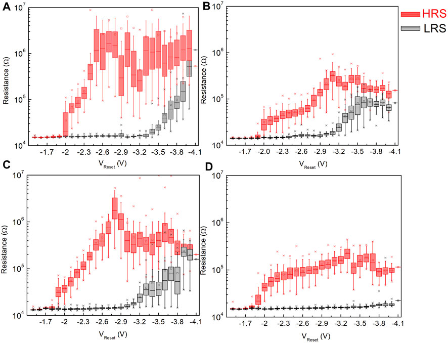
Figure 6. Incremental reset pulse amplitude measurements for device structures (A–D).
4 Discussion
This study has enabled us to elucidate the effect of BL position on cycle-to-cycle variability of the HRS for TaOx RRAM. The results from the experiments, endurance testing, and incremental reset pulse amplitude measurements also provide valuable insights into the behaviour of the BL and its impact on device performance.
The investigation into the effect of incorporating a BL at different locations in a TaOx switching layer stack reveals a clear interpretation based on its relative position within the device structure. The RRAM switching mechanism is characterized by the formation and disruption of conductive filaments. These filaments have been effectively conceptualized using an hourglass model, offering insights into the underlying filamentary dynamics as outlined in several studies (Balatti et al., 2013; Syu et al., 2013; Degraeve et al., 2014; Zhang et al., 2022). This model simplifies the filament into a structure comprising two reservoirs connected by a central constriction analogous to the neck of an hourglass. Ref (Degraeve et al., 2014) explains the emergence of the hourglass structure, detailing the kinetic, structural, electrical, thermal, and stochastic aspects of the filament.
Initially, in a pristine RRAM device, the dielectric is devoid of any conductive filament, with oxygen vacancies being sporadically distributed throughout the dielectric material, as shown in Figure 7A. The forming process introduces a differential in the concentration of oxygen vacancies, higher near the OEL and progressively diminishing towards the BE. This gradient is primarily attributed to redox reactions at the OEL/dielectric interface. Concurrently, a number of oxygen vacancies migrate towards the BE, where they accumulate at the dielectric/BE interface Figure 7B, panels (i) and (ii). This dual effect of vacancy migration culminates in an oxygen vacancy profile with a higher concentration adjacent to the OEL/dielectric interface, tapering off towards the BE but surging again near the dielectric/BE interface, depicted in Figure 7B, panel (iii). The result is a distinct region where vacancy concentration is at its minimum, creating a constriction point similar to the neck of an hourglass. Once a current path is established, the filament is strengthened through further migration of vacancies as seen in panel (iv). Factors influencing the precise location of this constriction include the dielectric’s thermal properties, ionic mobility, and resistance of the filament. This arrangement of vacancies creates a conduction path from the TE to the BE, and the device is programmed to the LRS state.

Figure 7. Emergence of the hourglass shape of the filament in the (A) Pristine device and through (B) forming (C) Reset and (D) Set processes.
During the reset phase, this constriction becomes the filament’s most resistive segment, heating considerably due to Joule heating when a reset pulse is applied. This localized heating enhances the mobility of the vacancies, causing them to vacate the constriction creating a gap in the filament and thereby transitions the device into a high-resistance state, as demonstrated in Figure 7C. Conversely, the ‘set’ process reverses this phenomenon. Here, vacancies migrate from the top reservoir towards the lower one, re-establishing the conductive pathway and shifting the device back to a low-resistance state, illustrated in Figure 7D.
We use the position of the BL relative to the filament gap found in HRS to interpret the effect of different positions of the BL on the HRS variability. In structure A, the BL is positioned closer to the OEL (3 nm) and farther from the bottom electrode (5 nm). The filament gap resides within the region outside the BL towards the BE. After annealing, it may be expected that nitrogen diffused into the regions above and below the initial position of the BL. The concentration of nitrogen atoms may be expected to not be high enough to cause any significant gains in HRS variability. This configuration is characterized by high cycle-to-cycle variability, high device-to-device variability, as well as a higher HRS value, due to large filament gap formed (Chen et al., 2021) in a predominantly undoped region of TaOx. The large filament gap is also expected to be a result of greater mobility of oxygen ions in this region compared to the BL. In IRPA measurements, HRS resistance and variability both swiftly increased due to a clear overshoot of the oxygen ions. In structure B, where the BL is closer to the BE, there is a stronger overlap between the region with high nitrogen concentration as well as the filament gap, resulting in stable device operation. The cycle-to-cycle variability is lower and so is the HRS, due to smaller filament gap. In IRPA measurements, a voltage regime is seen where the HRS rises slowly compared to structure A, but the variability is lower.
Moving the BL further away from the OEL towards the bottom electrode (as in structure C) leads to an extension of the filament gap into the TaOx layer towards the OEL, causing higher variability, similar to structure A. The cycle-to-cycle variability is higher compared to sample B. In IRPA measurements, the rise in HRS resistance is gradual and the HRS variability is steady as the HRS resistance increases. This may be attributed to the reduced mobility of oxygen atoms in the nitrogen-rich region impeding the filament gap from rapidly increasing by constraining the motion of oxygen ions, leading to a slower rise in HRS resistance as the Vreset increases. Finally, relocating both the BL and the BE closer to the OEL restores stability by keeping the filament gap within the BL. This structure is also observed to be the one with least HRS variability as the filament gap coincides with the region of highest nitrogen density, as nitrogen is not expected to diffuse into the TiN bottom electrode. These observations are summarized in Figure 8. This interpretation underscores the critical role of precise BL placement for achieving optimal device behaviour. Additionally, structure D stands out with exceptional operational stability even at high voltages, attributed to the interaction between TaOx:N and the TiN bottom electrode preventing defects from drifting into the switching layer. This observation emphasizes the potential of the proposed device architecture for robust and high-performance memory applications.
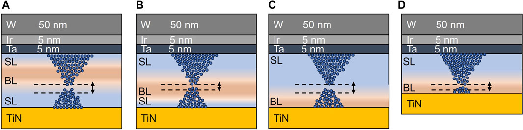
Figure 8. Interpretation of BL effect on HRS variability for the four different device structures (A–D).
Nitrogen doping emerges as a pivotal strategy for enhancing BL performance. It is known from prior literature that nitrogen incorporation restricts oxygen ion migration and localizes oxygen ions near the filament gap (Syu et al., 2013), thereby reducing the mobility of oxygen within the BL. Moreover, nitrogen occupies vacancy sites, limiting available sites for oxygen atom migration and contributing to reduced oxygen mobility (Umezawa et al., 2005; Xie et al., 2012). These two factors reinforce the effectiveness of the TaOx:N BL as a robust barrier. The successful integration of nitrogen doping serves as a key factor in achieving consistent and stable device operation.
The impact of BL configuration on device performance is further underscored by the identification of an optimal region for BL placement, approximately between 5 and 7 nm from the OEL. This range corresponds to a stable configuration where the filament gap predominantly resides within the nitrogen rich BL, leading to reduced variability and consistent device behavior. It should be noted that the shape of the filament depends on the device structure–i.e., the choice of the OEL, top and bottom electrodes and the composition of the switching layer (Zhang et al., 2022). Another important finding from this work is that the location of the BL for optimum performance being 5–7 nm from the OE L implies that the filament gap occurs in this region. Designing experiments such as these, with varying positions of the BL, could be a powerful tool to assess the exact location of the filament.
5 Conclusion
Reducing variability in resistance levels and achieving a more gradual and linear increase in resistance with different reset voltages hold significant implications for the viability of TaOx RRAM, especially in the field of neuromorphic computing. The findings presented in this study, showcasing the impact of barrier layer (BL) placement on cycle-to-cycle variability in HRS in TaOx RRAM devices, provide a crucial step toward addressing this challenge. In neuromorphic computing, where precision and reliability are important, a predictable and controlled resistance behaviour aligns well with the demands of emulating neural functionalities. The ability to minimize variability in the HRS, as demonstrated through strategic BL placement, enhances the prospects of TaOx RRAM for applications requiring stable and reproducible resistive switching. Moreover, the observed extended range of operating voltages in devices with a TaOx:N BL suggests the adaptability and potential for integration of these devices in diverse neuromorphic computing scenarios, providing a promising avenue for the integration of RRAM technology in advanced AI/ML systems.
In conclusion, this study establishes the optimal position of a TaOx:N-based BL within a Ta/TaOx/TiN RRAM device, demonstrating its effectiveness in mitigating cycle-to-cycle and device-to-device variability when situated 5–7 nm from the OEL. Our findings also indicate that direct contact of the BL with the BE coupled with the optimal thickness of the SL extends the device’s operational voltage range while concurrently reducing high resistance state (HRS) variability. These insights not only contribute to the development of reliable non-volatile memory devices but also pave the way for future advancements in memory technology.
The implications of our work extend beyond memory technology, particularly into the domain of neuromorphic computing. The reduction in variability in HRS and the achievement of gradual increase in resistance with different reset voltages are important advancements for TaOx RRAM devices. In the context of neuromorphic computing, where precision and reliability are paramount, our study demonstrates that the predictable and controlled resistance behaviour achieved through strategic BL placement which aligns with the demands of neuromorphic functionalities. The capability to minimize variability in the HRS, as exemplified by our findings, enhances the potential of TaOx RRAM for applications requiring stable and reproducible resistive switching.
Furthermore, the observed expanded range of operating voltages in devices featuring a TaOx:N BL in contact with the BE underscores the adaptability and potential integration of the proposed switching stack into various neuromorphic computing scenarios. This flexibility positions TaOx based RRAM devices as a promising technology for incorporation into emerging AI/ML systems. The collective outcomes of this study therefore contribute not only to the advancement of memory devices but also to the broader landscape of emerging computing paradigms, marking a significant step forward in the realization of more efficient and reliable electronic systems.
Data availability statement
The raw data supporting the conclusion of this article will be made available by the authors, without undue reservation.
Author contributions
PR: Conceptualization, Data curation, Formal Analysis, Investigation, Writing–original draft, Writing–review and editing. ML: Conceptualization, Investigation, Validation, Writing–review and editing. RM: Investigation, Writing–review and editing. KB: Conceptualization, Methodology, Software, Validation, Writing–review and editing. NT: Conceptualization, Investigation, Methodology, Validation, Writing–review and editing. NC: Conceptualization, Funding acquisition, Methodology, Project administration, Resources, Supervision, Validation, Writing–review and editing.
Funding
The author(s) declare that financial support was received for the research, authorship, and/or publication of this article. Primary support for this work was provided by Air Force Research Laboratory award number FA8750-21-1-1019. Support for author RM was provided by the IBM-SUNY AI Alliance.
Acknowledgments
The authors would like to thank Dr. Sandra Schujman for the XPS measurements, Dr. Vadim Tokranov for annealing experiments, and Prof. Christophe Vallee for the fruitful discussion.
Conflict of interest
The authors declare that the research was conducted in the absence of any commercial or financial relationships that could be construed as a potential conflict of interest.
Publisher’s note
All claims expressed in this article are solely those of the authors and do not necessarily represent those of their affiliated organizations, or those of the publisher, the editors and the reviewers. Any product that may be evaluated in this article, or claim that may be made by its manufacturer, is not guaranteed or endorsed by the publisher.
Supplementary material
The Supplementary Material for this article can be found online at: https://www.frontiersin.org/articles/10.3389/fmats.2024.1343076/full#supplementary-material
References
Ambrogio, S., Balatti, S., Cubeta, A., Calderoni, A., Ramaswamy, N., and Ielmini, D. (2014). Statistical fluctuations in HfO x resistive-switching memory: Part I - set/reset variability. IEEE Trans. electron devices 61 (8), 2912–2919. doi:10.1109/ted.2014.2330200
Balatti, S., Larentis, S., Gilmer, D. C., and Ielmini, D. (2013). Multiple memory states in resistive switching devices through controlled size and orientation of the conductive filament. Adv. Mater. 25 (10), 1474–1478. doi:10.1002/adma.201204097
Bersuker, G., Gilmer, D. C., Veksler, D., Yum, J., Park, H., Lian, S., et al. (2010). “Metal oxide RRAM switching mechanism based on conductive filament microscopic properties,” in 2010 International Electron Devices Meeting, San Francisco, CA, USA, December, 2010, 19.6.1–19.6.4.
Bonett, D. G. (2006). Confidence interval for a coefficient of quartile variation. Comput. statistics data analysis 50 (11), 2953–2957. doi:10.1016/j.csda.2005.05.007
Chen, W. C., Qin, S., Yu, Z., and Wong, H. S. P. (2021). Reduced HfO- resistive memory variability by inserting a thin SnO- as oxygen stopping layer. IEEE Electron Device Lett. 42 (12), 1778–1781. doi:10.1109/led.2021.3124290
Clima, S., Sankaran, K., Chen, Y. Y., Fantini, A., Celano, U., Belmonte, A., et al. (2014). RRAMs based on anionic and cationic switching: a short overview. Phys. status solidi (RRL)–Rapid Res. Lett. 8 (6), 501–511. doi:10.1002/pssr.201409054
Cristea, D., Cunha, L., Gabor, C., Ghiuta, I., Croitoru, C., Marin, A., et al. (2019). Tantalum oxynitride thin films: assessment of the photocatalytic efficiency and antimicrobial capacity. Nanomaterials 9 (3), 476. doi:10.3390/nano9030476
Degraeve, R., Fantini, A., Raghavan, N., Goux, L., Clima, S., Chen, Y. Y., et al. (2014). “Hourglass concept for RRAM: a dynamic and statistical device model,” in Proceedings of the 21th International Symposium on the Physical and Failure Analysis of Integrated Circuits (IPFA), Marina Bay Sands, Singapore, June, 2014, 245–249.
Dittmann, R., Menzel, S., and Waser, R. (2021). Nanoionic memristive phenomena in metal oxides: the valence change mechanism. Adv. Phys. 70 (2), 155–349. doi:10.1080/00018732.2022.2084006
Fantini, A., Goux, L., Degraeve, R., Wouters, D. J., Raghavan, N., Kar, G., et al. (2013). “Intrinsic switching variability in HfO 2 RRAM,” in 2013 5th IEEE International Memory Workshop, Monterey, CA, USA, May, 2013, 30–33.
Grossi, A., Zambelli, C., Olivo, P., Nowak, E., Molas, G., Nodin, J. F., et al. (2017). Cell-to-cell fundamental variability limits investigation in oxrram arrays. IEEE Electron Device Lett. 39 (1), 27–30. doi:10.1109/led.2017.2774604
Guan, X., Yu, S., and Wong, H. S. P. (2012). On the switching parameter variation of metal-oxide RRAM—Part I: physical modeling and simulation methodology. IEEE Trans. electron devices 59 (4), 1172–1182. doi:10.1109/ted.2012.2184545
Hazra, J., Liehr, M., Beckmann, K., Rafiq, S., and Cady, N. (2019). “Improving the memory window/resistance variability trade-off for 65nm CMOS integrated HfO 2 based nanoscale RRAM devices,” in 2019 IEEE International Integrated Reliability Workshop (IIRW), South Lake Tahoe, CA, USA, October, 2019, 1–4.
Huang, P., Chen, B., Wang, Y. J., Zhang, F. F., Shen, L., Liu, R., et al. (2013). “Analytic model of endurance degradation and its practical applications for operation scheme optimization in metal oxide based RRAM,” in 2013 IEEE International electron devices meeting, Washington, DC, USA, December, 2013, 22–25.
Kempen, T., Waser, R., and Rana, V. (2021a). “50x Endurance improvement in TaOx RRAM by extrinsic doping,” in 2021 IEEE International Memory Workshop (IMW), Dresden, Germany, May, 2021, 1–4.
Kempen, T., Waser, R., and Rana, V. (2021b). “50x Endurance improvement in TaOx RRAM by extrinsic doping,” in 2021 IEEE International Memory Workshop (IMW), Dresden, Germany, May, 2021, 1–4.
Kim, D., Kim, J., and Kim, S. (2022). Enhancement of resistive and synaptic characteristics in tantalum oxide-based RRAM by nitrogen doping. Nanomaterials 12 (19), 3334. doi:10.3390/nano12193334
Kwon, D. H., Kim, K. M., Jang, J. H., Jeon, J. M., Lee, M. H., Kim, G. H., et al. (2010). Atomic structure of conducting nanofilaments in TiO2 resistive switching memory. Nat. Nanotechnol. 5 (2), 148–153. doi:10.1038/nnano.2009.456
Larentis, S., Nardi, F., Balatti, S., Gilmer, D. C., and Ielmini, D. (2012). Resistive switching by voltage-driven ion migration in bipolar RRAM—Part II: modeling. IEEE Trans. Electron Devices 59 (9), 2468–2475. doi:10.1109/ted.2012.2202320
Lee, M. J., Han, S., Jeon, S. H., Park, B. H., Kang, B. S., Ahn, S. E., et al. (2009). Electrical manipulation of nanofilaments in transition-metal oxides for resistance-based memory. Nano Lett. 9 (4), 1476–1481. doi:10.1021/nl803387q
Liehr, M., Beckmann, K., and Cady, N. (2022b). “Impact of switching variability, memory window, and temperature on vector matrix operations using 65nm CMOS integrated hafnium dioxide-based ReRAM devices,” in 2022 IEEE 31st Microelectronics Design and Test Symposium (MDTS), Albany, NY, USA, May, 2022, 1–6.
Liehr, M., Hazra, J., Beckmann, K., and Cady, N. (2022a). “Failure analysis of 65nm CMOS integrated nanoscale ReRAM devices on a 300mm wafer platform,” in 2022 IEEE International Integrated Reliability Workshop (IIRW), South Lake Tahoe, CA, USA, October, 2022, 1–7.
Miranda, E., Jimenez, D., and Suñé, J. (2012). The quantum point-contact memristor. IEEE Electron Device Lett. 33 (10), 1474–1476. doi:10.1109/led.2012.2210185
Misha, S. H., Tamanna, N., Woo, J., Lee, S., Song, J., Park, J., et al. (2015). Effect of nitrogen doping on variability of TaOx-RRAM for low-power 3-bit MLC applications. ECS Solid State Lett. 4 (3), P25–P28. doi:10.1149/2.0011504ssl
Palhares, J. H. Q., Beilliard, Y., Alibart, F., Bonturim, E., de Florio, D. Z., Fonseca, F. C., et al. (2021). Oxygen vacancy engineering of TaO x-based resistive memories by Zr doping for improved variability and synaptic behavior. Nanotechnology 32 (40), 405202. doi:10.1088/1361-6528/ac0e67
Qin, Y., Wang, Z., Ling, Y., Cai, Y., and Huang, R. (2021). A TaOx-based RRAM with improved uniformity and excellent analog characteristics by local dopant engineering. Electronics 10 (20), 2451. doi:10.3390/electronics10202451
Shin, H., Park, S. Y., Bae, S. T., Lee, S., Hong, K. S., and Jung, H. S. (2008). Defect energy levels in Ta2O5 and nitrogen-doped Ta2O5. J. Appl. Phys. 104 (11). doi:10.1063/1.2937197
Solanki, J., Beckmann, K., Pelton, J., Cady, N., and Liehr, M. (2023). “Effect of Resistance variability in Vector Matrix Multiplication operations of 1T1R ReRAM crossbar arrays using an Embedded test platform,” in 2023 IEEE 32nd Microelectronics Design and Test Symposium (MDTS), Albany, NY, USA, May, 2023, 1–5.
Syu, Y. E., Zhang, R., Chang, T. C., Tsai, T. M., Chang, K. C., Lou, J. C., et al. (2013). Endurance improvement technology with nitrogen implanted in the interface of ${\rm WSiO} _ {\bf x} $ resistance switching device. IEEE electron device Lett. 34 (7), 864–866. doi:10.1109/led.2013.2260125
Umezawa, N., Shiraishi, K., Ohno, T., Watanabe, H., Chikyow, T., Torii, K., et al. (2005). First-principles studies of the intrinsic effect of nitrogen atoms on reduction in gate leakage current through Hf-based high-k dielectrics. Appl. Phys. Lett. 86 (14). doi:10.1063/1.1899232
Wagner, C. D. (1990). NIST x-ray photoelectron spectroscopy (XPS) database. Available at: https://srdata.nist.gov/xps/.
Wang, B., Xue, K. H., Sun, H. J., Li, Z. N., Wu, W., Yan, P., et al. (2018). Performance enhancement of TaOx resistive switching memory using graded oxygen content. Appl. Phys. Lett. 113 (18). doi:10.1063/1.5048098
Xie, H., Liu, Q., Li, Y., Lv, H., Wang, M., Liu, X., et al. (2012). Nitrogen-induced improvement of resistive switching uniformity in a HfO2-based RRAM device. Semicond. Sci. Technol. 27 (12), 125008. doi:10.1088/0268-1242/27/12/125008
Xu, N., Gao, B., Liu, L. F., Sun, B., Liu, X. Y., Han, R. Q., et al. (2008). “A unified physical model of switching behavior in oxide-based RRAM,” in 2008 Symposium on VLSI Technology, Honolulu, HI, USA, June, 2008, 100–101.
Yu, S., Guan, X., and Wong, H. S. P. (2011). Conduction mechanism of TiN/HfOx/Pt resistive switching memory: a trap-assisted-tunneling model. Appl. Phys. Lett. 99 (6). doi:10.1063/1.3624472
Zahoor, F., Azni Zulkifli, T. Z., and Khanday, F. A. (2020). Resistive random access memory (RRAM): an overview of materials, switching mechanism, performance, multilevel cell (MLC) storage, modeling, and applications. Nanoscale Res. Lett. 15, 90–26. doi:10.1186/s11671-020-03299-9
Zhang, K., Ren, Y., Ganesh, P., and Cao, Y. (2022). Effect of electrode and oxide properties on the filament kinetics during electroforming in metal-oxide-based memories. npj Comput. Mater. 8 (1), 76. doi:10.1038/s41524-022-00770-2
Zhu, J., Zhang, T., Yang, Y., and Huang, R. (2020a). A comprehensive review on emerging artificial neuromorphic devices. Appl. Phys. Rev. 7 (1). doi:10.1063/1.5118217
Keywords: neuromorphic computing, resistive memories, non-volatile memories, tantalum oxide, reliability
Citation: Ravindra P, Liehr M, Mathkari R, Beckmann K, Tokranova N and Cady N (2024) Optimization of the position of TaOx:N-based barrier layer in TaOx RRAM devices. Front. Mater. 11:1343076. doi: 10.3389/fmats.2024.1343076
Received: 22 November 2023; Accepted: 15 May 2024;
Published: 03 June 2024.
Edited by:
Chenchen Liu, University of Maryland, United StatesCopyright © 2024 Ravindra, Liehr, Mathkari, Beckmann, Tokranova and Cady. This is an open-access article distributed under the terms of the Creative Commons Attribution License (CC BY). The use, distribution or reproduction in other forums is permitted, provided the original author(s) and the copyright owner(s) are credited and that the original publication in this journal is cited, in accordance with accepted academic practice. No use, distribution or reproduction is permitted which does not comply with these terms.
*Correspondence: Nathaniel Cady, ncady@albany.edu