Gallium-incorporated TiO2 thin films by atomic layer deposition for future electronic devices
 Qingxuan Sun1†
  Yuping Zeng
 Jie Zhang
- 1Department of Microelectronics and Integrated Circuit, School of Electronic Science and Engineering, Xiamen University, Xiamen, China
- 2Department of Materials Science and Engineering, University of Delaware, Newark, DE, United States
- 3Department of Electrical and Computer Engineering, University of Delaware, Newark, DE, United States
Titanium dioxide (TiO2) with advantages including abundance in earth, non-toxicity, high chemical stability, surface hydrophobicity in dark, and extremely high permittivity could be highly promising for advanced electronics. However, the thermal stability and low bandgap (Eg) of TiO2 pose a big challenge for TiO2 to be used as dielectric, which could be resolved by doping with other metal cations. In this work, we studied the impact of gallium incorporation on electrical and material characteristics of TiO2 thin films. These TiO2 and TiXGaO films with thickness of 15 nm were derived by atomic layer deposition (ALD) and then annealed in O2 ambient at 500°C, where the levels of Ga incorporation were tuned by the cycle ratio (X) of TiO2 to that of Ga2O3 during ALD growth. Both thin film transistors (TFTs) using TiXGaO (TiO2) thin films as the channel and metal-oxide semiconductor capacitors (MOSCAPs) using TiXGaO (TiO2) thin films as the dielectric were fabricated to unravel the impact of Ga incorporation on electrical properties of TiO2 thin films. It is found that the Ga incorporation reduces the conductivity of TiO2 thin films significantly. Pure TiO2 thin films could be the ideal channel material for TFTs with excellent switching behaviors whereas Ga-incorporated TiO2 thin films could be the dielectric material for MOSCAPs with good insulating properties. The leakage current and dielectric constant (k) value are also found to be decreased with the increased Ga content in TiXGaO/Si MOSCAPs. Additionally, the density of interface trap (Dit) between TiXGaO and Si were extracted by multi-frequency conductance method, where a “U-shape” trap profile with similar level of Dit values can be observed for TiXGaO MOSCAPs with varying Ga contents. Material characterizations show that the Ga incorporation destabilizes the crystallization and enlarges the bandgap (Eg) of TiO2 while maintaining a smooth surface. Interestingly, Ga incorporation is found to decrease the overall oxygen content and introduce more oxygen-related defects in the film. As a result, the reduction of leakage current upon Ga incorporation in MOSCAPs could be explained by amorphization of the film and enlarged band offset to Si rather than oxygen defect passivation. These Ga-incorporated TiO2 films may found promising usage in future electronic device applications such as trench capacitors in dynamic random-access memory, where the emerging high-k dielectrics with low leakage currents and high thermal stability are demanded.
1 Introduction
Metal oxides have enabled many emerging applications in advanced electronics such as CMOS back-end-of-line (BEOL)-compatible logic and memory components (Datta et al., 2019; Charnas et al., 2023; Kim et al., 2023). For instance, In-based oxides have been actively explored as channel material for BEOL-compatible transistors due to its high electron mobility, large area uniformity, excellent conformity on complex structure, and low-temperature processability (Samanta et al., 2020; Han et al., 2021; Si et al., 2022; Zhang et al., 2022; Zheng et al., 2022; Liao et al., 2023; Zhang et al., 2023). Hf-based oxides are also currently used as high-k dielectric in Si-based logic transistors and storage capacitors in dynamic random-access memory (DRAM) arising from its relatively high permittivity value (10–25), suitable band offsets to Si, sufficiently large bandgap (Eg), and high thermal stability (Wilk et al., 2001; Kim et al., 2013; Wang B. et al., 2018). Compared to other metal oxides, TiO2 have unique advantages such as abundance in earth, non-toxicity, high chemical stability, surface hydrophobicity in dark, and extremely high permittivity (50–80) (Campbell et al., 1999; Kim et al., 2013; Park, 2018). In this regard, the usage of TiO2 thin films in advanced electronics could be promising, providing a class of material of cost-effective and eco-friendly. In the literature, TiO2 films could be semiconducting or insulating, which are dependent on the concentration of oxygen vacancy in the film (Kim et al., 2013). However, the reported mobility of semiconducting TiO2 films is small with typical value lower than 1 cm2V−1s−1 (Katayama et al., 2008; Park et al., 2008; Park et al., 2009; Zhong et al., 2012), which cannot meet the high current requirements. On the other hand, for insulating TiO2 films the low Eg of TiO2 (<4 eV) could induce high leakage currents, thereby impairing its dielectric performance (Campbell et al., 1999). These attributes have impeded the usage of TiO2 films in advanced electronics, thus calling for more in-depth studies on the electrical and material properties of TiO2-based thin films.
Previously, we demonstrated high-performance TiO2 thin film transistors (TFTs) using O2-annealed TiO2 channel and high-k ZrO2 dielectric (Zhang et al., 2019a; Zhang et al., 2019b; Zhang et al., 2020; Zhang et al., 2021a). These TiO2 TFTs could achieve a high on/off current ratio (Ion/Ioff) and low subthreshold swing (SS), which is comparable to that of InGaZnO counterparts (Zhang et al., 2019a), thus validating TiO2 as channel material for TFT application. The excellent performance was attributed to the passivation of oxygen vacancy in TiO2 channel from O2 annealing, the usage of high-k ZrO2 dielectric, and excellent interface between TiO2 channel and ZrO2 dielectric, resulting in high electron mobility of 5 cm2V−1s−1 and low interface trap density (Dit) of ∼1012 eV−1cm−2 (Zhang et al., 2021b). Furthermore, the crystallinity of TiO2 is found to be crucial for electron transport. The conductivity of TiO2 transits from insulting to semiconducting when the crystallinity of the TiO2 film changes from amorphous to anatase polycrystalline by controlling the annealing temperature (Zhang et al., 2021a; Zhang et al., 2021c). Functional TiO2 TFTs based on anatase polycrystalline TiO2 channel could be achieved using a low temperature process of 300°C, meeting the requirements for BEOL transistors (Zhang et al., 2021a; Zhang et al., 2021c). On the other hand, the amorphous TiO2 thin films also show a great promise for high-k dielectric application with a k value of ∼28 (Zhang et al., 2021c). However, the thermal stability poses a big challenge for TiO2 dielectrics considering the fact that TiO2 thin film could crystallize at a low temperature of 300°C. For instance, the fabrication process for DRAM is typically above 500°C, the temperature of which would induce the crystallization of TiO2 and cause high leakage current. Additionally, the relatively low Eg of TiO2 (<4 eV) may also limit its dielectric usage to narrow bandgap channel materials. Doping TiO2 with other metal cation may potentially resolve these issues, however, there are few studies on the electrical properties of doped TiO2 in the literature.
In this work, we systemically investigated the effects of Ga incorporation on electrical and material characteristics of TiO2 thin films by ALD, where the Ga incorporation was controlled by the cycle ratio (X) between TiO2 and Ga2O3 during ALD growth. These films underwent O2 annealing at 500 °C for 30 min after deposition. Then both TFTs and MOSCAPs were fabricated using these Ga-incorporated TiO2 thin films. The conductivity of TiO2 thin films is found to be reduced significantly upon Ga incorporation. The TiO2/ZrO2 TFTs show excellent switching behavior whereas the TiXGaO/Si MOSCAPs exhibit well-behaved dielectric properties. It is noted that X represents the cycle ratio during ALD instead of atomic percentage for TiXGaO. The leakage current and k value are also found to be decreased with the increased Ga content in TiXGaO/Si MOSCAPs, while the Dit value between TiXGaO and Si maintain roughly at the same level. A series of material characterizations were performed including Grazing incidence X-ray diffraction (GI-XRD), X-ray photoelectron spectroscopy (XPS), and atomic force microscope (AFM). It is revealed that the Ga incorporation destabilizes the crystallization and enlarges the Eg of TiO2 while maintaining a smooth surface. Furthermore, the Ga incorporation is found to decrease the overall oxygen content and introduce more oxygen-related defects in the film. Thus, it is believed that the reduction of leakage current in MOSCAPs upon Ga incorporation could be explained by amorphization of TiO2 and enlarged band offset rather than oxygen defect passivation. These Ga-incorporated TiO2 films with well-behaved dielectric property under a process temperature of 500 °C may found promising usage in future electronic device applications such as trench capacitors in DRAM.
2 Results and discussions
Figure 1A shows the schematic of ALD growth of Ga-incorporated TiO2 film. The supercycle of TiXGaO film growth consists of X cycles of TiO2 followed by one cycle of Ga2O3. The ALD growth of TiO2 started with the pulse of Ti precursor (Ti(NMe2)4) for 0.1 s followed by N2 purge for 20 s. Then, H2O was pulsed into the chamber for 0.015 s followed by N2 purge for 20 s, forming one growth cycle of TiO2. Similarly, one Ga2O3 growth cycle consists of a pulse of Ga precursor (Ga2(NMe2)6) for 1 s, a N2 purge for 30 s, a pulse of H2O for 0.015 s, and another N2 purge for 30 s. These TiO2 and TiXGaO films were deposited at 150°C on lightly-doped p-type Si substrates with a resistivity of 5 Ω cm for MOSCAP fabrication and on heavily-doped p-type Si (10–3 Ω cm) with 260 nm thermally oxidized SiO2 for TFT fabrication. The samples were pre-heat at 150°C in the chamber for 10 min before film deposition. The thickness of TiXGaO films were controlled by the number of supercycles, and all films have the same thickness of 15 nm as confirmed by an ellipsometer. These films were then undergone 500°C O2 annealing for 30 min by rapid thermal processing (RTP). The fabrication process of TFTs is consistent with our previous work (Zhang et al., 2019a; Zhang et al., 2019b; Zhang et al., 2020; Zhang et al., 2021a). Briefly, TiO2/TiXGaO mesa isolations were formed by F-based inductively coupled plasma (ICP) etching on Si/SiO2 substrates. Then, 250 nm Al was deposited as the source/drain contacts using e-beam evaporation. After that, 10 nm ZrO2 was deposited by ALD as gate dielectric at 130°C. The TFT fabrication is finished by the evaporation of Ni/Au (170 nm/80 nm) as the gate metal stack by e-beam evaporation. The fabricated TFTs are in top-gate architectures with gate length (LG) of 3 μm, gate-source/drain offset (LGS/LGD) of 1.5 µm and gate width (WG) of 70 µm. For fabricating MOSCAPs, an array of metal contacts to TiO2 or TiXGaO films were formed with Ni/Au (180 nm/70 nm) by e-beam evaporation. The metal contacts are square shapes with area of 200 × 200 μm2, which is defined by photolithography. The schematic of fabricated TFTs and MOSCAPs are shown in the inset of Figures 1C, D, respectively.
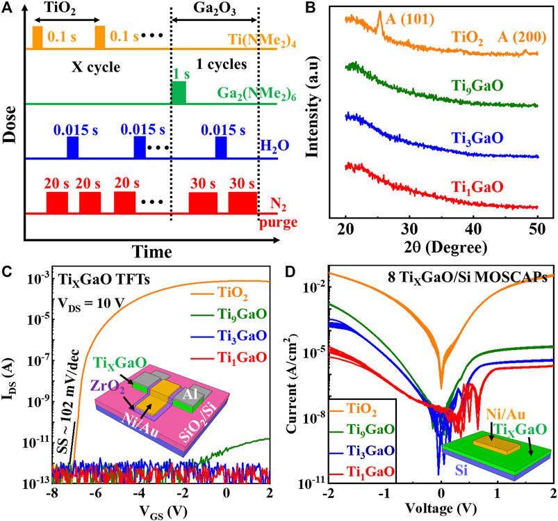
Figure 1. (A) Schematic of Ga-incorporated TiO2 thin films by atomic layer deposition, where the incorporated Ga level is controlled by cycle ratio (X) of TiO2 to that of Ga2O3. (B) Grazing incidence X-ray diffraction (GI-XRD) spectrum of 15 nm TiO2 and TiXGaO films after 500°C O2 annealing. (C) Transfer curves of thin film transistors (TFTs) under VDS of 10 V using 15 nm TiO2 and TiXGaO films as the channel materials. Inset: schematic of TiXGaO TFTs. (D) Leakage current density-voltage characteristic of TiO2/Si and TiXGaO/Si metal-oxide semiconductor capacitors (MOSCAPs). Inset: schematic of TiXGaO/Si MOSCAPs. Note that X represents the cycle ratio during ALD instead of atomic percentage for TiXGaO.
Figure 1B exhibits the grazing incidence X-ray diffraction (GI-XRD) spectrum of 15 nm TiO2 and TiXGaO films after 500°C O2 annealing. Distinct diffraction peaks at 25.4° and 48.2° can be observed for the TiO2 film, corresponding to the (101) and (200) facets of anatase TiO2, respectively (Zhang et al., 2019a). On the other hand, no observable peaks can be seen for TiXGaO films, indicating their amorphous nature. Thus, Ga could function as crystallization retarder to TiO2 host, destabilizing its crystallization under 500°C process. Figure 1C exhibits transfer curves of TFTs under VDS of 10 V using 15 nm TiO2 and TiXGaO films as the channel materials. The TiO2 TFTs show excellent switching behavior including a low SS of ∼102 mV/dec and a high Ion/Ioff of >109, being consistent with our previous work (Zhang et al., 2019a). On the other hand, the TiXGaO TFTs exhibit insignificant currents, which is also agree with the observation that the amorphous TiO2 film presents insulating properties in our previous study (Zhang et al., 2021a).
This can be explained by the structural disorder induced gap states of amorphized TiXGaO film preventing electrons from transport within the TiXGaO film (Zhang et al., 2021a; Zhang et al., 2021c). Figure 1D shows the current density-voltage (J-V) characteristic of TiO2/Si and TiXGaO/Si MOSCAPs, where the voltage is applied on top metal with Si substrate grounded. Consistent J-V behavior can be observed among 8 MOSCAPs for all the TiXGaO and TiO2 films, which suggests the high uniformity of ALD-derived films. The TiO2/Si MOSCAPs show a high leakage current with J value reaching 4.5 × 10⁻² A/cm-2 under −2 V bias and 3.5 × 10⁻² A/cm-2 under +2 V bias. The similarly large J values under both polarities of biases suggest that the TiO2 film could not provide sufficient barrier for both electrons and holes from Si to transport into TiO2 film by tunneling or field emission. The J values under both polarities of biases are decreased significantly upon Ga incorporation. Under −2 V bias, the J value decreases from 1.7 × 10⁻³ A/cm−2 to 2.1 × 10⁻⁴ A/cm−2 and 1.3 × 10⁻⁵ A/cm-2 for TiXGaO films when X reduces from 9 to 3 and 1, respectively. Similarly, under +2 V bias, the J value decreases from 1.9 × 10⁻⁵ A/cm-2 to 4.5 × 10⁻⁶ A/cm−2 and 2.4 × 10⁻⁶ A/cm−2 for TiXGaO films when X reduces from 9 to 3 and 1, respectively. The much-reduced J value under both bias voltages suggests that the increased barrier height for both electrons and holes from Si to transport into TiXGaO film by tunneling or field emission upon Ga incorporation. Additionally, the J values under +2 V bias are also lower than that of under −2 V bias, indicating that barrier height is larger for electrons compared to that of holes.
Figure 2A exhibits the capacitance-voltage (C-V) characteristics of TiO2/Si and TiXGaO/Si MOSCAPs at frequency of 1 kHz. It is interesting to find that no depletion region can be observed under positive bias voltage (Vbias) in C-V characteristic of TiO2/Si MOSCAPs, which agrees with the high J value under positive Vbias in Figure 1D. On the other hand, C-V characteristics of TiXGaO/Si MOSCAPs exhibit depletion regions, which can be explained by the low J value under positive Vbias after Ga incorporation. The maximum capacitances (CMAX) of these MOSCAPs are also marked in Figure 2A. Both Ti3GaO and Ti1GaO MOSCAPs reach CMAX under Vbias of −2 V, in contrast to that Ti9GaO and TiO2 MOSCAPs reach CMAX under Vbias of −1.44 V and −0.44 V, respectively. The sudden drop of capacitance of Ti9GaO and TiO2 MOSCAPs under more negative Vbias could be due to their high leakage currents (Bonkerud et al., 2021). The dielectric constant (k) value can be estimated according to:
where d is the thickness of TiO2 and TiXGaO films, and
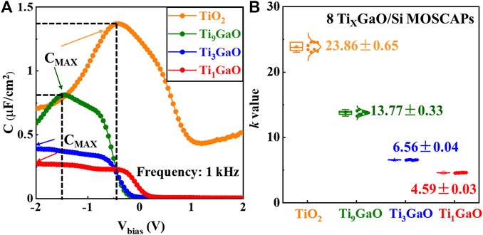
Figure 2. (A) Capacitance-voltage (C–V) characteristics of TiO2/Si and TiXGaO/Si MOSCAPs at frequency of 1 kHz, where the maximum capacitances (CMAX) of these MOSCAPs are marked. (B) Extracted dielectric constant (k) value of TiO2 and TiXGaO films from CMAX. Note that the k values of TiO2 and Ti9GaO can be underestimated due to the high leakage current.
X-ray photoelectron spectroscopy (XPS) measurements were conducted to uncover the modification of chemical states of TiO2 upon Ga incorporation, where spectra were taken from 15 nm TiO2/TiXGaO films on Si after 500°C O2 annealing. Figures 3A, B shows the Ti 2p and Ga 2p core-level spectrum, respectively. It is expected to observe that the intensity of Ti 2p spectrum is decreased whereas that of Ga 2p spectrum is increased with the decreased TiO2 to Ga2O3 cycle ratio X. The peak position of Ti spectrum is also shifted to a lower binding energy level upon Ga incorporation in Figure 3A, where a negative binding energy shift (∆E) of −0.17 eV can be observed from TiO2 to Ti1GaO. This is in contrast to that no distinct ∆E can be observed for Ga 2p spectrum in Figure 3B. Both Ti 2p and Ga 2p spectrum exhibit broadening features, where the full width at half maxima (FWHM) is increased from 0.81 eV for TiO2 to 1.27 eV for Ti1GaO in Figure 3A and that is increased from 1.28 eV for Ti9GaO to 1.43 eV for Ti1GaO in Figure 3B. The shifts and broadening features of spectrum could be due to the Ga substitution of Ti in TiO2 host, where a stronger Ti-O bond (776 kJ/mol) is replaced by Ga-O bond (374 kJ/mol) (Wang et al., 2018; To et al., 2023). Figure 3C shows the O 1s spectrum of TiO2 and TiXGaO films, where two peaks are fitted representing O bonding with metal cations (M-O) and O-related defects (VO) such as oxygen vacancy and hydroxyl. A positive ∆E of 0.45 eV can be observed in the M-O peaks from TiO2 to Ti1GaO, which is accompanied by an increase of 0.54 eV in FWHM accordingly. This can be also explained by the fact that Ga substitutes Ti, leading to more O atoms bonding with Ga atoms. It is interesting to note that the VO is increased upon Ga incorporation from 12% in TiO2 to 21% in Ti1GaO, suggesting that more O related-defects are introduced into the film due to the Ga incorporation. This is corroborated by the atomic percentage analysis of the film in Figure 3D, where the overall oxygen content is reduced from 66.6% in TiO2 to 59.5% in Ti1GaO. The reduced overall oxygen content and the increased O related-defects could be due to the fact that O/metal cation stoichiometry of TiO2 (value of 2) is higher than that of Ga2O3 (value of 1.5) and that the bonding energies of Ti-O bond (776 kJ/mol) is stronger than that of Ga-O bond (374 kJ/mol) (Wang et al., 2018; To et al., 2023). The VO is known to work as shallow donors and increase the electron concentration in oxides (Zhang et al., 2020; Zhang et al., 2023), which cannot explain the leakage current reduction in the MOSCAPs. It is also noted that the atomic percentage of Ga is much higher than the expected value from cycle ratio X. It might be due to the much longer pulse time of Ga precursor (1 s) compared to that of Ti precursor (0.1 s), and the different nucleation behaviors between Ti precursor on top of Ga-terminated surface and Ga precursor on top of Ti-terminated surface (Hong et al., 2021). The bandgap (Eg) of TiO2 and TiXGaO can be estimated from the O 1s plasmon energy loss feature in Figure 3E. It is found that the, Eg is increased upon Ga incorporation, the value of which is increased from 3.6 eV for TiO2 to 4.4 eV for Ti9GaO, 4.8 eV for Ti3GaO, and 5.2 eV for Ti1GaO. It needs to mention that the exact value of Eg should not be taken seriously due to the limits of extraction method, and it is the increasing trend that should be paid attention to. Figure 3F exhibits the valence band (VB) edge of TiO2 and TiXGaO films, where a downshift of valence band maximum (VBM) can be seen upon Ga incorporation. Overall, XPS results show that Ga incorporation induces more O-related defects, enlarges the Eg and slightly downshifts the VBM of TiO2.
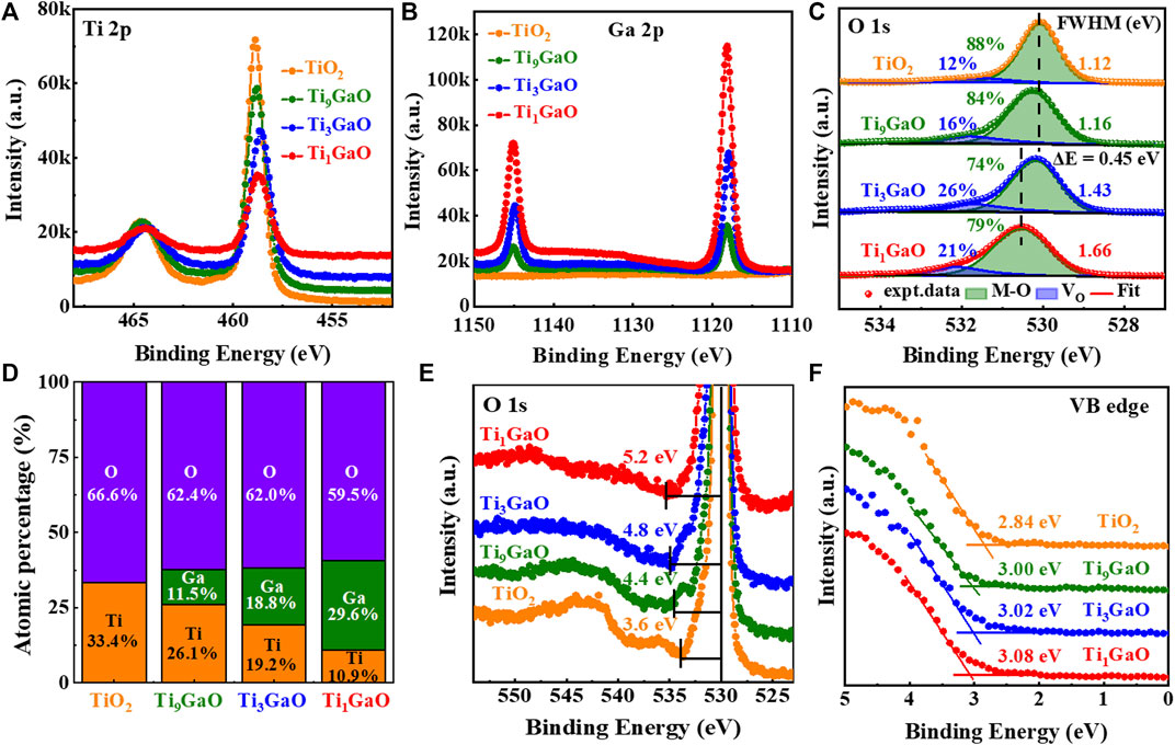
Figure 3. X-ray photoelectron spectroscopy (XPS) spectrum of (A) Ti 2p; (B) Ga 2p; and (C) O 1s of 500°C O2-annealed TiO2 and TiXGaO films with thickness of 15 nm. (D) Atomic percentage analysis of TiO2 and TiXGaO films. (E) O 1s plasmon energy loss for bandgap (Eg) extraction; and (F) valence band (VB) edge of TiO2 and TiXGaO films.
The surface morphologies of TiO2 and TiXGaO films were also examined by the atomic force microscope (AFM) in Figure 4. The AFM scans were in the tapping mode with the scan area of 1 × 1 μm2. All the films show a smooth surface with a low root mean square (RMS) roughness, the value of which are 0.51 nm for TiO2, 0.33 nm for Ti9GaO, 0.52 nm for Ti3GaO, and 0.45 nm for Ti1GaO, respectively. The low RMS value is crucial for suppressing surface-roughness-induced leakage current and reducing the surface-roughness-related interface traps, thus benefiting to their applications in electronic devices. The density of interface trap (Dit) between TiXGaO and Si were extracted by multi-frequency conductance (G/
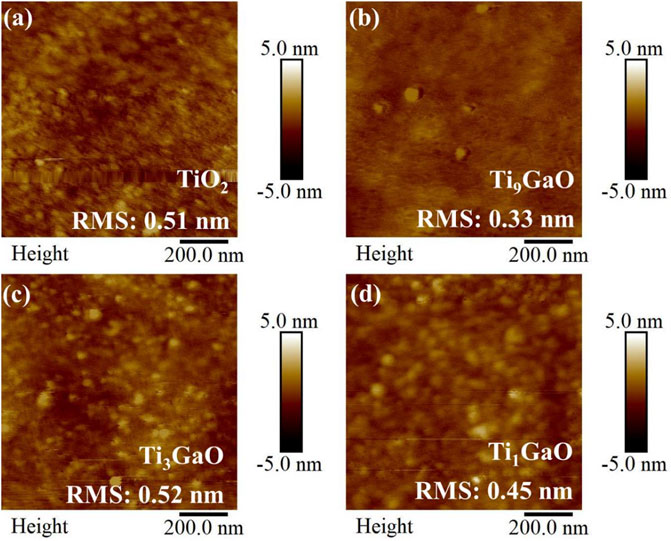
Figure 4. Atomic force microscope (AFM) scan of 15 nm (A) TiO2; (B) Ti9GaO; (C) Ti3GaO; and (D) Ti1GaO films on Si substrate after 500°C O2 annealing, exhibiting a smooth surface with low root mean square (RMS) roughness. The scan area is 1 × 1 μm2.
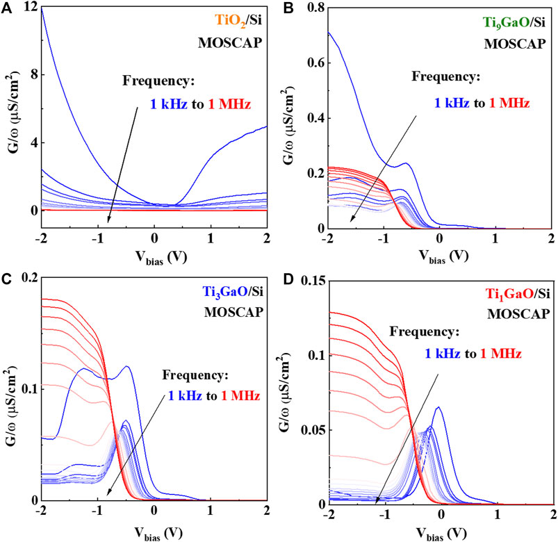
Figure 5. Multi-frequency conductance-voltage (G–V) measurement of (A) TiO2/Si; (B) Ti9GaO/Si; (C) Ti3GaO/Si; and (D) Ti1GaO/Si MOSCAPs, where the applied frequency is varied from 1 kHz to 1 MHz.
The behavior of equivalent parallel conductance (G/ω) as a function of angular frequency (ω) can be modelled by the equation (Liu et al., 2015; Chandrasekar et al., 2017):
where e is the elementary electron charge, Dit is the density of interface trap,
where
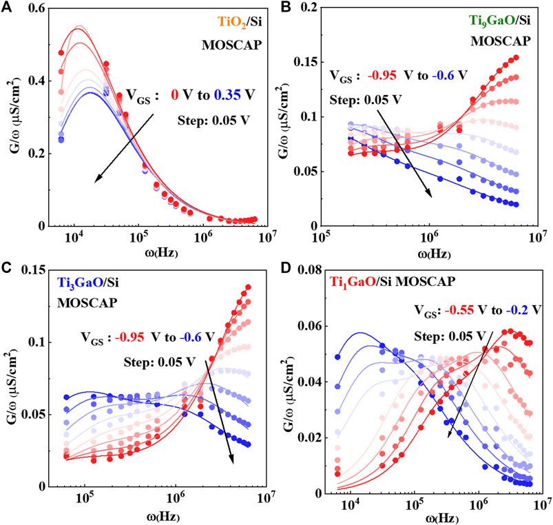
Figure 6. Equivalent parallel conductance (G/
Figure 7A exhibits the extracted Dit as a function of the EC-ET for TiO2/Si and TixGaO/Si MOSCAPs based on Eqs 2, 3. A “U-shape” profile of interface trap can be observed for all the MOSCAPs, with a similar level of Dit values ranging from 4 × 10¹¹ eV−1cm−2 to 1013 eV−1cm−2. This similar level of Dit can be originated from the growth schematic of our TiXGaO films, which starts with TiO2 growth cycle and may result in similar interface quality between TiXGaO and Si. Thus, the reduced leakage current in TixGaO/Si MOSCAPs with increased Ga incorporation could not be explained by interface trap passivation, which is also corroborated by XPS results showing increased O-related defects by Ga incorporation. Figure 7B shows the band alignment of Si, TiO2, and Ti1GaO derived from XPS results (Figure 3), where the valence band (EV) offset is increased by 0.24 eV and the conduction band (EC) offset is increased by 1.36 eV with Ga incorporation. The increased band offset can function as potential barrier for carriers, thereby reducing the leakage current. The asymmetric band offset could also explain why leakage currents of TixGaO/Si MOSCAPs are lower under positive Vbias than that of under negative Vbias in Figure 1D, where electrons are more difficult to overcome the larger EC offset. Base on the above information, it is believed that the reduction of the leakage current in TixGaO/Si MOSCAPs upon Ga incorporation could be explained by the amorphization of TiXGaO film and the enlarged band-offset to Si rather than defect passivation.
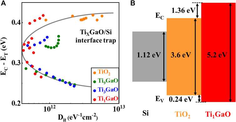
Figure 7. (A) Extracted Dit as a function of the trap energy level relative to the conduction band of Si (EC-ET) for TiO2/Si and TixGaO/Si MOSCAPs. A “U-shape” profile of interface trap can be observed and the differences of Dit values between TixGaO/Si MOSCAPs are not pronounced. (B) Band alignment of Si, TiO2, and Ti1GaO, where the leakage current reduction could be due to the amorphization of TiO2 and the enlarged band-offset upon Ga incorporation.
3 Conclusion
In summary, we demonstrate that the Ga incorporation could be an effective way to improve the dielectric performances of TiO2 films. Pure TiO2 thin films could be the channel material for TFT application whereas Ga-incorporated TiO2 thin films could be used as high-k dielectric with good insulating properties. The leakage current and k value are decreased with the increased Ga content, while the Dit value between TiXGaO and Si maintain roughly at the same level. The reduction of leakage current upon Ga incorporation is believed to be due to that the amorphization of TiO2 and enlarged band offset to Si rather than oxygen defect passivation. These Ga-incorporated TiO2 films with well-behaved dielectric property under a process temperature of 500 °C may found promising usage in future electronic devices such as trench capacitors in DRAM.
Data availability statement
The raw data supporting the conclusion of this article will be made available by the authors, without undue reservation.
Author contributions
QS: Formal Analysis, Writing–original draft. YnL: Formal Analysis, Validation, Writing–original draft. CH: Data curation, Writing–review and editing. ZY: Data curation, Validation, Writing–review and editing. YgL: Data curation, Validation, Writing–review and editing. YZ: Project administration, Supervision, Writing–review and editing. WY: Project administration, Supervision, Writing–review and editing. JZ: Funding acquisition, Project administration, Writing–original draft, Writing–review and editing.
Funding
The author(s) declare that financial support was received for the research, authorship, and/or publication of this article. This work was supported by the Central University Basic Research Fund of China under Grant No. 20720230040, Fujian Minjiang Distinguished Scholar Program, Xiamen Double-Hundred-Talent Program, and the National Natural Science Foundation of China under Grant No. 62171396.
Conflict of interest
The authors declare that the research was conducted in the absence of any commercial or financial relationships that could be construed as a potential conflict of interest.
Publisher’s note
All claims expressed in this article are solely those of the authors and do not necessarily represent those of their affiliated organizations, or those of the publisher, the editors and the reviewers. Any product that may be evaluated in this article, or claim that may be made by its manufacturer, is not guaranteed or endorsed by the publisher.
References
Bonkerud, J., Zimmermann, C., Weiser, P. M., Vines, L., and Monakhov, E. V. (2021). On the permittivity of titanium dioxide. Sci. Rep. 11 (1), 12443. doi:10.1038/s41598-021-92021-5
Campbell, S., Kim, H., Gilmer, D., He, B., Ma, T., and Gladfelter, W. (1999). Titanium dioxide (TiO2)-based gate insulators. Ibm J. Res. Dev. 43 (3), 383–392. doi:10.1147/rd.433.0383
Chandrasekar, H., Bhat, K. N., Rangarajan, M., Raghavan, S., and Bhat, N. (2017). Thickness dependent parasitic channel formation at AlN/Si interfaces. Sci. Rep. 7, 15749. doi:10.1038/s41598-017-16114-w
Charnas, A., Zhang, Z., Lin, Z., Zheng, D., Zhang, J., Si, M., et al. (2023). Review-extremely thin amorphous indium oxide transistors. Adv. Mater. 36, e2304044. doi:10.1002/adma.202304044
Datta, S., Dutta, S., Grisafe, B., Smith, J., Srinivasa, S., and Ye, H. (2019). Back-End-of-Line compatible transistors for monolithic 3-D integration. IEEE Micro 39 (6), 8–15. doi:10.1109/MM.2019.2942978
Han, K., Kong, Q., Kang, Y., Sun, C., Wang, C., Zhang, J., et al. (2021). “First demonstration of oxide semiconductor nanowire transistors: a novel digital etch technique, igzo channel, nanowire width down to 20 nm, and Ion exceeding 1300 μA/μm,” in 2021 Symposium on VLSI Technology, Kyoto, Japan, 13-19 June 2021, 1–2.
Hong, T., Jeong, H.-J., Lee, H.-M., Choi, S.-H., Lim, J. H., and Park, J.-S. (2021). Significance of pairing in/Ga precursor structures on PEALD InGaOx thin-film transistor. ACS Appl. Mater. Inter 13 (24), 28493–28502. doi:10.1021/acsami.1c06575
Katayama, M., Ikesaka, S., Kuwano, J., Koinuma, H., and Matsumoto, Y. (2008). High quality anatase TiO2 film: field-effect transistor based on anatase TiO2. Appl. Phys. Lett. 92 (13). doi:10.1063/1.2906361
Kim, S. K., Kim, K. M., Jeong, D. S., Jeon, W., Yoon, K. J., and Hwang, C. S. (2013). Titanium dioxide thin films for next-generation memory devices. J. Mater. Res. 28 (3), 313–325. doi:10.1557/jmr.2012.231
Kim, T., Choi, C. H., Hur, J. S., Ha, D., Kuh, B. J., Kim, Y., et al. (2023). Progress, challenges, and opportunities in oxide semiconductor devices: a key building block for applications ranging from display backplanes to 3D integrated semiconductor chips. Adv. Mater. 35 (43), e2204663. doi:10.1002/adma.202204663
Liao, P.-Y., Khot, K., Alajlouni, S., Snure, M., Noh, J., Si, M., et al. (2023). Alleviation of self-heating effect in top-gated ultrathin In2O3 FETs using a thermal adhesion layer. IEEE Trans. Electron Devices 70 (1), 113–120. doi:10.1109/TED.2022.3221358
Liu, S., Yang, S., Tang, Z., Jiang, Q., Liu, C., Wang, M., et al. (2015). Interface/border trap characterization of Al2O3/AlN/GaN metal-oxide-semiconductor structures with an AlN interfacial layer. Appl. Phys. Lett. 106 (5). doi:10.1063/1.4907861
Park, J.-W., Han, S.-W., Jeon, N., Jang, J., and Yoo, S. (2008). Improved electrical characteristics of amorphous oxide TFTs based on TiOx channel layer grown by low-temperature MOCVD. IEEE Electron Device Lett. 29 (12), 1319–1321. doi:10.1109/LED.2008.2005737
Park, J.-W., Lee, D., Kwon, H., Yoo, S., and Huh, J. (2009). Performance improvement of N-type TiOx active-channel TFTs grown by low-temperature plasma-enhanced ALD. IEEE Electron Device Lett. 30 (7), 739–741. doi:10.1109/LED.2009.2021587
Park, J. Y. (2018). How titanium dioxide cleans itself. Science 361 (6404), 753. doi:10.1126/science.aau6016
Samanta, S., Han, K., Sun, C., Wang, C., Thean, A. V.-Y., and Gong, X. (2020). “Amorphous IGZO TFTs featuring extremely-scaled channel thickness and 38 nm channel length: achieving record high Gm,max of 125 μS/μm at VDS of 1 V and ION of 350 μA/μm,” in 2020 Symposium on VLSI Technology, Honolulu, HI, USA, 16-19 June 2020, 1–2. doi:10.1109/vlsitechnology18217.2020.9265052
Si, M., Lin, Z., Chen, Z., Sun, X., Wang, H., and Ye, P. D. (2022). Scaled indium oxide transistors fabricated using atomic layer deposition. Nat. Electron. 5 (3), 164–170. doi:10.1038/s41928-022-00718-w
Sze, S. M., and Ng, K. K. (2006). “Physics and properties of semiconductors—a review,” in Physics of semiconductor devices (John Wiley and Sons, Ltd), 5–75. doi:10.1002/9780470068328.ch1
To, T., Olsen, A. A. K. R. K., Hansen, B. A., Enevoldsen, K. M., Lutken, V., Jensen, L. R., et al. (2023). Comparing the effects of Ga2O3 and Al2O3 on the structure and mechanical properties of sodium borate glasses. J. Non-Cryst Solids 618, 122506. doi:10.1016/j.jnoncrysol.2023.122506
Wang, B., Huang, W., Chi, L., Al-Hashimi, M., Marks, T. J., and Facchetti, A. (2018a). High-k gate dielectrics for emerging flexible and stretchable electronics. Chem. Rev. 118 (11), 5690–5754. doi:10.1021/acs.chemrev.8b00045
Wang, L., Chen, B., Ma, J., Cui, G., and Chen, L. (2018b). Reviving lithium cobalt oxide-based lithium secondary batteries-toward a higher energy density. Chem. Soc. Rev. 47 (17), 6505–6602. doi:10.1039/C8CS00322J
Wilk, G., Wallace, R., and Anthony, J. (2001). High-κ gate dielectrics: current status and materials properties considerations. J. Appl. Phys. 89 (10), 5243–5275. doi:10.1063/1.1361065
Zhang, J., Charnas, A., Lin, Z., Zheng, D., Zhang, Z., Liao, P.-Y., et al. (2022). Fluorine-passivated In2O3 thin film transistors with improved electrical performance via low-temperature CF4/N2O plasma. Appl. Phys. Lett. 121 (17). doi:10.1063/5.0113015
Zhang, J., Cui, P., Lin, G., Zhang, Y., Sales, M. G., Jia, M., et al. (2019b). High performance anatase-TiO2 thin film transistors with a two-step oxidized TiO2 channel and plasma enhanced atomic layer-deposited ZrO2 gate dielectric. Appl. Phys. Express. 12 (9), 096502. doi:10.7567/1882-0786/ab3690
Zhang, J., Jia, M., Sales, M. G., Zhao, Y., Lin, G., Cui, P., et al. (2021b). Impact of ZrO2 dielectrics thickness on electrical performance of TiO2 thin film transistors with sub-2 V operation. ACS Appl. Mater. Inter. 3 (12), 5483–5495. doi:10.1021/acsaelm.1c00909
Zhang, J., Lin, G., Cui, P., Jia, M., Li, Z., Gundlach, L., et al. (2020). Enhancement-/Depletion-Mode TiO2 thin-film transistors via O2/N2 preannealing. IEEE Trans. Electron. Devices 67 (6), 2346–2351. doi:10.1109/TED.2020.2988861
Zhang, J., Sales, M. G., Lin, G., Cui, P., Pepin, P., Vohs, J. M., et al. (2019a). Ultrathin-body TiO2 thin film transistors with record on-current density, ON/OFF curren ratio, and subthreshold swing via O2 annealing. IEEE Electron Device Lett. 40 (9), 1463–1466. doi:10.1109/LED.2019.2927571
Zhang, J., Wei, L., Jia, M., Cui, P., and Zeng, Y. (2021c). “Crystallinity engineering of stoichiometric TiO2: transition from insulator to semiconductor,” in 2021 Device Research Conference (DRC), Santa Barbara, CA, USA, 20-23 June 2021, 1–2. doi:10.1109/drc52342.2021.9467219
Zhang, J., Zhang, Y., Cui, P., Lin, G., Ni, C., and Zeng, Y. (2021a). One-volt TiO2 thin film transistors with low-temperature process. IEEE Electron Device Lett. 42 (4), 521–524. doi:10.1109/LED.2021.3060973
Zhang, J., Zheng, D., Zhang, Z., Charnas, A., Lin, Z., and Ye, P. D. D. (2023). Ultrathin InGaO thin film transistors by atomic layer deposition. IEEE Electron Device Lett. 44 (2), 273–276. doi:10.1109/LED.2022.3233080
Zheng, D., Charnas, A., Anderson, J., Dou, H., Hu, Z., Lin, Z., et al. (2022). First demonstration of BEOL-compatible ultrathin atomiclayer-deposited InZnO transistors with GHz operation and record high bias-stress stability. IEDM Tech. Dig. Dec. 2022, 1–4. doi:10.1109/IEDM45625.2022.10019452
Keywords: Ga incorporation, atomic layer deposition, crystallinity, high-permittivity dielectric, band alignment, interface traps, thin film transistor, dynamic random-access memory
Citation: Sun Q, Lin Y, Han C, Yang Z, Li Y, Zeng Y, Yang W and Zhang J (2024) Gallium-incorporated TiO2 thin films by atomic layer deposition for future electronic devices. Front. Mater. 11:1430884. doi: 10.3389/fmats.2024.1430884
Received: 10 May 2024; Accepted: 23 May 2024;
Published: 13 June 2024.
Edited by:
Dongqi Zheng, Apple Inc., United StatesReviewed by:
Sunbin Deng, Georgia Institute of Technology, United StatesYaoqiao Hu, The University of Texas at Dallas, United States
Copyright © 2024 Sun, Lin, Han, Yang, Li, Zeng, Yang and Zhang. This is an open-access article distributed under the terms of the Creative Commons Attribution License (CC BY). The use, distribution or reproduction in other forums is permitted, provided the original author(s) and the copyright owner(s) are credited and that the original publication in this journal is cited, in accordance with accepted academic practice. No use, distribution or reproduction is permitted which does not comply with these terms.
*Correspondence: Jie Zhang, jayzhang@xmu.edu.cn
†These authors have contributed equally to this work