 David B. Go1,2*
 John R. Haase1,2
 Jeffrey George3Jochen Mannhart4
 Robin Wanke4Alireza Nojeh5Robert Nemanich6
- 1Department of Aerospace and Mechanical Engineering, University of Notre Dame, Notre Dame, IN, United States
- 2Department of Chemical and Biomolecular Engineering, University of Notre Dame, Notre Dame, IN, United States
- 3Johnson Space Center, National Aeronautics and Space Administration (NASA), Houston, TX, United States
- 4Max Planck Institute for Solid State Research, Stuttgart, Germany
- 5Department of Electrical and Computer Engineering, Quantum Matter Institute, University of British Columbia, Vancouver, BC, Canada
- 6Department of Physics, Arizona State University, Tempe, AZ, United States
Thermionic energy conversion (TEC) is the direct conversion of heat into electricity by the mechanism of thermionic emission, the spontaneous ejection of hot electrons from a surface. Although the physical mechanism has been known for over a century, it has yet to be consistently realized in a manner practical for large-scale deployment. This perspective article provides an assessment of the potential of TEC systems for space and terrestrial applications in the twenty-first century, overviewing recent advances in the field and identifying key research challenges. Recent developments as well as persisting research needs in materials, device design, fundamental understanding, and testing and validation are discussed.
Introduction
The direct conversion of heat to electricity without any intermediate steps or moving parts remains one of the most promising, yet challenging, methods of power production. The promise of high conversion efficiency, device simplicity, and robust operation continues to push research and technology development at the cutting edge. Furthermore, because of the wide variety of possible heat sources, ranging from combustion of fossil or other fuels, nuclear reactors, solar heat, or even waste heat from the human body, the applications for thermal-to-electric energy convertors are vast, spanning many orders of magnitude of possible temperature and power ranges.
Thermionic energy conversion (TEC) for direct conversion of heat to electrical energy occurs when electrons thermally emit from a hot surface, traverse a gap, and are collected by another surface. This process, starting with thermionic emission, produces a current of electrons that can subsequently drive an electrical load to produce work. Particularly well suited for high-temperature applications, since it was first proposed by Schlichter (1915), thermionic emission has been pursued as a power generation method for over a century (Hatsopoulos and Gyftopoulos, 1973, 1979), yet has seldom been realized in either space or terrestrial applications. However, recent advances in material science and nanotechnology as well as our evolving understanding of the underlying physical processes afford new opportunities to develop practical thermionic convertors, reinvigorating the field.
Thermionic energy conversion has a long and storied history, particularly in the space programs of the United States and the former Soviet Union. However, while the field was vibrant and much progress was made during the 1960s through 1980s, including space flight demonstrations, TEC has largely been supplanted by alternative energy conversion technologies, specifically thermoelectrics and photovoltaics, in both the public and research community consciences. Much of thermionic-based research tapered off after a 2001 report by the National Research Council titled Thermionics Quo Vadis? An Assessment of the DTRA’s Advanced Thermionics Research and Development Program (National Research Council, 2001) provided a fairly negative perspective on the viability of TEC. However, since that time the TEC research community has responded by discovering and inventing new and novel approaches to devices, materials, and operating strategies that highlight the potential of TEC to achieve the high conversion efficiency and performance predicted by theory.
As both space and terrestrial energy needs continue to grow, it is not only compelling but necessary to develop new technologies for power generation. For space applications, new missions, including to Mars, and new technologies, such as miniature satellites (e.g., CubeSats), will require power sources that deliver high power in reliable and sustained ways over long periods of time. From the terrestrial perspective, there is an ongoing need to find alternative energy sources as well as improve the efficiency of existing fossil fuel-driven power sources, especially with growing concerns about the environmental and climate impact of traditional coal and oil-fired power plants, environmental and economic challenges facing fossil fuel extraction, and the ongoing challenge of fossil fuel depletion.
In October, 2014, a Workshop on Thermionic Energy Conversion for Space and Earth was held in Houston, TX (United States) to bring together researchers, thought leaders, and stake holders to discuss the current state of TEC and opportunities and needs for future research and development to address the challenges. Perhaps more importantly, the Workshop served to centralize and collect the TEC community, and bring together somewhat independent and isolated researchers to a common table to discuss and promote this important energy technology. This perspective article is a result of this workshop and ensuing discussions among the participants. The purpose of this article is not only to discuss recent advances but also to offer some perspectives on the field in terms of possibilities as well as challenges, from the collective wisdom of the workshop participants. We do note that it is not the intent of the article to provide a detailed review of recent research, and for that we point the reader to other recent review articles (Khoshaman et al., 2014; McCarthy et al., 2014; Khalid et al., 2016; Trucchi and Melosh, 2017).
This perspective article is organized into several sections as follows. “Background and Fundamentals” gives background on thermionic emission and TEC, including establishing the fundamentals of TEC and the terminology that will be used throughout this article as well as opportunities for TEC implementation. “Challenges and Recent Advances” outlines recent advances in TEC research, focusing on the primary components of a TEC device—the emitter, the electrode gap, and the collector. “Going Forward” discusses future research needs, focusing primarily on the need to establish a set of guidelines for testing and evaluating TEC devices. We conclude with “Summary and Final Thoughts,” which offers some perspectives and suggestions for a path forward.
Background and Fundamentals
Fundamental Physics of TEC
The basic concept of TEC is outlined in Figure 1A. As heat is added to the emitter (cathode) and the emitter temperature rises, electrons have sufficient energy to escape the solid and move freely in the vacuum, a process likened to evaporation or boiling off of electrons. These electrons then move across an electrode gap to a collector (anode), and completing the circuit with a load produces electrical power. Figure 1B shows this process of thermionic emission from the perspective of the energy levels of the electrons. To be emitted, electrons in the emitter must be energized to be above the vacuum potential barrier of the emitter, where the difference between the vacuum potential and the Fermi energy is called the work function (ϕ). If no collisional or space-charge effects limit the electron transport through the interelectrode gap, the electrons traverse the gap and enter the collector, where the ideal output voltage (Vout) is approximately the contact potential difference.
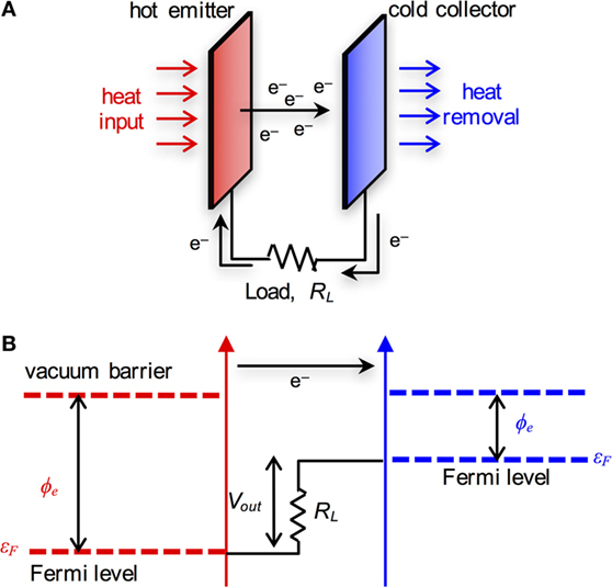
Figure 1. (A) Schematic of the thermionic energy conversion (TEC) process. (B) Electromotive diagram showing electron energy levels during TEC.
Thermionic emission is described by the Richardson–Dushman equation (Richardson, 1921), which relates thermionic current density (j) to the temperature of the emitter (Te) as follows:
where A0 = 120 A/cm2 K2 is the Richardson constant and kB is the Boltzmann constant. The parameter A is a correction factor to the Richardson constant for a specific emitter material. If an electric field (E) is applied between the emitter and the collector, the potential barrier is lowered. The resulting emission current is described by the Schottky equation (Schottky, 1914):
where q is the electron charge and ε0 is the permittivity of free space.
From the electromotive diagram in Figure 1B, we see that the maximum voltage (at maximum power) that can be achieved is essentially the difference between the work functions of the emitter and collector,
Given that the power density P is given by
the efficiency (η) is the power density produced by the thermionic convertor divided by the net heat flux supplied to the emitter , which includes heat losses due to electron emission, conduction down the leads and other paths, and heat exchange (predominantly radiation) from the hot emitter to the collector,
From these equations, it becomes clear that there are a number of factors that directly influence the amount of power produced by a thermionic convertor, as well as its efficiency, that are often in direct competition with each other. From Eq. 1 (and Figure 1B), we see that the current density increases when the emitter work function is small. However, to generate high power, large work function differences between the emitter and collector are needed, and thus the work function of the collector must be even smaller than that of the emitter, which is a significant materials challenge. Practically, the collector work function should be ~0.5 eV, which is extremely small compared with the work function of most natural materials. In addition, to generate sufficient current for conventional emitter materials, the temperature of the emitter must be very high and typically much greater than 1,500 K. However, this leads to greater thermal losses due to both radiation and conduction, decreasing the efficiency of the thermionic convertor. There are also additional fundamental challenges in TEC that do not appear directly in these equations, and prime among these is the space-charge effect. At sufficiently high current density, electrons build-up in the interstitial gap between the electrodes and create a space-charge barrier that limits the current to that described by the Child–Langmuir law (Child, 1911; Langmuir, 1913), as opposed to the Richardson–Dushman equation. Hence, managing the electron transport across the electrode gap is also an essential aspect of TEC design.
History of TEC
The first thermionic conversion device was proposed by Schlichter in 1915 (Schlichter, 1915), but the first demonstrations of practical levels of power generation were not made until the 1950s when both the United States and the former Soviet Union (USSR), as well as Western European nations, began exploring TEC for space applications in earnest (Rasor, 1991). Early United States developments aimed for solar energy and radioisotopes as thermal sources, and the Jet Propulsion Laboratory Solar Energy Technology program developed thermionic convertors that operated at ~1,900 K and ~150 W with 7–11% efficiency for up to ~11,000 h. However, the state-of-the-art at the time proved uncompetitive with emerging photovoltaic and thermoelectric energy conversion strategies, and the program was discontinued in the 1970s. In the 1960s, the focus shifted to nuclear heat sources and the development of both in-core and out-of-core thermionic converters with cesium (Cs) plasma often introduced to overcome space-charge limitations. While the United States made significant progress in improving thermionic nuclear fuel element (TFE) performance leading to the Mark III reactor that operated at 1,900 K for nearly 12,500 h, the thermionic reactor development program was ultimately canceled in 1973. In the 1970s, the focus shifted to terrestrial fossil fuel thermal sources, but with middling success and there were no major developments. There was renewed interest in TFEs in the 1980s through the SP-100 program in a joint effort between NASA, the Department of Energy, and the Department of Defense. The Thermionic Fuel Element Verification program produced a number of analyses that suggested that a 3- to 7-year lifetime was possible, but no major reactors were demonstrated. The USSR primarily focused on developing full-scale thermionic reactors and in 1970 developed the 5 kW TOPAZ reactor (a Russian acronym for Thermionic Experiment with Conversion in Active Zone) (Benke, 1994; Gryaznov, 2000), with a 6 kW version flying on a naval reconnaissance satellite in 1987 being one of two units that were ultimately flown. During this time, their more focused research effort also led to major advances in materials and convertor design, outstripping many of the United States advances (National Research Council, 2001).
Viability of TEC
Despite the aforementioned space charge and materials (work function) challenges and the tapering off in research, TEC still remains an attractive approach to power generation. Like other direct energy conversion approaches, it requires no moving parts and thus has the potential for long lifetimes with little-to-no maintenance. Further, it can generate high power but typically only requires small volumes and is lightweight, and thus its high specific power makes it particularly attractive to space applications.
Thermionic power convertors are the simplest and most straightforward convertors of heat into electric power, which is the fundamental reason why the conversion process runs rather close to thermodynamic equilibrium (Fitzpatrick et al., 1997). Entropy production is kept small, because unnecessary processes that would add to entropy production are avoided. Like all heat engines, the energy conversion efficiency is absolutely limited by the Carnot efficiency, but there are few other inherent limitations to efficient energy generation, with the predominant loss being thermal losses. Thus, at least ideally, it is possible for a thermionic convertor to approach the Carnot efficiency. Further, given the high temperatures thermionic emission is compatible with, this efficiency can be relatively high. For example, a “standard” convertor might operate with an 1,800 K emitter and 1,000 K collector, leading to Carnot efficiency of 44%. When compared with other technologies, such as thermoelectric convertors, the ability to operate at high temperatures is particularly attractive for high-power generation. Ultimately, while there are practical challenges to realizing efficient and effective thermionic convertors, they are not inherently limited by any physical or chemical means. That is, there is no physical/chemical reason that a thermionic converter cannot operate near the Carnot efficiency with high-power generation. It is compelling, therefore, to continue to pursue the development of TEC technologies.
Adding to the attractiveness of thermionic energy converters is that they can be combined with other technologies to extract otherwise unused thermal energy, and this is an interesting path forward. These waste heat harvesting strategies can be sorted into three categories: cogeneration, topping cycles, and replacement devices. Cogeneration is using an existing untapped heat source, such as waste heat from a combustor used in an industrial setting, to generate electricity without significantly affecting the process. Fitzpatrick et al. (1997) recommend a cogeneration process in which the collector is cooled by the gases entering the combustor, simultaneously preheating it, and after combustion, the waste gas is passed over the emitter, producing the temperature difference. Thermionic converters can also be used in topping cycles by placing the converter between a high-temperature source and a system used to generate energy requiring a lower input temperature (bottom cycle), with examples of possible bottom cycles including steam turbine Rankine cycles in power stations and Sterling cycles for solar energy (Fitzpatrick et al., 1997). With the development of photon-enhanced thermionic emission or PETE (Schwede et al., 2010) as discussed in Section “Emission,” combining solar concentrator systems with photon-enhanced thermionic converters as a topping cycle has the opportunity to produce highly efficient systems (Voesch et al., 2017). However, if the complexity, cost, or weight prohibit the use of multiple systems, then thermionic energy converters may be directly used for solar thermal-to-electrical energy conversion due to their higher possible efficiency. The United States Air Force Research Laboratory’s experimental High-Power Advanced Low Mass, for example, explored substituting concentrated-solar thermionic converters for photovoltaics (Adams, 2006). These various use cases highlight the possible gains of incorporating thermionic energy converters into the power generation ecosystem, reducing wasted energy, and increasing the efficiency of generation systems.
Challenges and Recent Advances
As noted in Section “Background and Fundamentals,” there are two primary issues and challenges that face all thermionic energy converters. First, as shown in Eq. 3, the output voltage, and with it the output power, of a thermionic convertor scales with the difference between the work functions of the emitter and the collector. As the emitter work function needs to be small enough to provide a large emission current at operation temperature, this requires the collector work function to be even lower and as small as possible, pushing the limits of materials. Second, space charge that inherently limits the emitter–collector current is a very real challenge that must be addressed for any TEC device to achieve practical power outputs. Additional challenges exist for specific applications, such as the ability to efficiently heat the cathode using sunlight in solar thermionics. To address these challenges requires advancing the technology of all the components of a thermionic heat engine: the emitter, the electrode gap architecture, and the collector. In this section, we discuss challenges and advances for each of these components, outlining some of the basic design requirements for being successful, historical and recent developments in addressing these requirements, and future needs.
Emission
Requirements
The emitter is the source of electrons in a TEC system, and as shown in Eq. 1, thermionic emission follows the Richardson–Dushman relation. The work function, ϕ, and the Richardson (or emission) constant, A, are materials-related parameters that determine the electron emission current density. The work function is typically described as the energy barrier between the Fermi level of a metal and the vacuum level for an electron at rest to be separated from the surface. For metals, the work function is well defined and fairly well known, and measurements by photoemission or the photoelectric effect typically agree well with the value deduced from a Richardson–Dushman analysis of the thermionic emission current density (Fomenko, 1966). Semiconducting materials have also recently been considered for low work function thermionic emitters. For semiconductors, the Fermi level can be controlled by dopant impurities. Moreover, band bending due to surface states can substantially impact the position of the Fermi level at the surface. Consequently, the work function for a specific semiconductor does not have a single value but a range of values that depends on the doping, the surface states, and the temperature. However, the electron affinity, which relates the position of the vacuum level to the conduction band minimum, is typically independent of doping and band bending and can be used to describe the surface barrier for electron emission (Schwede et al., 2010).
While an appropriate surface termination lowers the work function of metallic surfaces (Jenkins, 1969), for a semiconductor, an appropriate surface termination lowers the electron affinity or position of the vacuum level relative to the conduction band minimum (Jenkins, 1969). In some cases, the vacuum level can be positioned below the conduction band minimum resulting in a negative electron affinity (NEA). For a semiconductor with a NEA, the electron emission is presumed to originate from the conduction band minimum and the Richardson–Dushman barrier would be between the Fermi level and the conduction band minimum, although other emission processes may also occur. The presence of a NEA on either the emitter or collector results in a lowering of the space-charge barrier. This effect is understandable, as electrons emitted from the conduction band of the semiconductor would have a kinetic energy equal to or greater than the value of the NEA, which enables them to surmount an equivalent energy barrier.
In addition to requirements on the work function, there are additional aspects that must be considered. These include the robustness and stability of the material and/or surface termination at high temperatures, high current capacity, and high voltage capability, and the thermal properties of the material. For example, thermal radiation is a loss process in TEC that lowers the overall efficiency, and thus preparing a surface with a low emissivity can enhance the system efficiency. We summarize these various requirements in Table 1, which focuses only on the emitter. Note that these may also affect other aspects of a TEC device, such as a low work function emitter implicitly placing a requirement on the work function of the collector.
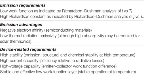
Table 1. Emitter requirements and advantages, and device-related requirements.
Current State-of-the-Art and Recent Advances
As the emitter plays a crucial role in TEC operation, a significant amount of research effort has focused on developing appropriate emission materials. As such, a wide range of materials is now being considered for thermionic emission and TEC systems. Some of these are summarized below.
Refractory Metals with Cs
Refractory metals continue to be the material of choice for high-temperature TEC emitters. Research has shown the advantage for single crystal surfaces of refractory metals including niobium, rhenium, tungsten, and molybdenum and alloys (Fomenko, 1966; Baksht et al., 1978). Advances in chemical vapor deposition have enabled non-planar configurations (Macdonald et al., 1989). These surfaces are typically employed in a TEC with an ignited Cs plasma, as the Cs adsorbed on the emitter surface reduces the work function to values of ~1.5 eV (Wilson, 1959; Aamodt et al., 1962; Norris, 1964).
Scandates and Barium (Ba) Dispenser Emitters
Early studies established that free Ba reduced the work function of oxide surfaces and various combinations of Ba–Sr–Ca oxides led to lower work functions (Jenkins, 1969). These materials were incorporated into emitters with metallic support to enhance electrical supply through the high resistivity oxides. Typical emitters are formed from porous tungsten impregnated with Ba–Sr–Ca oxides (Jenkins, 1969; Gibson et al., 1989). At high temperature, the Ba evaporates and must be replaced, which limits the lifetime of the sources. The inclusion of a scandium oxide (Sc2O3) layer on the surface of the impregnated emitter provides a substantial enhancement of the emission current density, which has been attributed to a lower work function. While Ba is a necessary component of scandate emitters, the details of the surface structure are still under study.
Diamond and Wide-Bandgap Semiconductors
The wide-bandgap semiconductors of diamond, boron nitride (BN), and aluminum nitride (AlN) have high melting temperatures, have shown negative or small electron affinities, and have been considered for electron emission applications (Nemanich et al., 1996; Sugino et al., 2002). For single crystal diamond, it has been established that hydrogen-terminated surfaces display a NEA, and n-type character is obtained through doping with nitrogen or phosphorus (Figure 2) (van der Weide et al., 1994; Diederich et al., 1998; Kataoka et al., 2010). Nitrogen- and phosphorus-doped diamond exhibit deep donor levels at ~1.7 and 0.6 eV, respectively. Thermionic emission from nitrogen-doped, single crystal diamond surfaces and polycrystalline diamond films indicated work functions of ~2.0 and ~1.4 eV, respectively (Koeck et al., 2009; Nemanich et al., 2010). The higher work function from the single crystal surface was attributed to band bending effects. The surfaces exhibit lower than expected current densities, which may be attributed to the material’s resistivity and/or the Richardson constant. Emission instabilities may be related to hydrogen desorption. Notably, similar results have been reported by several groups (Ristein, 2000; Koeck et al., 2009). There is agreement that hydrogen plasma-processed cubic BN exhibits a NEA, which appears to be stable up to temperatures of ~800°C. Reliable n-type doping is still a challenge. Clean surfaces of AlN exhibit a small or NEA, but the electron affinity increases with oxygen exposure (Grabowski et al., 2001). Obtaining n-type AlN with Si-doping has been reported (Zeisel et al., 2000). Of these materials, lab grown crystalline diamond and AlN substrates are becoming commercially available. Recent reports indicate metal oxide termination may provide stable NEA diamond surfaces (Tiwari et al., 2014), and the same terminations may prove to be appropriate for BN and AlN.
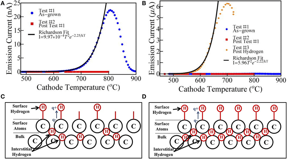
Figure 2. The thermionic emission performance between an (A) as-grown nitrogen-incorporated diamond sample and (B) the same sample following exposure to a low energy hydrogen plasma. It was found that this hydrogenation treatment significantly increased the thermionic emission current, primarily through improvement in the emitter’s Richardson constant. It is hypothesized that these results are due to an increased surface and bulk hydrogen concentration upon hydrogenation. Because such samples are grown in a hydrogen-rich environment, there is likely a small amount of hydrogen present in the bulk and on the diamond surface (C). As hydrogen lowers the electron affinity (and thereby the work function) of diamond, the majority of emission will arise from these surface sites. Upon hydrogenation, surface hydrogen concentration increases leading to more sites for emission (D). In addition, the increased bulk hydrogen concentration decreases the sample’s resistivity, allowing for a larger flux of electrons traveling normal to the surface. This explanation appears to account for the large observed increase in Richardson constant with little change in work function following hydrogenation. (A,B) Reprinted with permission from Paxton et al. (2012). Copyright 2012, American Vacuum Society. (C,D) Images provided courtesy of W. F. Paxton.
Nanotips/1D Materials
Carbon nanotubes are the signature 1D material that show low electrical resistivity and strong field electron emission at a low applied field (Saito et al., 1997). However, they exhibit a relatively high work function, but in combination with a low work function material such as p-type, B-doped diamond, can provide an ideal configuration for specific emitter applications. New deposition approaches have been developed which have enabled growth of B-doped diamond on multiwalled nanotube supports (Zanin et al., 2014).
In addition to the ongoing development of emission-specific materials, a number of new advances have looked at not only reducing the work function but also enhancing emission through other mechanisms. The following list some of these recent findings.
Photon-Enhanced Thermionic Emission (PETE)
Photon-enhanced thermionic emission (PETE) is a combined emission process that couples photon absorption with thermal emission. The PETE effect for emitters that incorporate a semiconductor absorbing layer, takes advantage of both the total energy of the photon flux and the flux of photons with sufficient energy to excite electrons directly into the conduction band of the emitter (Schwede et al., 2010, 2013). The effect provides a substantial enhancement of the emitter current density for moderate temperatures (i.e., at temperatures below the point where pure thermionic emission dominates). The PETE effect has been reported for gallium nitride:cesium surfaces and for silicon/diamond double layer structures (Schwede et al., 2010; Sun et al., 2014). The role of surface and interface recombination has also been explored in III-V heterostructures (Schwede et al., 2013). PETE-like behavior has also been observed in carbon nanotube arrays (Vahdani Moghaddam et al., 2015).
NEA Emitters/Collectors to Mitigate Space Charge
Research has established that reducing the vacuum level below the conduction band minimum (i.e., a NEA surface) should reduce the space-charge barrier (Smith et al., 2006; Smith, 2013). The effect is related to the kinetic energy of electrons emitted from an NEA surface, which would be greater than the value of the NEA. For example, for the H-terminated diamond surface the vacuum level is more than 1 eV below the conduction band minimum. This means that electrons emitted from the conduction band minimum would have a kinetic energy of greater than 1 eV, which could enable overcoming the space-charge potential barrier. Simulations indicated that the space-charge barrier is reduced by the value of the NEA for thermionic emission of conduction band electrons.
Heat Trap in 1D Materials
Confining applied thermal energy to a low work function thermionic emission region may prove crucial for efficient operation of certain emitter structures. Research has established that one-dimensional materials such as carbon nanotubes can readily support an extremely high-temperature gradient (in all directions) because thermal transport between nanotubes is low and thermal transport along the nanotube is limited by phonon scattering and the narrow cross-section (Figure 3) (Yaghoobi et al., 2011, 2012).

Figure 3. (A) Schematic representation of a solar electron source (not to scale). The focused sunlight induces localized heating of the nanotube forest to thermionic emission temperatures, and the anode, placed above the forest, collects the emitted electrons. Due to the “Heat Trap” effect in carbon nanotube forests, it is very easy to locally heat these conducting materials to thermionic emission temperatures using low optical powers. (B) This has enabled the recent demonstration of compact solar thermionic devices. The photograph shows the experimental setup of a solar electron source outdoors. An off-the-shelf, 50-mm-diameter lens was used to concentrate sunlight onto a ~700-µm spot on the side surface of the carbon nanotube forest (placed inside the glass vacuum tube). A Keithly 6517A electrometer was used to apply a collection voltage and measure the electron emission current (inset shows incandescence from a localized hot spot on a nanotube forest, while the surrounding areas of the forest remain cool). Adapted from Yaghoobi et al. (2012) under Creative Commons Attribution 3.0.
Molecular/Ion-Enhanced Emission
Rather than using interelectrode species to mitigate space charge in TEC, this approach employs interelectrode molecules/ions to contribute to charge transport across the gap. This process would apply to a narrow gap thermionic converter. The concept is based on forming a negative ion as a neutral molecule contacts the emitter surface, desorbing the ion so it traverses the electrode gap, and neutralizing the ion upon contact at the collector surface. The effect has been observed for atomic hydrogen and ammonia (NH3) in a thermionic converter with N-doped diamond surfaces. These molecules have negative ion bound states of about 0.75 eV, which apparently aligns with the electronic states of the doped diamond emitter. Results have indicated an order of magnitude increase in power density when hydrogen or ammonia were introduced in a diamond based TEC planar cell (Koeck et al., 2011). If thermionic convertors are operated with an ionized background gas, the charge transport from emitter to the collector by bare electrons may be replaced by transport via ions. This mechanism features the advantage that the energy levels of the atoms, molecules, or ions can be suitably matched to energy levels in the emitter or the collector to allow enhanced charge transfer between the electrodes and the gas, for example, by ion-enhanced field emission (Go and Venkattraman, 2014).
Quantum Tunneling/Thermal-Field Emission
Thermionic emission is typically represented as electrons emitted with energy above the vacuum barrier energy. However, the application of a field can enable significant emission due to barrier lowering (i.e., the Schottky effect in Eq. 2) and quantum mechanical tunneling (i.e., thermally assisted tunneling). Studies have indicated that nano protrusions can result in enhanced thermionic emission attributed to tunneling effects and barrier lowering (Spindt et al., 1976; Barmina et al., 2012).
Future Needs and Opportunities
While there has been significant progress in the development of emitter materials as well as new approaches to enhancing emission, there still remain significant barriers to implementing these materials in functional TEC devices with high performance and long lifetimes. We point to a few areas of future research that could help bridge this gap.
Emitter Materials and Coatings
There has been significant progress in the last decade in the search for new low work function materials such as the NEA wide-bandgap semiconductors of diamond, BN, and AlN (Powers et al., 1995; Nemanich et al., 1996). Stable NEA surface terminations would substantially impact the applicability of these materials in TEC applications. Initial reports suggest termination with monolayer metal oxides may be appropriate for diamond. In fact, monolayer and bilayer terminations that optimize the surface dipole may impact a larger group of materials, which could include carbides and other ceramic materials. Recent developments in atomic layer deposition of thin oxides could be timely for these emerging materials. Single crystal or large grain polycrystalline substrates may achieve significant improvements in stability and efficiency, and the role of defects or impurities could be more carefully established.
Comprehensive Theory/Simulation of Emission
While the development of materials has taken center stage, there is still much about the fundamental aspects of thermionic emission that remain unresolved. For example, the Richardson coefficient A is still predominantly only determined by empirical curve fitting and cannot be well predicted theoretically for most materials (Hatsopoulos and Gyftopoulos, 1979). Going forward, the role of theory and simulations has a two-fold challenge: (1) to relate the materials properties to emission, stability, and account for new mechanisms such as PETE, NEA, and quantum effects and (2) to provide guidance on system-level effects that include thermal transport, photon coupling, and overall system operation characteristics. For specific materials, providing a fundamental understanding of the surface work function and Richardson constant for different surface terminations and materials will be crucial. The development of a database of materials and surfaces with theoretical underpinning could also have a profound impact for guiding the development of new systems. One example of using quantum mechanical calculations for nanotip emitters is shown in Figure 4.
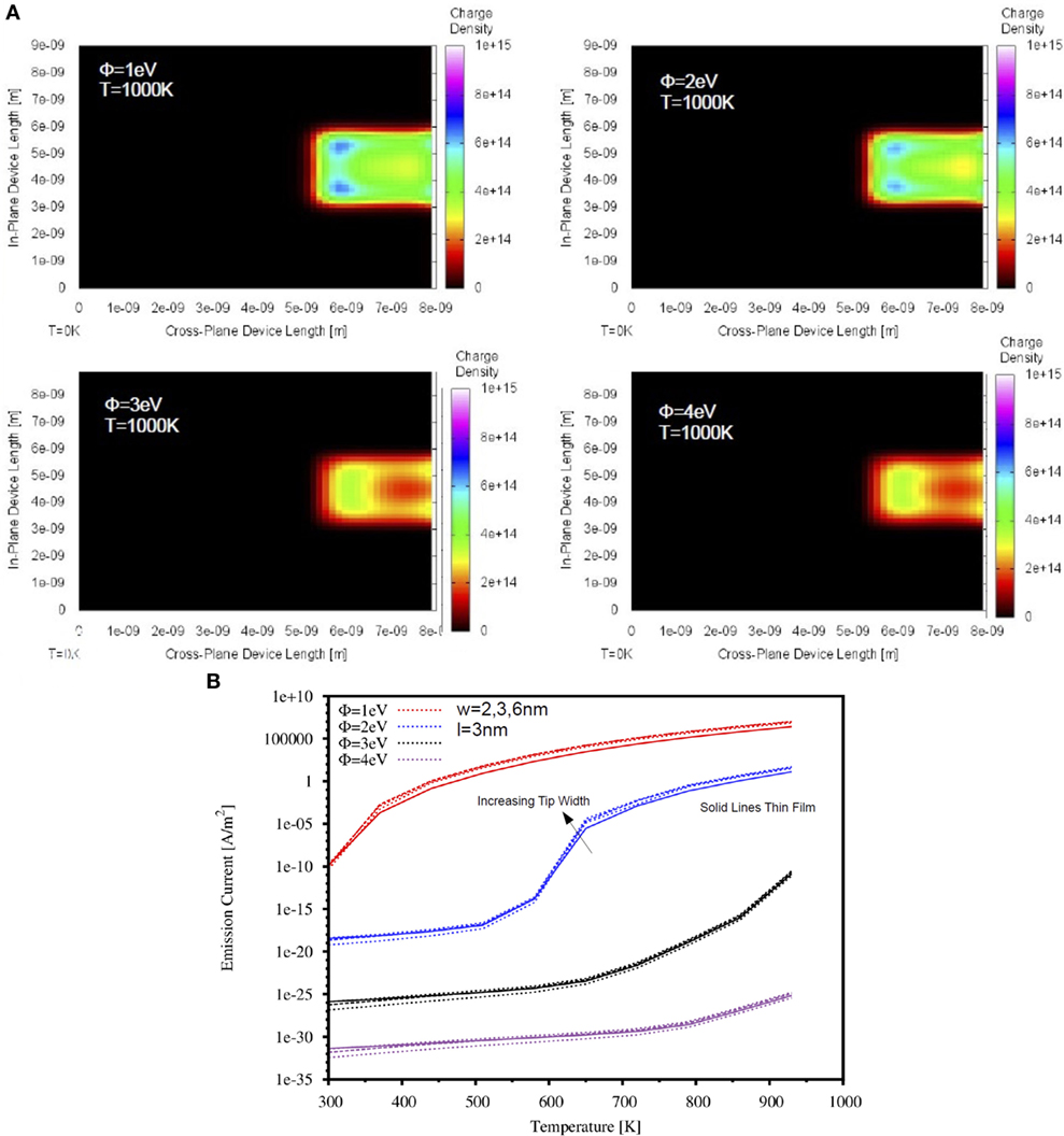
Figure 4. A non-equilibrium Green’s function model was used to investigate emission current as a function of tip length and width. (A) The calculated local density of states for several work function materials. (B) The lower plot is the emission current for a series of tip widths. Dashed lines include a tip, and solid lines are thin-film results. Images provided courtesy of T. Musho.
New Emission Mechanisms
A number of new emission mechanisms mentioned earlier are at very early stages of understanding or even proof-of-concept. Photon-enhanced thermionic emission (PETE), NEA for space-charge barrier reduction, quantum tunneling from nanostructures, thermal energy focusing with 1D materials, and ion formation charge transport all appear to have significant advantages for specific configurations. Research is necessary to match these new mechanisms to the new materials noted above. This process should be advanced in a coordinated way with theory and simulations. Further, many of these ideas challenge the traditional concept of thermionic emission that is based on a heated simple metal. Just as semiconductor electronic and optoelectronic devices consider bands and contributions from specific electronic states and vibrational modes, there may well be opportunities to quantum engineer specific electron transport states that could enhance the efficiency of a TEC system.
Electrode Gap
Requirements
The electrode gap is the region where essential electron transport takes place and, as such, can significantly affect TEC performance. By their Coulomb charge, the electrons traversing from the emitter to the collector give rise to a negative electrostatic potential that repels other electrons. This potential may easily reach several volts. As it scales with the electron density, it is large at high current densities and is enhanced by small carrier velocities. As noted earlier, for example, if the electron density in the gap exceeds a critical limit, the negative space charge adversely affects the emission current as described by the Child–Langmuir law (Child, 1911; Langmuir, 1913). In a standard diode configuration operated in vacuum, this space charge prevents electrons from leaving the emitter, and thereby suppresses the emitter–collector current to vanishing values. Mitigating the space-charge effect has been the main problem for applications of thermionic convertors by halving their efficiencies and thus preventing their terrestrial use (Moyzhes and Geballe, 2005). It is astounding that for a century, the existence of mundane space charges was the single impediment to developing applications of the possibly highly efficient thermionic process.
In addition to space-charge effects, thermal coupling across the gap is a critical loss channel for thermionic convertors. Thermal coupling is predominantly caused by thermal radiation, which for d > ~1 μm is independent of the emitter–collector spacing d because near-field radiation effects are negligible for those spacings (see, e.g., Lee et al., 2012a). Thermal coupling is also provided by thermal conduction along parasitic channels, if those exist, such as along spacers mounted between the emitter and collector. For convertors operated with a background gas pressure or a plasma, thermal transport by these gases adds to the thermal coupling.
The need for a well-defined and uniform gap that is stable at operation temperature throughout the thermionic convertor’s lifetime constitutes one of the more significant challenges in the design of thermionic convertors. Warping and bending of the emitter and collector and changes of the gap width during heating can cause catastrophic contacts between the emitter and the collector as well as, less severely, inhomogeneous temperature and current distributions. For efficiency and longevity, these inhomogeneities obviously need to be limited. If present, swelling of nuclear fuel can furthermore aggravate the complexities of maintaining a stable gap.
Pressing the emitter and collector electrodes against spacers separating the two electrodes allows one to keep them both aligned and at a desired distance at all temperatures. Candidate materials that may be used for the spacers at high temperatures and with large temperature gradients are, e.g., silicon dioxide (SiO2) and aluminum oxide (Al2O3). The spacer density needs to balance acceptable flexure of the electrodes with the thermal losses. Reactions or interdiffusion between the spacers and the electrodes, in particular the emitter, must be tolerable. For the lifetime of the convertor, the spacers that are subjected to a large temperature gradient have to be electrically insulating in their bulk and at their surfaces, in contact to the electrodes, and in the working atmosphere, the charging of the spacer could become an issue. As the thermal conduction of the spacers scales with their area and inversely with their length, fewer spacers and larger emitter–collector distances are desirable for smaller heat losses.
Current State-of-the-Art and Recent Advances
Historically, much attention has been paid to mitigating space-charge effects and creating highly uniform electrode gaps. The following summarizes many of these past efforts as well as some more recent strategies that have significant potential.
Interelectrode Plasma
As it had previously not been possible to solve the space-charge problem without compromising the efficiency of the convertors, an alternative strategy has been to introduce positive ions into the electrode gap to neutralize the space-charge effect (Baksht et al., 1978), accepting the significant drawback in an efficiency reduction of ~30–50%. Because the ion velocity is much lower than the electron velocity, a proportionally smaller ion current suffices to neutralize the electron charges. Cesium cations (Cs+) have been found to be the ion of choice, as Cs has a small ionization energy (3.9 eV). Also, Cs characteristically lowers the work function of the collector, which is a considerable advantage. Less attractively, the work functions of all other surfaces on which the Cs is deposited are lowered, too, possibly causing problems with undesired electron emission processes and a less-than-optimal emitter work function. The required continuous supply of Cs requires a Cs reservoir, which limits the lifetime of the convertor if the reservoir cannot be replenished. The TOPAZ reactors’ Cs supplies of ~1 kg limited their lifetimes to ~1 year. For the ionization process of the Cs, various approaches have been explored, of which ionization by a low-voltage arc discharge of the Cs vapor was the only one used. The power required to maintain the discharge cuts the efficiency of such convertors by 30–50% (National Research Council, 2001; Moyzhes and Geballe, 2005). Recently, it was therefore proposed to generate the Cs+ for space-charge compensation by a suitable combination of a grid electrode and an applied magnetic field (Moyzhes and Geballe, 2005). This ionization procedure deserves experimental exploration, as it has been designed to require less energy than the state-of-the-art low-voltage arc discharge. Owing to the small efficiencies caused by Cs ionization, terrestrial use of thermionic convertors has not been pursued.
Microscale Electrode Gaps
The second approach that has been recognized to offer a solution to the space-charge problem is to place the emitter and collector so close together that the emitter–collector gap is too small for a sufficient number of electrons to accumulate and generate a detrimental space charge. For this, emitter–collector distances of less than ~5–10 μm (National Research Council, 2001) are required and have to be maintained with tight tolerances. A mechanically stable electrode support structure proved challenging to build and was found to conduct too much heat from the emitter (National Research Council, 2001). Nevertheless, by 2001 a thermionic convertor with a 6 µm gap had been built in Russia and found to work well, but be mechanically unstable (National Research Council, 2001). Therefore, modern microfabrication and semiconductor-fabrication technologies are now being explored to stabilize these distances with spacers that withstand the operation temperature and the large temperature gradients between emitter and collector (Lee et al., 2012b,c, 2014; Belbachir et al., 2014). This is facilitated by using modular convertor structures composed of relatively small emitter–collector assemblies. Test assemblies with lateral sizes of 500 µm have been fabricated (Lee et al., 2012b,c, 2014) and successfully demonstrated to remain stable for several hours at 900–1,400 K (d = 100 µm). Moreover, tests were conducted at d = 1.6 µm with microbead-type spacers (Littau et al., 2013). In Belbachir et al. (2014), an emitter–collector spacing of d = 10 µm was realized by using SiO2 spacers separating SiC and Si wafers with an effective area of 7 mm × 20 mm, albeit still with very large thermal losses through the spacers (~0.4 W/K for TE ~830°C and TC ~370°C).
Interstitial Gate Electrodes
The third approach to solving the space-charge problem is to use an additional electrode, a gate or grid, to disperse the space-charge cloud by moving the electrons from the cloud into the collector. In the past, this method was found to be unsuccessful (Hatsopoulos and Gyftopoulos, 1973). However, in 2013, thermionic convertors were demonstrated in which the space-charge problem was solved in an ion-free approach by dispersing the space-charge cloud with a positively charged gate (Figure 5) (Meir et al., 2013). Gate currents need to be suppressed, which can be done by applying magnetic fields or using electron-transparent gate materials (Wanke et al., 2016), the latter offering the possibility of realizing convertors of extremely small weight. This version of thermionic power conversion is called thermoelectronic power generation, as it is independent of the emission mechanism and furthermore uses only electrons, no ions, as active particles (Meir et al., 2013; Wanke et al., 2017). In thermoelectronic devices, optimal emitter–collector distances are on the order of 100 µm. Whereas gate losses and, possibly, the generation of magnetic fields by permanent magnets or high-TC superconducting coils deserve consideration, the gate electrode offers tunability of the devices, for example, for an electronic adjustment of the output power or emitter temperature. Thermoelectronic convertors are promising candidates as they do not require a Cs plasma, yet work with large emitter–collector spacings such that they feature durability, relative robustness, and operation also at very high emitter temperatures.
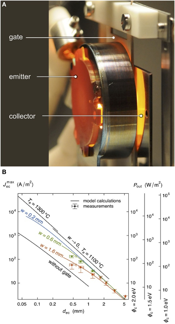
Figure 5. Using gates to solve the space-charge problem. In thermoelectronic generators as shown in panel (A), a gate voltage allows efficient operation at large emitter–collector spacings, dec. (B) Measured data (data points) together with the results of numerical simulations (lines) for various hole diameters (w) of the gate. Adapted from Meir et al. (2013) under Creative Commons Attribution 3.0.
Future Needs and Opportunities
These recent advances in device design that take advantage of new microfabrication capabilities have opened up the possibility of overcoming the space-charge challenge that has historically plagued TEC devices. Yet, additional work is required to bring these and other new ideas to fruition in practical operation. We summarize a few opportunities in the future that are needed to make this happen.
Microscale Electrode Gaps
The availability of microfabrication and semiconductor-fabrication technologies as well as the advancements of materials science afford great opportunities for the fabrication of integrated thermionic convertors with microscale electrode gaps. First, test devices with microscale gaps have been built and explored via semiconductor technologies (Lee et al., 2012b,c, 2014; Belbachir et al., 2014). The next big steps will be the demonstration of efficiency and performance under real operating conditions. The use of vacuum-encapsulated wafer technologies affords new opportunities for modular, lightweight designs, which in principle might also be fabricated in a cost-effective manner. As the devices are built with little mass, they can be robust and cost-effective, as is characteristic for MEMS-type devices. Further, emitter and collector assemblies can be fabricated by standard thin-film processes, and the possibilities for the design of devices with microscale gaps are tremendous. These need to be pursued as possible routes to devices with small thermal losses and the desired long-term stability.
Interstitial Gate Electrodes
Like for devices with microscale gaps, the use of microfabrication and semiconductor-fabrication technologies is being explored for thermoelectronic devices to integrate gate electrodes in devices with larger emitter–collector distances (~100 μm). Model calculations show high efficiencies at these large emitter–collector spacings, which still must be demonstrated experimentally. One key issue is the design of the gates such that they allow high electron transparency and thereby feature small gate currents to minimize gate losses. Another key issue is establishing techniques to fabricate integrated devices with the desired emitter–collector spacings and small thermal losses. The use of optimized materials for the gates, microscale structuring of the gates, and possibly of magnetic fields offer opportunities to realize such devices in flip-chip-based semiconductor technology. In such devices, nanostructuring of the emitter or collector electrodes may be used to match the gate microstructure for optimal device performance, for example, by channeling electron emission through the gate holes.
New Ideas and Research Fields
As noted in Section “Current State-of-the-Art and Recent Advances,” one new and novel concept for emission is the use of atoms or molecules to transport charges from the emitter to the collector. This radically new concept demands exploration of its advantages, in particular its possible synergy with microplasmas or low-temperature plasmas (Go and Venkattraman, 2014). Fundamental questions concerning energy transfer between the electrodes, losses, and the role of space charges are yet to be investigated. Like with microfabrication technology, great advances have been made in recent years in the science of microplasmas (Becker et al., 2006). New and promising ideas to reduce these losses by optimized plasma generation have been presented (Moyzhes and Geballe, 2005), but to the best of our knowledge have not yet been explored experimentally. Owing to the small emitter–collector distances of thermionic convertors, the handling and optimization of plasmas confined to the emitter–collector gap is challenging. Today’s knowledge about microplasmas may be applied to design new ignited Cs-based convertor architectures, possibly even in a pulsed mode, or to develop completely new concepts for plasma-based space-charge neutralization.
Theory and Simulation of Transport
The principles of electron motion in space, of heat transport, and of plasma discharges have long been known. In recent years, however, three-dimensional simulation software has started to offer tremendous advantages in the design of thermionic convertors, as the behavior of space charges in inhomogeneous electromagnetic fields is difficult to assess otherwise. Although existing code has already proven helpful, further advances are nevertheless required. It would be beneficial if codes were available that are able to simulate the performance of convertors on the system level. This has to be based on the calculation of the electron motion in the space charge arising from large numbers of electrons emitted through a process characterized by their thermal energy distribution and moving in inhomogeneous electromagnetic fields. To assess device performance on a system level, it is mandatory that such codes integrate all physical processes, the electron transport together with the generation, distribution, and flow of the thermal energy. Such algorithms need to be iterative, and the demand on their numerical precision is high, as the velocity spread of the electrons can be considerable, as can be the spread of length scales, in particular if emission and absorption processes on nanostructured surfaces are to be taken into account. For thermionic convertors that utilize a plasma or a gas, precise calculation of the device performance is even more demanding. Note that it is not unknown aspects of physics that challenge the simulation, nor is it that algorithms are in principle unknown. Rather, it is the large number of particles and the multitude of length and time scales involved that prohibit a good simulation of a high-performance power convertor with a macroscopic side length.
Collection
Requirements
The collector in a TEC device is often the most overlooked component, yet it still directly impacts the overall performance of the thermionic convertor. For typical TEC configurations, the maximum power is obtained when operating at a voltage equal to the difference of the emitter and collector work function as shown in Eq. 4. Consequently, there is a strong advantage to having a low work function collector. For typical operation, electrons are collected in states above the collector work function, and thermalization to the collector thermal distribution is a primary mechanism for emitter-to-collector heat transfer. Tunneling into states below the vacuum level may prove to be an advantage in reducing this loss mechanism. Absorption of thermal radiation from the emitter is the second major source of heat transfer, and a high-infrared reflectivity of the collector may enhance the system efficiency. In some operating conditions, back emission of electrons from the collector will contribute to the space-charge barrier. Evidence suggests that an NEA surface on the collector may reduce the space-charge barrier. The collector’s electrical resistance also contributes to system power loss, and reduced thermal conductivity may limit the emitter–collector temperature difference. A high Richardson constant is presumed to indicate a low value of the electron reflectivity at the collector surface; consequently, a high value is desired. However, if the Richardson coefficient is too high, then back emission from the collector can reduce efficiency; so there needs to be an optimal intermediate value. Table 2 summarizes some of these requirements necessary for a high-performance collector.
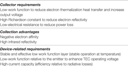
Table 2. Collector requirements and advantages, and device-related requirements.
Current State-of-the-Art and Recent Advances
Much like the emitter, many of the challenges with collectors can be narrowed down to materials challenges. However, the collector has generally received far less attention than the emitter. Still, the following overviews both historical and more recent approaches in collector design.
Collector Materials
Most of the materials noted in the emitter Section “Emission” can also be engineered for application as collector surfaces. The scandate and phosphorus-doped, n-type diamond surfaces exhibit the lowest work functions for non-cesiated surfaces reported to date (Koeck et al., 2009). In fact, they may be the lowest overall, and these surfaces could provide significant advantages for specific TEC configurations. Scandium oxide films integrated with a porous metal could provide both the low work function and low electrical resistance required for effective collector operation in a TEC system (Gibson et al., 1989). Reports have indicated a thermionic work function of 0.9 eV for phosphorus-doped diamond polycrystalline films (Koeck et al., 2009) as well as a very low Richardson constant. The 0.6 eV phosphorus-donor level suggests a lower work function may be achievable. However, the results were deduced from thermionic emission rather than collection.
Collector Mechanisms
Recently, it has been proposed that a grid structure near the collector surface could enable electron tunneling into states below the vacuum level (Figure 6) (Pan et al., 2014). This effect could lower the effective work function and increase the efficiency through reducing thermalization heat transfer. Simulations have also indicated that an NEA collector would result in a substantial reduction of the space-charge barrier (Smith, 2013). Back emission is more complicated for semiconductor surfaces, and whether it becomes important still needs to be addressed.
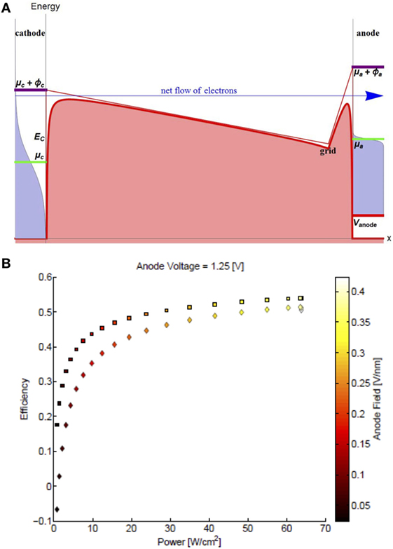
Figure 6. (A) Energy-level diagram of a single-collector-grid heat engine, where the hot side is a classical thermionic cathode emitter, and there is a strong electric field (preferably >0.1 V/nm) applied on the collector. The red region depicts the potential energy landscape in the vacuum gap, shaped by the grid voltage. Cathode-emitted electrons with energies above-but-close-to the collector Fermi level (green line) can tunnel through the thin barrier setup by the electric field outside the collector, circumventing the collector work function (purple line). (B) Predicted power vs efficiency of single-collector-grid thermionic convertor that uses inverse tunneling of electrons at the electron collector, with temperatures TH = 1,500 K, TC = 300 K, work functions ϕc = 2.0 eV, ϕa = 1.5 eV, and a varying collector electric field <0.4 V/nm. The lower curve corresponds to 1% grid loss. Reprinted, with permission, from Pan et al. (2014). Copyright 2014 IEEE.
Future Needs and Opportunities
There have been few studies of materials properties for collector applications, and they are usually coupled to a specific emitter in a TEC configuration. While many aspects of the collector surface can be deduced by analogy from emitter characteristics, it would appear that focusing on collector performance may lead to much more well-defined optimal characteristics.
Comprehensive Theory/Simulation of Collection
It will be essential to provide a fundamental understanding of how the Richardson constant impacts electron collection and, moreover, whether the Richardson constant can be optimized with different surface terminations. The development of a database of materials and surfaces with theoretical underpinning would be crucial for guiding the development of new systems. At a system level, simulating thermal properties will be required.
Collector Materials and Surfaces
The research on emitter materials has uncovered several candidate collectors with some of the lowest reported work functions. New research should focus on enhancing the electron absorption (i.e., minimizing electron reflection), and it would seem that surface terminations should play an important role.
New Collector Effects
A theoretical study has suggested that an NEA collector surface could reduce the space-charge barrier (Smith, 2013). There are opportunities to expand the study to determine the relation to specific materials configurations and to provide experimental verifications. Similarly, there is an opportunity to understand the role of quantum tunneling at the collector surface.
Integrated Collector Designs
Particular focus for integrated collector design would be on grid or nanostructures to enhance tunneling effects and to integrate efficient cooling to control the system temperature.
New Concepts and Integrated Approaches
Quantum tunneling and NEA surfaces are two new concepts that merit further study. As noted in Section “Future Needs and Opportunities,” contributions from specific electronic states and vibrational modes may well provide opportunities to quantum engineer specific electron transport states that could enhance the efficiency of the collector and the TEC system.
Going Forward
The previous sections have outlined specific areas of research need at the individual component level. However, beyond improving and optimizing individual components, there remains system-level challenges that the TEC research community must overcome.
Standards in Characterization and Testing
Given that TEC technology has not yet reached a state of widespread adoption, a complete set of standards has not been fully established for testing all aspects of fabricated devices or characterizing the materials used in various device components, although worthwhile progress has been made in defining a figure of merit for convertor performance (Shefsiek, 2010). In this section, we will first review the main requirements for characterization and testing in thermionics, then describe the current state-of-the-art, and finally discuss the future needs and some of the opportunities available for further research and development.
Materials Characterization
A thorough understanding of the properties of the materials used for the emitter, collector, and other parts of the device is crucial to be able to optimize device design and performance. A critical parameter for both the emitter and the collector is the work function and, generally speaking, materials with very low work function or even NEA are required. The work function, however, is a rather difficult property to deal with. It not only depends on the atomic composition and structure of the bulk but is also heavily influenced by the surface morphology and any type of coating, both intentional and unintentional. Moreover, work function depends on temperature, for instance due to thermal expansion (Olawole and De, 2016), and this could be particularly important for thermionic convertors, given the elevated temperatures in use.
The thermal conductivity and electrical conductivity are other important considerations. The thermal conductivity plays a direct role in determining the operating temperature and also partially determines the undesirable heat transfer from the emitter to the rest of the structure. One may argue that, unless high-frequency pulsed operation is needed, a low thermal conductivity is desired for the emitter to minimize unwanted heat transfer to the surroundings, especially in applications where it is possible to directly heat the emitter surface, such as in solar thermionics. For the collector, the situation might be the opposite since the heat load deposited by the incoming electrons needs to be removed. For both the emitter and the collector, a high electrical conductivity is needed and, naturally, this usually comes at the price of a high thermal conductivity, which could be detrimental to the operation of the emitter. Therefore, it is important to have accurate data for these conductivity values and their interdependencies as a function of temperature. Such data are not always available in the literature for the temperature ranges in question.
Similar to the work function, another parameter that directly influences the emission current is the Richardson constant for the specific material used; this “constant” can, in fact, be different for different materials. Perhaps even more crucially, the physics of emission may be different in novel materials with reduced dimensionality and modifications to the Richardson–Dushman law may be needed (Liang and Ang, 2015). The material’s melting or ablation point and its structural integrity at high temperatures, as well as its thermal expansion coefficient, are other important factors.
Arguably, there already exist various techniques to characterize all material properties of interest, ranging from high-resolution electron and scanning probe microscopy/spectroscopy for structural and surface morphology studies, to four-point probe measurements of electrical conductivity as well as current–voltage measurements (Richardson plots), Kelvin probe, and ultraviolet photoemission spectroscopy for the investigation of work function. However, almost all of these are essentially limited to ex situ materials characterization scenarios and do not necessarily allow the direct measurement or extraction of properties under actual device operation or even emulated operating conditions (such as at very high temperatures). Given the importance of in situ materials characterization as discussed before, this can represent a significant limitation.
Device Characterization
There are two aspects to device testing and characterization: one involves the measurement of the external or performance parameters. Depending on the particular application at hand, the important parameters could include maximum input power, operating temperature, output power, power per unit volume or mass, output current, current density, output voltage, output impedance, power conversion efficiency, robustness (for example, to ionizing radiation), stability, and lifetime. The other aspect of device characterization is related to measuring and monitoring the internal device parameters such as the surface temperatures of the emitter and the collector, the electron and ion (if applicable) current and their spatial distribution in the gap region, the voltage drop across different components and contact points, and the mechanical stress build-up in various regions of the device. Understanding these is crucial in the evaluation of a particular design or prototype and its subsequent improvements. It is, therefore, necessary to have the ability to characterize these properties in situ (during device operation or at least under representative conditions).
As far as device operation itself is concerned, standards for performing and reporting measurements, which would allow for meaningful comparisons across a wide variety of devices, need more attention, such as the concept of barrier index as a figure of merit (Shefsiek, 2010). Such concepts will allow the reemerging thermionics community to communicate advances more succinctly and effectively. Similarly, comparing devices that operate using different types of input power—waste heat, nuclear, solar, etc.—is not trivial.
System-Level Characterization
In practice, a thermionic convertor will inevitably be used in a larger system, at a minimum including a source of input power and a load, if not being part of a more elaborate power grid with dynamic load properties and time-varying requirements, and including sophisticated power electronic circuitry. Measures need to be developed for analyzing the cost per unit of energy or power generated, the scaling behavior/potential of the device, and possible safety concerns arising from high-power or high-temperature operation or the usage of toxic materials in device construction.
For photovoltaics and thermoelectrics, which are already in widespread deployment compared with thermionics, standard test apparatus/facilities and parameters are already in use. Examples include solar simulators and the National Renewable Energy Laboratory test facility, or the figure-of-merit (ZT) parameter. If progress in thermionic convertors is to be accelerated, which will inevitably require the participation of many researchers from various backgrounds and geographical locations, effective communication of results and comparison of obtained performance data are crucial. This necessitates the development of not only standard test equipment and central facilities but also well-defined performance reporting criteria. For instance, which one is a more meaningful parameter to be compared: power density or total power? And, if it is the former, how is it exactly defined? Similarly, should device efficiency be reported as a function of emitter temperature, or that of the temperature difference between emitter and collector, or is it simply the maximum efficiency that matters? The list goes on. The answer to many such questions is far from trivial or even unique, and requires careful thinking, deliberation, and consensus building.
Comprehensive Theory of Device Operation
Existing models and theoretical studies are typically confined to a sub-section of a thermionic convertor, such as electron emission from the emitter or transport through the gap. If an all-encompassing theory/model could be developed that includes all aspects of operation from emitter heating to power delivery to the load, it might allow the extraction of many of the device parameters and constituent material properties through simple and routine device characteristic (external/performance parameter) measurements. For example, the different regions of the current–voltage characteristics of a thermionic device—the retarding mode, the space-charge mode and the saturation mode—are sensitive to various device and material parameters in different ways. Therefore, using an accurate model for the current–voltage characteristics, one could extract multiple parameters such as the emission spot area, temperature, and work function by fitting the model predictions to current–voltage sweeps (Khoshaman et al., 2015). Similar approaches may be used for extracting other internal device parameters, too.
New Ideas and Areas
It is not a coincidence that research in TEC has recently been attracting increasing levels of interest. The technological advances of the last few decades, in particular in micro/nano materials and fabrication processes, have given us many of the tools needed to finally implement long-existing device ideas with the required material and structural properties to achieve practically useful performance levels. With the advent of such technologies, two other developments have taken place, which could have a major impact on TEC: the ability to structure materials and engineer material properties previously unthinkable when traditional thermionic designs were being implemented half a century ago, and new physical phenomena that could open up opportunities for radically new device concepts.
The creation of nanostructured emitters that take advantage of the promising properties of nanotubes and nanowires, the development of novel grid structures to minimize space-charge effects (Meir et al., 2013), molecular/ion-enhanced emission (Koeck et al., 2011), and the use of microplasmas (Go and Venkattraman, 2014) are examples of the former, while the use of photon-enhanced thermionic emission (PETE) (Schwede et al., 2010, 2013; Sun et al., 2014), the efficient light-induced heating of one-dimensional materials through unusual heat localization (Heat Trap), which enable new possibilities for solar thermionics (Yaghoobi et al., 2011, 2012), and the combination of the thermionic and tunneling phenomena (the field-emission heat engine) to increase efficiency (Pan et al., 2014), are examples of the latter.
With such developments, however, some of the challenges and opportunities discussed above become more pronounced, while new ones also arise. For instance, in situ materials property measurements in functional devices becomes increasingly important as large temperature gradients could lead to significant variations in work function, electrical and thermal conductivities, etc. within a single component of the device. Or, the interaction between the various parts of the device, such as photon tunneling between emitter and collector at micro/nano scale gap sizes, could lead to effectively different properties that may not be inferred from data collected on isolated materials or components.
As such, not only is it now crucial to develop new experimental and in situ characterization techniques and standards but it is also imperative to create theories, models, and simulation tools that allow for the accurate analysis of the entire device in a comprehensive manner, such that solving the reverse problem, that is extracting the material properties and internal device parameters with high levels of detail and precision from measured external device characteristics, also becomes a practical reality.
Summary and Final Thoughts
Thermionic emission is over a century old—perhaps older than vacuum electronics itself. Arguably, in comparison to the “information processing” branch of electronics, which has seen enormous progress in the twentieth century, outliving vacuum electronics and replacing it with solid-state electronics except for specific applications (although with the challenges faced by solid-state devices, there is now a case for resurrecting vacuum electronics), the “energy conversion” branch of vacuum electronics has made little progress. While thermionic devices have also largely given way to their solid-state counterparts, i.e., thermoelectric devices, the latter are still far from representing a mature technology, essentially due to the difficulty of containing and controlling heat and its flow. This lag highlights the fundamental challenge of energy conversion compared with information processing using electronics, where the flow of two quantities—charge and heat—as opposed to only one—charge—is of primary concern. Vacuum, by its very nature, provides a great barrier to heat transfer—a fact that gives TEC a fundamental advantage over thermoelectrics. On the other hand, electrons are naturally found in matter, and taking them out into vacuum is a difficult and often harsh process. In addition, once they are in vacuum, making them behave the way we desire and go where needed is far from trivial, especially for low-kinetic-energy electrons with a wide energy distribution and high current density, as is often the case in thermionics. As we have seen in the previous chapter, much progress has been made on all these fronts. Emitters and collectors with low work function and good stability have been demonstrated. Microfabrication processes enable the fabrication of devices with highly accurate dimensions and gap size/structure, as well as space-charge engineering by cleverly manipulating the electric field landscape in the gap region using grid electrodes. It thus appears that many of the fundamental pieces of the puzzle are now in place for us to be able to finally produce practical devices with useful performance levels. What has been missing from the recent history of TEC research and development is a coherent effort and a strong and tightly knit community of researchers with enough resources to drive this much-needed technological development and innovation forward. Time is now ripe for such a major technological push and a concerted effort to continue to advance the fundamental science that underpins TEC.
Author Contributions
DG, JH, and JG contributed to Sections “Introduction,” “Background and Fundamentals,” and “Summary and Final Thoughts.” JM, RW, AN, and RN contributed to Sections “Challenges and Recent Advances” and “Going Forward.”
Conflict of Interest Statement
The authors declare that the research was conducted in the absence of any commercial or financial relationships that could be construed as a potential conflict of interest.
Acknowledgments
The authors would like to acknowledge all participants at the 2014 Workshop on Thermionic Energy Conversion for Space and Terrestrial Applications, and especially William F. Paxton, Terrence Musho, and Tony Pan for providing Figures 2, 4 and 6, respectively. DG acknowledges the National Science Foundation under Grant Number 1254273. JH acknowledges support from both the National Aeronautic and Space Administration under NASA’s Space Technology Research Fellowship, Grant Number NNX13AL78H, and the Arthur J. Schmitt Society through the Arthur J. Schmitt Presidential Fellowship. AN acknowledges financial support from the Natural Sciences and Engineering Research Council of Canada (RGPIN-2017-04608, RGPAS-2017-507958, SPG-P 478867), the Canada Foundation for Innovation, the British Columbia Knowledge Development Fund, BCFRST/the British Columbia Innovation Council, and the Peter Wall Institute for Advanced Studies. This research was undertaken thanks in part to funding from the Canada First Research Excellence Fund, Quantum Materials and Future Technologies Program. AN also acknowledges CMC Microsystems for the provision of products and services that facilitated this research. RN acknowledges the support of the Office of Naval Research through grant N00014-10-1-0540.
References
Aamodt, R. L., Brown, L. J., and Nichols, B. D. (1962). Thermionic emission from molybdenum in vapors of cesium and cesium fluoride. J. Appl. Phys. 33, 2080–2085. doi:10.1063/1.1728899
Adams, S. F. (2006). Solar thermionic space power technology testing: a historical perspective. Energy Convers. 813, 590–597. doi:10.1063/1.2169239
Baksht, F. G., Dyvzhev, G. A., Martsinovskiy, A. M., Moyzhes, B. Y., Dikus, G. Y., Sonin, E. B., et al. (1978). Thermionic convertors and low-temperature plasma. NASA STI/Recon. Tech. Rep. N 80, 17579.
Barmina, E. V., Serkov, A. A., Stratakis, E., Fotakis, C., Stolyarov, V. N., Stolyarov, I. N., et al. (2012). Nano-textured W shows improvement of thermionic emission properties. Appl. Phys. A 106, 1–4. doi:10.1007/s00339-011-6692-6
Becker, K. H., Schoenbach, K. H., and Eden, J. G. (2006). Microplasmas and applications. J. Phys. D Appl. Phys. 39, R55–R70. doi:10.1088/0022-3727/39/3/R01
Belbachir, R. Y., An, Z., and Ono, T. (2014). Thermal investigation of a micro-gap thermionic power generator. J. Micromech. Microeng. 24, 85009. doi:10.1088/0960-1317/24/8/085009
Benke, S. M. (1994). Operational Testing and Thermal Modeling of a TOPAZ-II Single Cell Thermionic Fuel Element Test Stand. M.S. thesis, Naval Post Graduate School. Available at: https://calhoun.nps.edu/handle/10945/28426
Child, C. D. (1911). Discharge from hot CaO. Phys. Rev. (Series I) 32, 492. doi:10.1103/PhysRevSeriesI.32.492
Diederich, L., Küttel, O. M., Aebi, P., and Schlapbach, L. (1998). Electron affinity and work function of differently oriented and doped diamond surfaces determined by photoelectron spectroscopy. Surf. Sci. 418, 219–239. doi:10.1016/S0039-6028(98)00718-3
Fitzpatrick, G. O., Britt, E. J., and Moyzhes, B. (1997). “Updated perspective on the potential for thermionic conversion to meet 21st century energy needs,” in IECEC-97 Proceedings of the 32nd Intersociety Energy Conversion Engineering Conference, 1997, Honolulu, HI, 1045–1051.
Fomenko, V. S. (1966). “Chemical elements,” in Handbook of Thermionic Properties, ed. G. V. Samsonov (New York: Plenum Press Data Division). p. 5–68.
Gibson, J. W., Haas, G. A., and Thomas, R. E. (1989). Investigation of scandate cathodes: emission, fabrication, and activation processes. IEEE Trans. Electron Devices 36, 209–214. doi:10.1109/16.21207
Go, D. B., and Venkattraman, A. (2014). Microscale gas breakdown: ion-enhanced field emission and the modified Paschen’s curve. J. Phys. D Appl. Phys. 47, 503001. doi:10.1088/0022-3727/47/50/503001
Grabowski, S. P., Schneider, M., Nienhaus, H., Mönch, W., Dimitrov, R., Ambacher, O., et al. (2001). Electron affinity of AlxGa1−x N(0001) surfaces. Appl. Phys. Lett. 78, 2503–2505. doi:10.1063/1.1367275
Gryaznov, G. M. (2000). 30th anniversary of the startup of Topaz—the first thermionic nuclear reactor in the world. At. Energy 89, 510–515. doi:10.1007/BF02673508
Hatsopoulos, G. N., and Gyftopoulos, E. P. (1973). Thermionic Energy Conversion Volume I: Processes and Devices. Cambridge, MA: The MIT Press.
Hatsopoulos, G. N., and Gyftopoulos, E. P. (1979). Thermionic Energy Conversion Volume II: Theory, Technology, and Application. Cambridge, MA: The MIT Press.
Jenkins, R. O. (1969). A review of thermionic cathodes. Vacuum 19, 353–359. doi:10.1016/S0042-207X(69)80077-1
Kataoka, M., Zhu, C., Koeck, F. A. M., and Nemanich, R. J. (2010). Thermionic electron emission from nitrogen-doped homoepitaxial diamond. Diam. Relat. Mater. 19, 110–113. doi:10.1016/j.diamond.2009.09.002
Khalid, K. A. A., Leong, T. J., and Mohamed, K. (2016). Review on thermionic energy convertors. IEEE Trans. Electron Devices 63, 2231–2241. doi:10.1109/TED.2016.2556751
Khoshaman, A. H., Fan, H. D. E., Koch, A. T., Sawatzky, G. A., and Nojeh, A. (2014). Nanostructured thermionics for conversion of light to electricity: simultaneous extraction of device parameters. IEEE Nanotechnol. Mag. 14, 4–15. doi:10.1109/TNANO.2015.2426149
Khoshaman, A. H., Koch, A. T., Chang, M., Fan, H. D. E., Moghaddam, M. V., and Nojeh, A. (2015). Thermionics, thermoelectrics, and nanotechnology: new possibilities for old ideas. IEEE Trans. Nanotechnol. 8, 624–632. doi:10.1109/MNANO.2014.2313172
Koeck, F. A. M., Nemanich, R. J., Balasubramaniam, Y., Haenen, K., and Sharp, J. (2011). Enhanced thermionic energy conversion and thermionic emission from doped diamond films through methane exposure. Diam. Relat. Mater. 20, 1229–1233. doi:10.1016/j.diamond.2011.06.032
Koeck, F. A. M., Nemanich, R. J., Lazea, A., and Haenen, K. (2009). Thermionic electron emission from low work-function phosphorus doped diamond films. Diam. Relat. Mater. 18, 789–791. doi:10.1016/j.diamond.2009.01.024
Langmuir, I. (1913). The effect of space charge and residual gases on thermionic currents in High vacuum. Phys. Rev. 2, 450–486. doi:10.1103/PhysRev.2.450
Lee, J.-H., Bargatin, I., Melosh, N. A., and Howe, R. T. (2012a). Optimal emitter-collector gap for thermionic energy convertors. Appl. Phys. Lett. 100, 173904. doi:10.1063/1.4707379
Lee, J. H., Bargatin, I., Gwinn, T. O., Vincent, M., Littau, K. A., Maboudian, R., et al. (2012b). “Microfabricated silicon carbide thermionic energy convertor for solar electricity generation,” in 2012 IEEE 25th International Conference on Micro Electro Mechanical Systems (MEMS), Paris, 1261–1264.
Lee, J. H., Bargatin, I., Iwami, K., Littau, K. A., Vincent, M., Maboudian, R., et al. (2012c). Encapsulated Thermionic Energy Convertor. 493–496. Available at: http://bargatin.seas.upenn.edu/uploads/Main/bargatin 2012 Hilton Head 2.pdf
Lee, J.-H., Bargatin, I., Vancil, B. K., Gwinn, T. O., Maboudian, R., Melosh, N. A., et al. (2014). Microfabricated thermally isolated low work-function emitter. J. Microelectromech. Syst. 23, 1182–1187. doi:10.1109/JMEMS.2014.2307882
Liang, S.-J., and Ang, L. K. (2015). Electron thermionic emission from graphene and a thermionic energy convertor. Phys. Rev. Appl. 3, 14002. doi:10.1103/physrevapplied.3.014002
Littau, K. A., Sahasrabuddhe, K., Barfield, D., Yuan, H., Shen, Z.-X., Howe, R. T., et al. (2013). Microbead-separated thermionic energy convertor with enhanced emission current. Phys. Chem. Chem. Phys. 15, 14442–14446. doi:10.1039/C3CP52895B
Macdonald, N. C., Chen, L. Y., Yao, J. J., Zhang, Z. L., McMillan, J. A., Thomas, D. C., et al. (1989). Selective chemical vapor deposition of tungsten for microelectromechanical structures. Sens. Actuators 20, 123–133. doi:10.1016/0250-6874(89)87110-0
McCarthy, P. T., Reifenberger, R. G., and Fisher, T. S. (2014). Thermionic and phto-excited electron emission for energy-conversion processes. Front. Energy Res. 2:54. doi:10.3389/fenrg.2014.00054
Meir, S., Stephanos, C., Geballe, T. H., and Mannhart, J. (2013). Highly-efficient thermoelectronic conversion of solar energy and heat into electricpower. J. Renew. Sustain. Energy 5, 43127. doi:10.1063/1.4817730
Moyzhes, B. Y., and Geballe, T. H. (2005). The thermionic energy convertor as a topping cycle for more efficient heat engines—new triode designs with a longitudinal magnetic field. J. Phys. D Appl. Phys. 38, 782. doi:10.1088/0022-3727/38/5/017
National Research Council. (2001). Thermionics Quo Vadis? An Assessment of the DTRA’s Advanced Thermionics Research and Development Program. Washington, DC: The National Academies Press. doi:10.17226/10254
Nemanich, R. J., Baumann, P. K., Benjamin, M. C., King, S. W., van der Weide, J., and Davis, R. F. (1996). Negative electron affinity surfaces of aluminum nitride and diamond. Diam. Relat. Mater. 5, 790–796. doi:10.1016/0925-9635(95)00485-8
Nemanich, R. J., Bilbro, G. L., Bryan, E. N., Koeck, F. A., Smith, J. R., and Tang, Y. (2010). “Thermionic and field electron emission devices from diamond and carbon nanostructures,” in 2010 IEEE 3rd International Nanoelectronics Conference (INEC), Hong Kong, 56–57.
Norris, W. T. (1964). Work function of the (110) face of tantalum in a cesium vapor. J. Appl. Phys. 35, 467–469. doi:10.1063/1.1713395
Olawole, O. C., and De, D. K. (2016). “Modeling thermionic emission from carbon nanotubes with modified Richardson-Dushman equation,” in Proceedings Volume 9927, Nanoengineering: Fabrication, Properties, Optics, and Devices XIII, eds E. M. Campo, E. A. Dobisz, and L. A. Eldada (San Diego, CA: International Society for Optics and Photonics), 992716-1–992716-8. doi:10.1117/12.2231357
Pan, T., Busta, H., Gorski, R., and Rozansky, B. (2014). “Inverse tunneling of electrons in field emission heat engines,” in Technical Digest – 2014 27th International Vacuum Nanoelectronics Conference, IVNC (Engelberg: Institute of Electrical and Electronics Engineers Inc), 147–148.
Paxton, W. F., Howell, M., Kang, W. P., and Davidson, J. L. (2012). Influence of hydrogen on the thermionic electron emission from nitrogen-incorporated polycrystalline diamond films. J. Vac. Sci. Technol. B Nanotechnol. Microelectron. Mater. Process. Meas. Phenom. 30, 21202. doi:10.1116/1.3684982
Powers, M. J., Benjamin, M. C., Porter, L. M., Nemanich, R. J., Davis, R. F., Cuomo, J. J., et al. (1995). Observation of a negative electron affinity for boron nitride. Appl. Phys. Lett. 67, 3912–3914. doi:10.1063/1.115315
Rasor, N. S. (1991). Thermionic energy conversion plasmas. IEEE Trans. Plasma Sci. 19, 1191–1208. doi:10.1109/27.125041
Richardson, O. W. (1921). The Emission of Electricity from Hot Bodies. London: Longmans, Green and Company.
Ristein, J. (2000). Electronic properties of diamond surfaces – blessing or curse for devices? Diam. Relat. Mater. 9, 1129–1137. doi:10.1016/S0925-9635(99)00316-7
Saito, Y., Hamaguchi, K., Nishino, T., Hata, K., Tohji, K., Kasuya, A., et al. (1997). Field emission patterns from single-walled carbon nanotubes. Jpn. J. Appl. Phys. 36, L1340–L1342. doi:10.1143/JJAP.36.L1340
Schlichter, W. (1915). Die spontane elektronenemission glühender metalle und das glühelektrische element. Ann. Phys. 352, 573–640. doi:10.1002/andp.19153521302
Schottky, W. (1914). Emission of electrons from an incandescent filament under the action of a retarding potential. Ann. Phys. 44, 1011–1032. doi:10.1002/andp.19143491503
Schwede, J. W., Bargatin, I., Riley, D. C., Hardin, B. E., Rosenthal, S. J., Sun, Y., et al. (2010). Photon-enhanced thermionic emission for solar concentrator systems. Nat. Mater. 9, 762–767. doi:10.1038/nmat2814
Schwede, J. W., Sarmiento, T., Narasimhan, V. K., Rosenthal, S. J., Riley, D. C., Schmitt, F., et al. (2013). Photon-enhanced thermionic emission from heterostructures with low interface recombination. Nat. Commun. 4, 1576. doi:10.1038/ncomms2577
Shefsiek, P. (2010). Describing and correlating the performance of the thermionic convertor: a historical perspective. IEEE Trans. Plasma Sci. 38, 2041–2047. doi:10.1109/TPS.2010.2050910
Smith, J. R. (2013). Increasing the efficiency of a thermionic engine using a negative electron affinity collector. J. Appl. Phys. 114, 164514. doi:10.1063/1.4826202
Smith, J. R., Nemanich, R. J., and Bilbro, G. L. (2006). The effect of Schottky barrier lowering and nonplanar emitter geometry on the performance of a thermionic energy convertor. Diam. Relat. Mater. 15, 870–874. doi:10.1016/j.diamond.2005.12.057
Spindt, C. A., Brodie, I., Humphrey, L., and Westerberg, E. R. (1976). Physical properties of thin-film field emission cathodes with molybdenum cones. J. Appl. Phys. 47, 5248–5263. doi:10.1063/1.322600
Sugino, T., Kimura, C., and Yamamoto, T. (2002). Electron field emission from boron-nitride nanofilms. Appl. Phys. Lett. 80, 3602–3604. doi:10.1063/1.1477622
Sun, T., Koeck, F. A. M., Rezikyan, A., Treacy, M. M. J., and Nemanich, R. J. (2014). Thermally enhanced photoinduced electron emission from nitrogen-doped diamond films on silicon substrates. Phys. Rev. B 90, 121302. doi:10.1103/PhysRevB.90.121302
Tiwari, A. K., Goss, J. P., Briddon, P. R., Horsfall, A. B., Wright, N. G., Jones, R., et al. (2014). Unexpected change in the electron affinity of diamond caused by the ultra-thin transition metal oxide films. Europhys. Lett. 108, 46005. doi:10.1209/0295-5075/108/46005
Trucchi, D. M., and Melosh, N. A. (2017). Electron-emission materials: advances, applications, and models. MRS Bull. 42, 488–492. doi:10.1557/mrs.2017.142
Vahdani Moghaddam, M., Yaghoobi, P., Sawatzky, G. A., and Nojeh, A. (2015). Photon-impenetrable, electron-permeable: the carbon nanotube forest as a medium for multi-photon thermal-photoemission. ACS Nano 9, 4064. doi:10.1021/acsnano.5b00115
van der Weide, J., Zhang, Z., Baumann, P. K., Wensell, M. G., Bernholc, J., and Nemanich, R. J. (1994). Negative-electron-affinity effects on the diamond (100) surface. Phys. Rev. B 50, 5803–5806. doi:10.1103/PhysRevB.50.5803
Voesch, W., Wanke, R., Rastegar, I., Braun, W., Kribus, A., and Mannhart, J. (2017). High-temperature latent-heat energy storage concept based on thermoelectronic energy conversion. Energy Technol. doi:10.1002/ente.201700273
Wanke, R., Hassink, G. W. J., Stephanos, C., Rastegar, I., Braun, W., and Mannhart, J. (2016). Magnetic-field-free thermoelectronic power conversion based on graphene and related two-dimensional materials. J. Appl. Phys. 119, 244507. doi:10.1063/1.4955073
Wanke, R., Voesch, W., Rastegar, I., Kyriazis, A., Braun, W., and Mannhart, J. (2017). Thermoelectronics energy conversion: concepts and materials. MRS Bull. 42, 518–524. doi:10.1557/mrs.2017.140
Wilson, V. C. (1959). Conversion of heat to electricity by thermionic emission. J. Appl. Phys. 30, 475–481. doi:10.1063/1.1702391
Yaghoobi, P., Moghaddam, M. V., and Nojeh, A. (2011). “Heat trap”: light-induced localized heating and thermionic electron emission from carbon nanotube arrays. Solid State Commun. 151, 1105–1108. doi:10.1016/j.ssc.2011.05.024
Yaghoobi, P., Vahdani Moghaddam, M., and Nojeh, A. (2012). Solar electron source and thermionic solar cell. AIP Adv. 2, 42139. doi:10.1063/1.4766942
Zanin, H., May, P. W., Fermin, D. J., Plana, D., Vieira, S. M. C., Milne, W. I., et al. (2014). Porous boron-doped diamond/carbon nanotube electrodes. ACS Appl. Mater. Interfaces 6, 990–995. doi:10.1021/am4044344
Keywords: thermal energy conversion, thermionic energy conversion, thermionic emission, heat engine, electron emission
Citation: Go DB, Haase JR, George J, Mannhart J, Wanke R, Nojeh A and Nemanich R (2017) Thermionic Energy Conversion in the Twenty-first Century: Advances and Opportunities for Space and Terrestrial Applications. Front. Mech. Eng. 3:13. doi: 10.3389/fmech.2017.00013
Received: 19 July 2017; Accepted: 17 October 2017;
Published: 08 November 2017
Edited by:
Guillermo Rein, Imperial College London, United KingdomReviewed by:
Dong Liu, University of Houston, United StatesLiang Chen, Xi’an Jiaotong University, China
Copyright: © 2017 Go, Haase, George, Mannhart, Wanke, Nojeh and Nemanich. This is an open-access article distributed under the terms of the Creative Commons Attribution License (CC BY). The use, distribution or reproduction in other forums is permitted, provided the original author(s) or licensor are credited and that the original publication in this journal is cited, in accordance with accepted academic practice. No use, distribution or reproduction is permitted which does not comply with these terms.
*Correspondence: David B. Go, ZGdvQG5kLmVkdQ==