CMOS MEMS Design and Fabrication Platform
 Sheng-Hsiang Tseng
- Taiwan Semiconductor Research Institute (TSRI), Hsinchu, Taiwan
This article mainly describes the technology related to the CMOS MEMS process platform provided by the Taiwan Semiconductor Research Institute (TSRI), including the process flow, design verification, back-end dicing, and packaging of the CMOS MEMS integrated sensing single chip. The front-end CMOS processes can be a standard 0.35 or 0.18 µm CMOS process, or even a BCD high-voltage process. Some academic designs also utilize this platform for in-house post-CMOS process. Finally, the article also explains in detail the CMOS MEMS design flowchart and implementation method provided by TSRI.
Introduction
Since the late 1990s, microelectromechanical systems (MEMS) has been actively developed toward commercialization and has been more effectively integrated into consumer electronic products. In Nintendo Wii Console in 2006 and the first-generation iPhone smartphone in 2007, MEMS sensor devices were first used in home games and mobile phones. This epoch-making idea has brought human-body sensory interaction technology into the generation of real experience. Due to the differentiation and patent protection of the sensing principles and manufacturing methods of sensors, sensor technologies employed in most products are designed and manufactured by integrated design manufacturers. The main technique for manufacturing chips involves separately manufacturing the sensor and circuit chips and then using a packaging method to integrate their functions. Compared with traditional semiconductor processing, sensor processing requires thicker films and movable three-dimensional structures; thus, the microstructure has various challenges and difficulties regarding process specifications and yields. As sensor applications become more diverse, different institutions and companies have successively developed MEMS process platforms compatible with various applications, thereby providing designers with standardized process specifications. This reduces the process variance of product development and speeds up the development time for mass production.
CMOS MEMS Design and Fabrication Platform by TSRI
The Beginning of 0.35-μm Based CMOS MEMS Process and Design Platform
Taiwan has the world’s top and numerous complementary metal-oxide-semiconductor (CMOS) foundries integrated with manufacturing and R&D capabilities for traditional integrated circuits (ICs). CMOS is the most common standard process for electronic-circuit semiconductor manufacturing. Since 2002, the Taiwan Semiconductor Research Institute (TSRI) [formerly National Chip Implementation Center (CIC)] has integrated MEMS process with the 0.35-µm CMOS process in CMOS foundry, using standardized circuit process and post-CMOS micromachining methods to fabricate MEMS sensors and related devices. MEMS and CMOS processes can be integrated in three forms: pre-CMOS (Sherman et al., 1992; Smith et al., 1995), intra-CMOS (Offenberg et al., 1995) and post-CMOS (Luo et al., 2002). The first two methods require in-house process flow adjustments to be compatible with the CMOS process, which greatly increase the manufacturing cost and process complexity. To keep the process characteristics and transistor parameters of the original CMOS platform unaffected, TSRI employs the CMOS standard process of the foundry in Taiwan as the basis and integrates an etching process with a low-temperature post-CMOS micromachining process, as shown in Figure 1. Although some research institutes have employed similar approaches (Luo et al., 2002; Xie and Fedder, 2000), only TSRI used the standardized full wafers from commercial foundries for post-CMOS micromachining process development. The back-end micromachining process requires an additional mask and thick photoresist layer deposition to determine the structural area of the sensor devices. The mask is used to define the range of dry etching and the micromechanical structure to be suspended. The front- and back-end processes are carried out by commercial foundries, and the general process flow is shown in Figure 2 (Dai et al., 2005; Tseng et al., 2010).
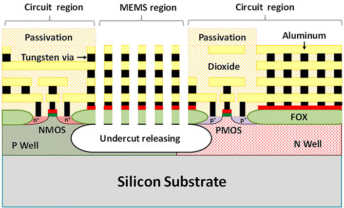
FIGURE 1. The cross-section view of CMOS MEMS process.
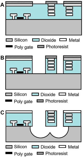
FIGURE 2. Steps of CMOS MEMS process, (A) after completion of CMOS process, (B) anisotropic dioxide etching, and (C) isotropic silicon etching to release the microstructure.
In the CMOS MEMS process platform proposed by TSRI, the sensor structure is derived from the material film stacking and combination employed in the CMOS process, and no additional materials incompatible with the CMOS process are incorporated. Because traditional materials for the CMOS process are used, more advanced CMOS processes have more metal layers and are more suitable for manufacturing sensing and actuating devices with thicker structures. Taking the 0.35-µm CMOS process as an example, there are usually four metal layers, and the overall thickness of the metal and oxide layers is about 6–7 µm. However, up to six metal layers are achieved in the 0.18-µm CMOS process, and the overall thickness is increased to 10–11 μm, which is more suitable for developing sensors with high sensitivity and driving force.
0.18-μm Based CMOS MEMS Process and Design Platform
In 2007, TSRI proposed a CMOS MEMS process platform based on the Taiwan Semiconductor Manufacturing Company (TSMC) 0.18-µm CMOS process, and the back-end process is a post-CMOS micromachining process with Asia Pacific Microsystems (APM). Based on the above process, we proposed a 5.8-GHz voltage-controlled oscillator (VCO) integrated with a CMOS MEMS high-Q inductor. Through the micromachining process, the parasitic capacitance and resistance of the original CMOS inductor were greatly reduced. In addition to improving the quality factor of the inductor by 88%, phase noise in the VCO circuit was reduced by 5 dB (Tseng et al., 2007). (Chiu et al., 2013) employed this process to design an accelerometer based on differential LC-tank oscillators. The sensor uses suspended MEMS inductance devices and interdigitated electrodes on the structure to form an LC tank. The output of the differential oscillator is mixed, and the output frequency of the mixer is proportional to the capacitance changes due to the applied acceleration. In addition, (Chiu et al., 2014) used polysilicon in the CMOS process as a piezoresistive sensor. The accelerometer has polysilicon embedded in each of the four cantilevers and is read by a CMOS oscillator circuit. The oscillation frequency of the oscillator circuit changes with the resistance when external acceleration is applied. (Tseng et al., 2008) used N-type and P-type polysilicon as thermopiles sensors, and the hot- and cold-side sensing regions of the sensor were fabricated by MEMS etching. The sensing circuit uses a differential ring oscillator to covert frequency signals. When the heater heats and causes a temperature difference between the hot and cold ends of the thermopiles, thermoelectric voltage is generated to control the bias current of the high-frequency oscillator circuit, thereby causing a shift in the output frequency.
TSRI’s CMOS MEMS design platform provides design kits, including integration of MEMS masks for front-end CMOS processes, such as technology files for Cadence’s Virtuso software and Synopsys’ Laker software, as well as CMOS p-cell library and MEMS design guideline. For process design verification, TSRI also provides Mentor’s Calibre software for CMOS MEMS process design rule check (DRC), layout versus schematic (LVS), parasitic extraction, post-layout simulation, and other related verification procedures. In addition to using the mask layer of the software and the process step to build the structure model, the designer can use the DRC rules of the process to realize and confirm the physical chip. Since the CMOS MEMS platform also integrates a back-end circuit, the parasitic capacitance of the sensing signal at the front-end of the circuit can be extracted using a CMOS design tool, which more accurately simulates and estimates the overall characteristics of the circuit and the sensor. Since the front-end CMOS process has complete and mature process quality and verification steps, die-level CMOS chips can be used with in-house micromachining processes to design and integrate sensor chips. For example, the capacitive 3-axis accelerometer proposed by (Sun et al., 2009) employs wet etching with in-house post-processing to remove the aluminum interlayer and tungsten vias in CMOS to form a vertical sensing capacitor. Then, reactive ion etching is employed to remove the lateral silicon dioxide and underlying silicon substrate to form an in-plane sensing capacitor to achieve a single proof-mass three-axis accelerometer sensor. (Liu et al., 2012) also used the in-house post-CMOS micromachining process to remove the aluminum/tungsten-via of CMOS through wet etching and supported the moveable sensor using cantilevers or membrane. Due to the effect of stress, the size of a CMOS MEMS sensor ranges from 150 to 300 μm, and the sensed capacitance change is in several to tens of femtofarad. Such a small detection signal must be directly integrated into the back-end circuit amplifier to convert and amplify the detected capacitance. Related studies include the integrated capacitive sensor array for fingerprint detection (Liu et al., 2012), capacitive ultrasonic sensor array for three-dimensional (3D) photoacoustic image (Liao et al., 2013), and capacitive squeeze-film pressure sensor (Hsieh et al., 2020).
0.35-µm Based CMOS Multioption MEMS Process
In 2014, TSRI collaborate with APM to integrate 0.35-µm CMOS MEMS with a micromachining process suitable for BioMEMS, and subsequently developed a 0.35 µm CMOS multioption MEMS process. In this process, users can choose a process combination (with/without suspended structure, with/without gold and platinum layers) according to their sensor design. Gold and platinum are chosen for the 0.35 µm CMOS multioption MEMS platform because of its biocompatibility and inactivity in liquids. Therefore, they can be used as a working electrode in electrochemical experiments. In addition, thiol-modified biomolecules can bind to gold. TSRI uses this platform to design biomedical sensors that detect DNA, protein, virus, and cells (Tsai et al., 2010).
One-Stop Multi-Project Wafer 0.18-µm CMOS MEMS Process and Design Platform
From 2002 to 2014, Taiwan academia published many research results using the CMOS MEMS platform and design services provided by TSRI. Based on the development of research attributes to commercialization, TSRI collaborated with the United Microelectronics Corporation (UMC) to develop a one-stop eight-inch full-wafer fabrication CMOS MEMS process platform. Based on experience, dry etching is still used for post-CMOS micromachining, and anisotropic dioxide layer etching and lateral isotropic silicon substrate etching are performed to release the microstructure of the CMOS process. UMC and TSRI jointly proposed a complete CMOS MEMS process and design platform (Tseng et al., 2012; Lin et al., 2013). Figure 3 shows the SEM image of the cross-section view of the CMOS MEMS process. In addition, we built a complete electronic design automation (EDA) design environment on this platform and defined DRC corresponding to the MEMS components according to the foundry process and etching specifications. Since the front-end CMOS process and post-CMOS micromachining process are performed by the same foundry (UMC), there is no process-transfer problem. Therefore, the entire CMOS MEMS process is more stable for the yield and reliability of MEMS devices and circuit.
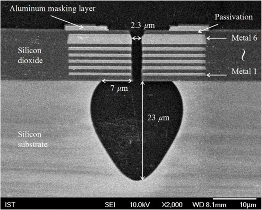
FIGURE 3. SEM image of the cross-section view of the CMOS MEMS process (Tseng et al., 2012).
Since the microstructures fabricated using the CMOS MEMS process includes a composite of dioxide layer and aluminum metal, the stress and stress gradient of the structure cannot be suppressed by post-treatment procedure, such as annealing, as in polysilicon or epi-silicon. However, in depositing thin films of different stacks in CMOS, we can choose different layer stacking to form microstructures with minimal stress-induced deformation. Therefore, TSRI uses cantilever beams of different compositions to perform in-plane and out-of-plane structural bending and deformation tests and measures and tracks the results of run-to-run and wafer-to-wafer. Stresses in film extends or contracts the release structure. To measure the stress properties of materials in CMOS, we design a rotating indicator, as shown in Figure 4A (Drienhuizen et al., 1993). The device consists of two support beams and a rotating indicator beam. One end of the support beam is fixed to the anchor, and the other end is connected to the indicator. When the structures are released by etching away the sacrificial substrate layer, two support beams are elongated or contracted due to the residual stress, which in turn rotates the indicator. According to the results of rotating the indicator beam, aluminum obtained through the CMOS process generally has tensile residual stress, and silicon dioxide has compressive residual stress. As shown in Figure 4B, we also designed a series of cantilevers with different compositions (optionally including metal-1 to metal-6 layer) to monitor the stress gradient and bending deformation of the microstructure. The length and width of each cantilever are 600 and 6 μm, respectively. In cantilevers with different compositions, the accumulation of residual stress in different thin-film layers in CMOS causes different stress gradients, resulting in different bending deformations of the cantilever. We could measure the radius of curvature of the cantilever using a white light interferometer, and with the correction of the anchor’s boundary condition, the stress gradient function of the cantilever beam with a specific composition can be obtained. As shown in Figure 5, in the 3D model of finite element software, the function of the stress gradient can be set, and then the bending deformation of the microstructure can be simulated and predicted. Thus, we can design the compensation range of the readout circuit more precisely and adjust the gain of the amplifier stage more appropriately. Furthermore, we can optimally design the microstructure by analyzing the stress gradients that produce minimal bending deformation. In our previous study (Chang et al., 2021), we implemented a three-axis accelerometer with a maximum bending displacement of less than 2 µm in a 476 μm × 660 µm out-of-plane (z-axis) sensor, as shown in Figure 6.
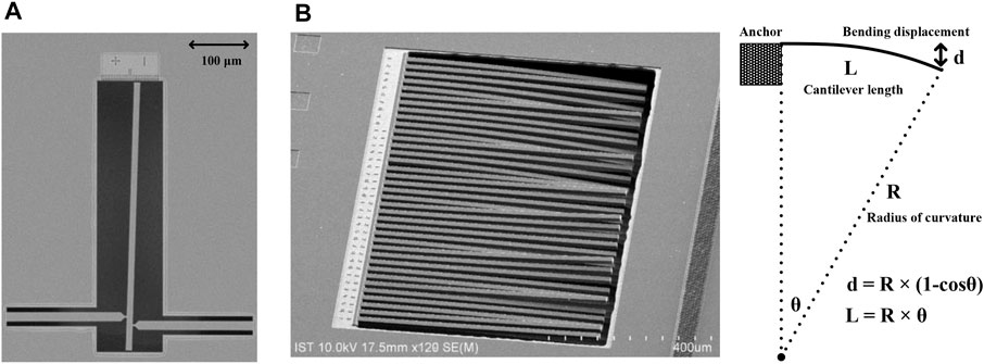
FIGURE 4. (A) SEM image of the rotating indicator. (B) Test cantilever based on the CMOS MEMS process and the relationship between stress gradient and bending deformation.
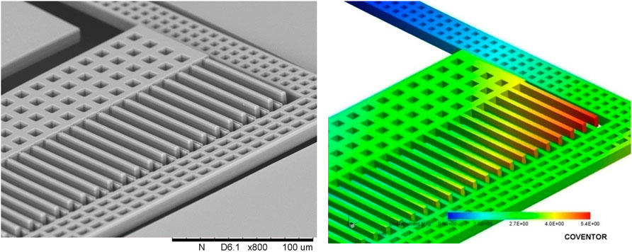
FIGURE 5. SEM image of a sensor and 3D model of the finite element software with stress gradient and bending deformation.
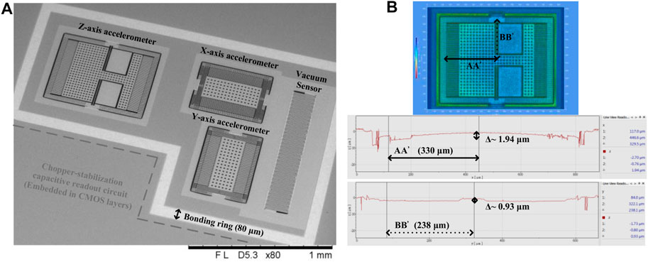
FIGURE 6. (A) SEM image of a single chip three-axis CMOS MEMS accelerometer. (B) Bending deformation of the z-axis accelerometer measured using an optical interferometer (Chang et al., 2021).
UMC’s 0.18-µm one-stop CMOS MEMS process platform has a structural thickness of about 10 µm. The photoresist has low etching selectivity over the dioxide layer; thus, aluminum and thick photoresist are used as protective layers to define the microstructure during the dioxide etching process. The minimum gap spacing for the interdigitated electrodes or metal capacitor plates in the microstructure is 2.3 µm. The post-CMOS micromachining process is completely compatible with the UMC standard CMOS process, which can mass-produce low-cost chips and is more convenient for circuit signal processing and integration. Since the platform cannot yet be used for wafer-level packaging, dies in CMOS MEMS wafer rely on dry laser technology for dicing and separation. Currently, TSRI collaborates with a packaging company to use stealth laser dicing technology for wafer dicing. Stealth laser dicing technology works by focusing a laser inside the wafer and creating a modified layer in the workpiece, then separating the chips using a tape expander (Kumagai et al., 2007). Since the cutting process is performed inside the wafer, the cutting dust of the silicon substrate is not sputtered on the surface of the CMOS MEMS wafer, which could affect the normal function of the microstructure. A diced CMOS MEMS chip is shown in Figure 7, it is compatible with various standard ceramic packages for functional testing.
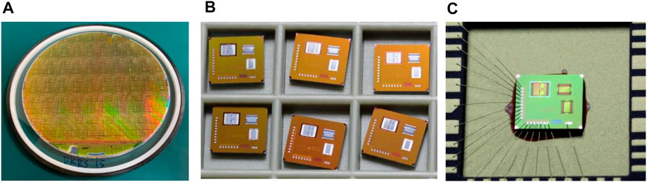
FIGURE 7. (A) UMC’s 0.18 µm CMOS MEMS multi-project wafer after stealth laser dicing process, (B) Diced CMOS MEMS chip, and (C) Wire-bonded CMOS MEMS chip in a standard ceramic package.
0.18-µm Based BCD MEMS Process
Owing to the diversity of current CMOS processes, bipolar CMOS-DMOS (BCD) can also be integrated into standardized CMOS MEMS process for high-voltage operating MEMS sensors and actuators. In 2014, TSRI collaborated with UMC to replace the original CMOS with a BCD process and employed post-BCD micromachining technology for sensor fabrication. Figure 8 shows a CMOS MEMS resonator oscillator with an on-chip boost DC/DC converter that generates high-quality on-chip timing reference signals instead of using an external crystal device on-board (Tseng et al., 2015). The boost DC/DC converter circuit uses power MOSFETs, Schottky diodes, and control circuits in the BCD process to provide a regulated output voltage of 1.8–60 V as the DC bias voltage required for MEMS resonator. The converter maintains power dissipation below 15 μW at all input voltages and is suitable for integrated MEMS ICs with different driving voltage and low power consumption. In actuators that exhibit larger swing and switching behavior, such as micro-optical mirrors, MEMS relay/switch, and resonator elements, integrating CMOS/BCD processes can demand more complex circuits for system control and further enhance MEMS ICs functionality.
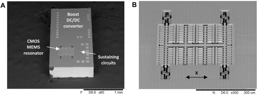
FIGURE 8. (A) BCD MEMS chip with a micromechanical resonator, (B) Magnified SEM image of the micromechanical resonator (Tseng et al., 2015).
The Design Flow of TSRI’s CMOS MEMS Platform
Figure 9 shows the CMOS MEMS design flowchart provided by TSRI. Since the process of the front-end CMOS platform is the same, the process design kits (PDKs) of circuit design environment, simulation, and verification steps provided by the foundry can use the existing design flow, including the device parameters and models for full-custom, cell-based, and radio frequency (RF) ICs. For MEMS, the foundry currently does not provide corresponding PDK. Academic researchers can use the computer-assisted design (CAD) environment provided by TSRI to design the two-dimensional (2D) mask layout of the microstructure, where the 2D mask layer is the thin film layer defined in the CMOS process. After completing the 2D layout, the CMOS process flow kit provided by TSRI can be used with the preprocessing module of finite element method (FEM) software to create a 3D model. The sensor is usually designed using FEM software for multiphysics characteristic analysis. At this stage, the stress gradient effect can also be incorporated, which can more accurately simulate the characteristics of the actual sensor device. After simulating the sensor and readout circuit, respectively, it is recommended to use the CAD tool provided by the CMOS foundry for overall cosimulation to calculate the parasitic effects of the integrated layout and ensure the functionality of the circuit signal. The sensor characteristics can be described by Verilog-A syntax, or the signal change of the sensor can be substituted by the model of the circuit lump element. Based on the verification procedure developed for decades using the CMOS process, integration verification of the sensor and circuit can also be debugged using relevant functions in the CAD tool. For example, the confirmation of electrical signal connection can be specified in the software to confirm whether the signal is connected across the sensor and a specific metal layer of the circuit, thereby preventing open-circuit signal errors in the process. The foundry also provides parametric models for layout parasitic extraction and post-layout simulation, which can extract and correct the effects of coupling capacitance and series resistance between circuits and metal routing, preventing attenuating circuit and sensor characteristics. After passing a complete DRC and post-layout extraction verification, the simulation characteristics and manufacturing procedures of the CMOS MEMS wafer can be confirmed, and the wafer can be produced in the foundry.
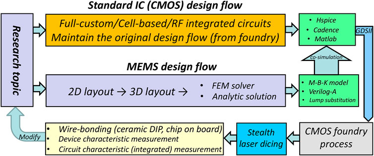
FIGURE 9. CMOS MEMS design flowchart provided by TSRI.
Table 1 summarizes the foundry-oriented (CMOS) platforms that have been published in the literature in recent years. Some of these processes can provide foundry services through IC service organizations such as TSRI, MOSIS, CMC, and Europractice. TSRI has provided CMOS MEMS service platform for 19 years (since 2003). Taiwanese academia uses TSRI’s design service platform to perform wafer-level UMC’s 0.18 µm CMOS MEMS process or TSMC’s 0.35 µm with APM’s post-CMOS micromachining process. As shown in Figure 10, over the past 3 years, Taiwanese academic customers developed at least 130 chip designs per year, which can be successfully validated, tape out, and fabricated. Related fields include physical sensors and actuators, RF MEMS, ultrasonic sensors, biomedical integrated sensor chips, optical mirrors, and optoelectronic integrated sensor chips, etc.
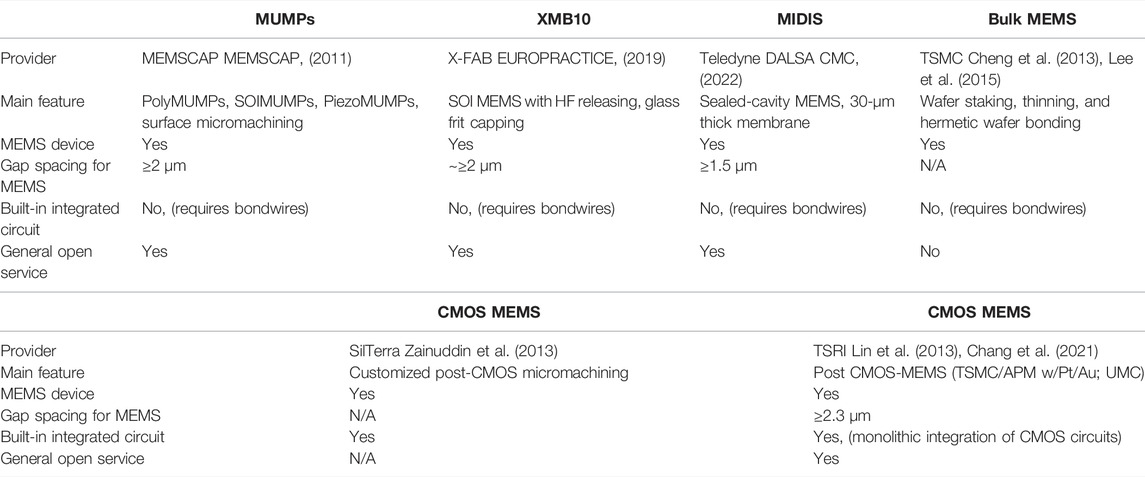
TABLE 1. Comparison of published foundry-oriented (CMOS) MEMS Platforms.
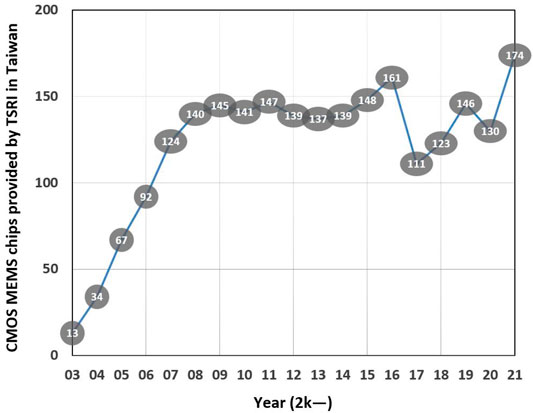
FIGURE 10. Statistics of CMOS MEMS chips provided by TSRI for academic customers in Taiwan.
Conclusion
Manufacturing of CMOS integrated sensors can benefit from the low production cost of CMOS process, stable manufacturing cycles, reliable yields, direct integration with circuits, and access to numerous already developed and proven circuit IPs. Through the development and improvement of CMOS MEMS technology, some sensor chips can be realized using fabless business model even if they do not have the process technology and integrated manufacturing capabilities of their own foundries. With the increase of CMOS process technology modules and more complex functions of chips, integrated development of CMOS MEMS ICs has good prospects.
Author Contributions
The author confirms being the sole contributor of this work and has approved it for publication.
Conflict of Interest
The author declares that the research was conducted in the absence of any commercial or financial relationships that could be construed as a potential conflict of interest.
Publisher’s Note
All claims expressed in this article are solely those of the authors and do not necessarily represent those of their affiliated organizations, or those of the publisher, the editors and the reviewers. Any product that may be evaluated in this article, or claim that may be made by its manufacturer, is not guaranteed or endorsed by the publisher.
References
Chang, C. Y., Tseng, S. H., Chiang, M. H., Hsin, C. T., Ke, L. Y., Wang, Y. J., et al. (2021). “CMOS-MEMS Multi-Sensor Single Chip with High Heat Dissipation and Low-Temperature Hermetic Sealing,” in Proceedings of the IEEE Int. Electron Devices Meeting (IEDM), San Francisco, CA, USA, December 2021. doi:10.1109/iedm19574.2021.9720536
Cheng, C. W., Liang, K. C., Chu, C. H., Horsley, D. A., and Fang, W. (2013). “Single Chip Process for Sensors Implementation, Integration, and Condition Monitoring,” in Proceedings of the IEEE 2013 Transducers & Eurosensors XXVII: The 17th International Conference on Solid-State Sensors, Actuators and Microsystems (TRANSDUCERS & EUROSENSORS XXVII), Barcelona, Spain, June 2013, 730–733.
Chiu, Y., Hong, H.-C., and Wu, P.-C. (2013). Development and Characterization of a CMOS-MEMS Accelerometer with Differential LC-Tank Oscillators. J. Microelectromech. Syst. 22 (6), 1285–1295. doi:10.1109/jmems.2013.2282419
Chiu, Y., Huang, T. C., and Hong, H. C. (2014). A Three-axis Single-Proof-Mass CMOS-MEMS Piezoresistive Accelerometer with Frequency Output. Sensors Mater. 26, 95–108.
CMC (2022). Teledyne DALSA MIDIS Platform. Available at: https://www.cmc.ca/teledyne-dalsa-midis-platform/.
Dai, C.-L., Xiao, F.-Y., Juang, Y.-Z., and Chiu, C.-F. (2005). An Approach to Fabricating Microstructures that Incorporate Circuits Using a post-CMOS Process. J. Micromech. Microeng. 15, 98–103. doi:10.1088/0960-1317/15/1/015
Drienhuizen, B. P. V., Goosen, J. F. L., French, P. J., and Wolffenbuttel, R. F. (1993). Comparison of Techniques for Measuring Both Compressive and Tensile Stress in Thin Films. Sensors and Actuators A 37-38, 756–765. doi:10.1016/0924-4247(93)80128-4
EUROPRACTICE (2019). X-fab. Available at: https://europractice-ic.com/technologies/mems/x-fab/.
Luo, H., Zhang, G., Carley, L. R., and Fedder, G. K. (2002). A post-CMOS Micromachined Lateral Accelerometer. J. Microelectromech. Syst. 11, 188–195. doi:10.1109/jmems.2002.1007397
Hsieh, K.-Y., Chiu, J., and Lu, M. S.-C. (2020). Development of CMOS Micromachined Capacitive Squeeze-Film Pressure Sensors. IEEE Sensors J. 20, 9698–9705. doi:10.1109/jsen.2020.2990187
Kumagai, M., Sakamoto, T., and Ohmura, E. (2007). “Laser Processing of Doped Silicon Wafer by the Stealth Dicing,” in Proceedings of the 2007 International Symposium on Semiconductor Manufacturing, Santa Clara, CA, USA, October 2007, 521–524.
Lee, F. Y., Liang, K. C., Cheng, E., and Fang, W. (2015). “Design and Implementation of a Fully-Decoupled Tuning fork (FDTF) MEMS Vibratory Gyroscope for Robustness Improvement,” in Proceedings of the IEEE 2015 Transducers - 2015 18th International Conference on Solid-State Sensors, Actuators and Microsystems (TRANSDUCERS), Anchorage, AK, USA, June 2015, 1160–1163.
Liao, P. L., Wang, P. H., Li, M. L., and Lu, S. C. (2013). “A CMOS MEMS Capacitive Ultrasonic Sensor Array for Three-Dimensional Photoacoustic Imaging,” in Proceedings of the 2013 IEEE 26th International Conference on Micro Electro Mechanical Systems (MEMS), Taipei, Taiwan, January 2013, 613–616. doi:10.1109/memsys.2013.6474316
Lin, M. J., Lan, B. C., Wang, M. I., and Huang, C. H. (2013). Method for Fabricating Integrated Circuit. US Patent, US20130023081A1.
Liu, J.-C., Hsiung, Y.-S., and Lu, M. S.-C. (2012). A CMOS Micromachined Capacitive Sensor Array for Fingerprint Detection. IEEE Sensors J. 12, 1004–1010. doi:10.1109/jsen.2011.2167748
MEMSCAP (2011). MUMPs. Available at: http://www.memscap.com/products/mumps.
Offenberg, M., Larmer, F., Elsner, B., Munzel, H., and Riethmuller, W. (1995). “Novel Process for a Monolithic Integrated Accelerometer,” in IProceedings of the International Solid-State Sensors and Actuators Conference - TRANSDUCERS '95, Stockholm, Sweden, June 1995, 589–592.
Sherman, S. J., Tsang, W. K., Core, T. A., Payne, R. S., Quinn, D. E., Chau, K. H.-L., et al. (1992). “A Low Cost Monolithic Accelerometer Product/technology Update,” in Proceedings 1992 International Technical Digest on Electron Devices Meeting (IEDM), San Francisco, CA, USA, December 1992, 501–504.
Smith, J. H., Montague, S., Sniegowski, J. J., Murray, J. R., and McWhorter, P. J. (1995). “Embedded Micromechanical Devices for the Monolithic Integration of MEMS with CMOS,” in Proceedings of the IEEE International Electron Devices Meeting (IEDM), Washington, DC, USA, December 1995, 609–612.
Sun, C. M., Tsai, M. H., and Fang, W. (2009). “Design and Implementation of a Novel CMOS-MEMS Single Proof-Mass Tri-axis Accelerometer,” in Proceedings of the 2009 IEEE 22nd International Conference on Micro Electro Mechanical Systems, Sorrento, Italy, January 2009, 809–812. doi:10.1109/memsys.2009.4805506
Tsai, H.-H., Lin, C.-F., Juang, Y.-Z., Wang, I.-L., Lin, Y.-C., Wang, R.-L., et al. (2010). Multiple Type Biosensors Fabricated Using the CMOS BioMEMS Platform. Sensors Actuators B: Chem. 144, 407–412. doi:10.1016/j.snb.2009.01.061
Tseng, S.-H., Hung, Y.-J., Juang, Y.-Z., and Lu, M. S.-C. (2007). A 5.8-Ghz VCO with CMOS-Compatible MEMS Inductors. Sensors Actuators A: Phys. 139, 187–193. doi:10.1016/j.sna.2006.12.014
Tseng, S.-H., Lu, M. S.-C., Hung, Y.-J., and Juang, Y.-Z. (2010). High-Q CMOS MEMS Resonator Oscillator Fabricated in a MPW Batch Process. Proced. Eng. 5, 1360–1363. doi:10.1016/j.proeng.2010.09.367
Tseng, S.-H., Lu, M. S.-C., Wu, P.-C., Teng, Y.-C., Tsai, H.-H., and Juang, Y.-Z. (2012). Implementation of a Monolithic Capacitive Accelerometer in a Wafer-Level 0.18 Μm CMOS MEMS Process. J. Micromech. Microeng. 22, 055010. doi:10.1088/0960-1317/22/5/055010
Tseng, S. H., Fang, C. L., Wu, P. C., Juang, Y. Z., and Lu, M. S. C. (2008). “A CMOS MEMS thermal Sensor with High Frequency Output,” in Proceedings of the IEEE Sensors, Lecce, Italy, October 2008, 387–390. doi:10.1109/icsens.2008.4716460
Tseng, S. H., Hsieh, Y. T., Lin, C. C., Tsai, H. H., and Juang, Y. Z. (2015). “CMOS MEMS Resonator Oscillator with an On-Chip Boost DC/DC Converter,” in Proceedings of the IEEE Conf. Solid-State Sensors, Actuators and Microsystems (TRANSDUCERS), Anchorage, AK, USA, June 2015. doi:10.1109/transducers.2015.7181342
Xie, H., and Fedder, G. K. (2000). “A CMOS Z-axis Capacitive Accelerometer with Comb-finger Sensing,” in Proceedings IEEE Thirteenth Annual International Conference on Micro Electro Mechanical Systems (Cat. No.00CH36308), Miyazaki, Japan, January 2000, 496–501.
Keywords: CMOS MEMS, design platform, accelerometer, post-CMOS, single-chip
Citation: Tseng S-H (2022) CMOS MEMS Design and Fabrication Platform. Front. Mech. Eng 8:894484. doi: 10.3389/fmech.2022.894484
Received: 11 March 2022; Accepted: 04 April 2022;
Published: 26 April 2022.
Edited by:
Sheng-Shian Li, National Tsing Hua University, TaiwanReviewed by:
Yi Chiu, National Yang Ming Chiao Tung University, TaiwanChingfu Tsou, Feng Chia University, Taiwan
Copyright © 2022 Tseng. This is an open-access article distributed under the terms of the Creative Commons Attribution License (CC BY). The use, distribution or reproduction in other forums is permitted, provided the original author(s) and the copyright owner(s) are credited and that the original publication in this journal is cited, in accordance with accepted academic practice. No use, distribution or reproduction is permitted which does not comply with these terms.
*Correspondence: Sheng-Hsiang Tseng, shtseng@narlabs.org.tw