A simple flash and freeze system for cryogenic time-resolved electron microscopy
 Biddut Bhattacharjee
 Md Mahfuzur Rahman2†
  Michael H. B. Stowell
- 1University of Colorado Boulder, Boulder, United States
- 2University of Texas Southwestern Medical Center, Dallas, United States
As the resolution revolution in CryoEM expands to encompass all manner of macromolecular complexes, an important new frontier is the implementation of cryogenic time resolved EM (cryoTREM). Biological macromolecular complexes are dynamic systems that undergo conformational changes on timescales from microseconds to minutes. Understanding the dynamic nature of biological changes is critical to understanding function. To realize the full potential of CryoEM, time resolved methods will be integral in coupling static structures to dynamic functions. Here, we present an LED-based photo-flash system as a core part of the sample preparation phase in CryoTREM. The plug-and-play system has a wide range of operational parameters, is low cost and ensures uniform irradiation and minimal heating of the sample prior to plunge freezing. The complete design including electronics and optics, manufacturing, control strategies and operating procedures are discussed for the Thermo Scientific™ Vitrobot and Leica™ EM GP2 plunge freezers. Possible adverse heating effects on the biological sample are also addressed through theoretical as well as experimental studies.
Introduction
Macromolecular complexes are flexible dynamic systems that undergo a myriad of structural changes in response to all manner of perturbations. The kinetics and magnitudes of these structural changes cover a broad range from picoseconds to years and bond-vibrations to protein aggregation and plaque formation Figure 1. The structural investigation of intermediate states provides crucial information for mapping the reaction coordinates of biological systems and helps to elucidate mechanisms of action. Accessing such intermediate states has historically been achieved using pharmacological agents and/or site-specific mutagenesis to “trap” intermediates states. These methods have provided important insight into many biological systems, e.g., the use of non-hydrolysable ATP analogs to trap ATPases in the apparent transition state. The use of active site mutants has similarly expanded our knowledge of intermediate states of various enzymes and molecular machines. Non-etheless, many biological complexes are not amenable to such methods or multiple intermediate states exist that cannot be readily trapped through chemical or mutational means. Additionally, the ability to directly determine native intermediate structural states in the absence of mutagenesis and or inhibitor trapping would provide more rigorous and reliable data for mapping structural transitions. Substantial efforts have pursued the use of ultrafast X-ray lasers to study charge separation in photosystems (Kupitz et al., 2014) and the use of Laue methods in time-resolved X-ray crystallographic studies has a long and storied history (Moffat, 2019). Such methods are suitable for very rapid processes (<1 ns), with minor conformational changes that are not expected to be affected by crystal contacts. Conversely, cryoEM is ideally suited for studying large conformational changes on the timescale of milliseconds to minutes. Furthermore, as modern computational approaches in cryoEM can 3D classify particles, branched conformational change pathways can be quantified and resolved. While the practical lower limit of 1 ms is governed by the cooling rate of the plunge freezing method (Dubochet, 2007; Frank, 2017), in-situ rapid heating and cooling methods may provide access to microsecond timescales (Voss et al., 2021; Bongiovanni et al., 2022).
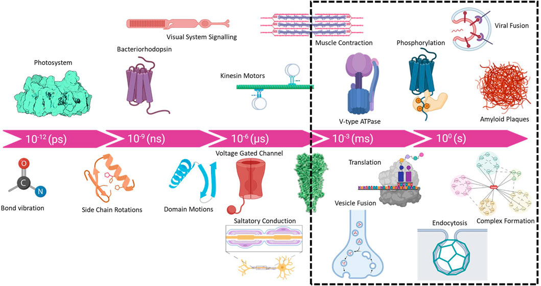
FIGURE 1. Timescale of biological processes from bond vibrations and charge separation (femto and pico second) to complex assembly (minutes to hours) and even amyloid plaque formation in the human brain (years). Although new methods are being developed, the practical range for cryoTREM is limited by the rate of sample cooling which is ∼10,000 K/s and places a lower limit of ∼1 ms due to the cooling rate using traditional plunge freezing instruments.
Time-resolved studies have been at the heart of fundamental understandings of many biological complexes including enzymes, channels, photosystems, and molecular motors. Early efforts in cryoTREM began with a series of foundational studies on the nicotinic acetylcholine receptor using a spraying method to capture the open state of the acetylcholine receptor (Berriman and Unwin, 1994; Unwin, 1995). Helical crystal samples were sprayed just prior to plunge freezing in liquid ethane to capture the open state of the receptor and included ferritin particles as fiducials to identify regions where droplets had mixed with the sample. Subsequent efforts by several groups have adopted similar strategies using a variety of similar methods including on the fly droplet mixing and pre spray microfluidic mixing (White et al., 2003; 1998; Lu et al., 2014; Chen et al., 2015; Feng et al., 2017; Kaledhonkar et al., 2018; Fu et al., 2019; Dandey et al., 2020). The main disadvantages of the system are the requirement for specialized equipment and most importantly the control of the liquid film thickness prior to plunge-freezing. Film thickness in particular is critical factor in obtaining quality data and is routinely measured during data collection (Rice et al., 2018). This ensures that the film is thin enough for rapid cooling but not too thin as to damage particles due to the air-water interface.
Alternatively, the use of light to trigger biological activity is well-established in the field of rapid enzyme kinetics and was first successfully implemented in cryoEM to investigate conformational changes in bacteriorhodopsin (Subramaniam et al., 1999; Subramaniam et al., 1993; Subramaniam and Henderson, 1999) and an automated device for flash-photolysis and flash-freezing was subsequently described (Shaikh et al., 2009). Despite these early successes and developments in the use of light activation for cryoTREM this approach has not seen substantial adoption. This is surprising considering the many advances in the development of caged compounds and optogenetic tools which have been implemented with great success in many fields many of which have become commercial products (Tischer and Weiner, 2014; Ferenczi et al., 2019; Ellis-Davies, 2020; Monteiro et al., 2021). One of the major concerns with the use of light for cryoTREM is the potential for thermal heating of the sample due to absorption by both the sample and the EM grid. Several early studies suggested that such heating would preclude the use of light for all but the most quantum efficient systems such as bacteriorhodopsin (Siegel et al., 1994; Shaikh et al., 2009). However, these studies utilized broad band light sources and temperature measurement methods that did not control for the photoelectric effect. In fact, recent work has demonstrated minimal apparent heating in plunge frozen samples irradiated with a narrow band high-power LED (Yoder et al., 2020).
Here we provide detailed analysis of the potential use of light as a trigger for cryoTREM systems. Using both theoretical and experimental studies, we determine the optimal parameters for a light triggered cryoTREM system employing low-cost LED light sources suitable for exploiting a wide range of readily available caged compounds and optogenetic tools. These data were then used to guide the design, building, and testing of a low-cost LED light source suitable for plug and play into the two most widely used automated plunge-freezers, the Thermo Scientific Vitrobot Mark IV and the Leica EM GP2. We provide a comprehensive analysis of light absorption and thermal heating of copper and gold EM grids and measure temperature jumps for several wavelengths and irradiation times on the order of milliseconds. A description of the components is provided so that others can readily construct such instrumentation for future cryoTREM studies.
Results
The success in light activated uncaging of compounds to capture the desired intermediate states of samples of interest will depend on many factors. The required irradiation power is one of the basic factors that must be known or estimated. Table 1 lists the calculated power requirement for some commonly available caged compounds and photoactive proteins. For these calculations we assumed an exposure of 20 milliseconds, 100 nm liquid depth after blotting, the concentration of the caged compound 10 mM, and the desired concentration of the released product 200 µM.
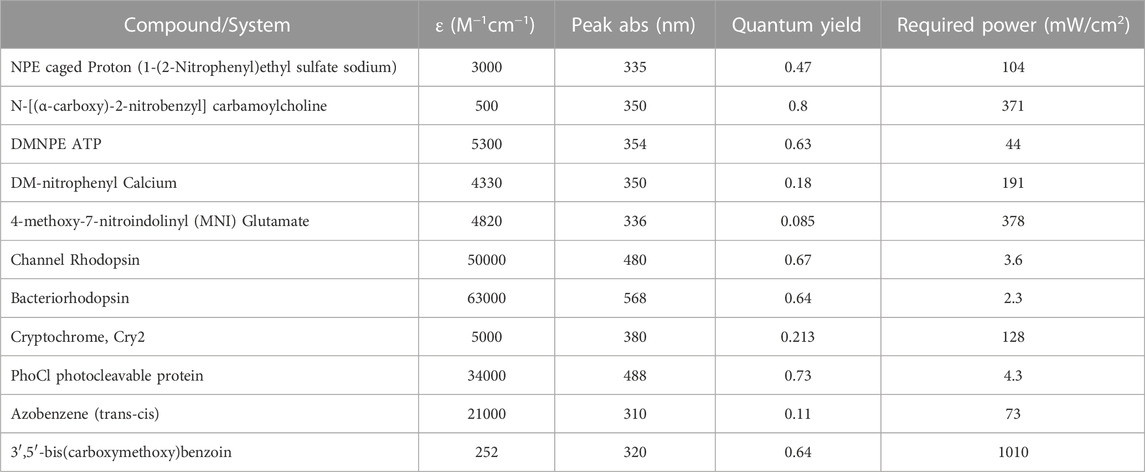
TABLE 1. Exemplary photoactive compounds/proteins and associated photophysical properties.
One of the major concerns in the light activation of caged compounds or optogenetics samples on a copper or gold grid is the thermal effects due to radiation absorption. The absorption coefficient (optical depth, α) of water in the 300–700 nm range is between 0.01 m−1 and 0.1 m−1. Considering the typical aqueous layer thickness of 100 nm after blotting, the temperature rise due to a 1 W/cm2 beam of 365 nm radiation for 1 s is estimated to be 0.0034°C (
The system we report here is designed for light sources of wavelengths 365 nm and 455 nm. The following discussion will be based on 365 nm radiation. Due to the finite conductivity of a given metal, the incident electromagnetic wave is attenuated to zero intensity within a certain distance from the surface. This distance is characterized by the ‘skin/penetration depth’ or ‘attenuation depth’ given by
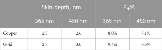
TABLE 2. Skin depth penetration calculations.
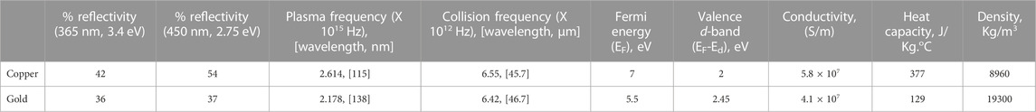
TABLE 3. Finite conductivities of copper and gold.
The above simplified models are based on very high electrical conductivities, i.e.,
The free-electron theory of metals attempts to explain the behavior of metals when the EM wave frequency is much greater than the collision frequency, i.e., the near-infrared and visible spectra. Due to the higher frequencies, electrons in metal are collectively treated as a plasma gas, and the behavior of metals are characterized by the plasma frequency. This frequency is defined as,
The electronic band structure of noble metals helps greatly to understand the optical behavior. Copper and gold have bound electrons in the completely filled valence d-bands (3d and 5d) below the Fermi energy (EF) level. Electrons in the s-band can be continuously excited by low frequency EM waves. However, electrons in the d-band can be excited above EF when photons of frequency
The wave number or the propagation constant in metals is given by
The rise in temperature can be estimated from the properties of the grid and the irradiance of the exciting source. The dissipative power per unit area as a fraction of the total irradiance is given by:
where
To complement these theoretical studies, we constructed a thermal test bed for both copper and gold grids that can provide a direct experimental measurement of temperature rise due to irradiation. The system is comprised of a liquid light guided LED, coupled to an aspheric lens to provide uniform beam output, Figures 2A, B. The use of an aspheric lens to achieve beam uniformity is critical for both these measurements as well as future implementation in cryoTREM to ensure that all regions of the sample are activated equally and minimizes off axis translation variation in beam intensity as occurs with a typical focusing lens (Yoder et al., 2020). Using this test bed, we measured the temperature rise as a function of time for a 2 W/cm2 365 LED beam, Figure 2C. The data demonstrate a minimal temperature rise for the targeted power density and irradiation time with nominal variation between grid types and excellent agreement with the above theoretical analysis.
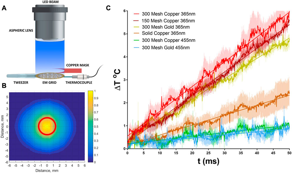
FIGURE 2. Measurement of thermal heating by UV (365 nm) and Visible (455 nm) LED beam. (A) Experimental setup that replicates the experimental conditions within the Vitrobot during light triggering, see methods. (B) Measured beam profile demonstrating the beam uniformity within the EM grid diameter (red circle). 2D intensity profile was constructed from a series of signals measured by a linear photodiode array, see methods. (C) Temperature rise curves during irradiation for several grid types typically used in cryoEM at both 365 and 455 nm. Data are averages of 3 separate measurements using the measurement setup in A and errors are shown as shaded color.
Both copper and gold are excellent conductors of heat, and the thermal diffusivities are ∼118 × 106 μm2/s and ∼126 × 106 μm2/s respectively. For grids of thicknesses 25 μm, the estimated timescale for the temperature gradient between the top and the bottom surfaces to subside are in microseconds. Hence, the readings from the thermocouple from the bottom surface are expected to be accurate representation of the instantaneous bulk temperature of the grid. Figure 2 shows the temperature rise of different types of grid when subject to the 365 nm light beam. The grid temperature increases linearly with time due to the absence of any significant heat loss during the early stage of irradiation. However, this rise in temperature slows down after about 80 ms (data not shown) mainly due to heat transfer to the tweezer.
The reliability of temperature data can be compared to the theoretical values applying the fundamental relation
It is noted that the surface quality of metals affects light absorption considerably (Gevorkian et al., 2022). We used commercially available grids without any surface modification and the deviation of the estimated absorptivity calculated from the measured temperature rise versus the published values might be due to the presence of rough peaks and valleys, the non-polarized character of the beam, and the mesh structure. The measured temperature rise per unit of irradiation energy for gold grids is 0.86°C/mJ. This is less than the theoretical value relative to that of copper grids as found from
In summary, the measured temperature rise of grids in our system is well within the theoretical limit, and reasonably close to the published absorptivity values for mirror finish metal thin films. However, we want to emphasize here that the photothermal heating of grids is significantly overestimated in some publications (Siegel et al., 1994; Shaikh et al., 2009). Siegel et al. (1994) reported a temperature rise of 51°C in 1 ms in a copper grid subject to a Xenon flashtub. This corresponds to about 430 W/cm2 light power incident on the grid and fully absorbed. While it is possible to generate and apply this level of power, a lower irradiance is preferred to avoid any undesired biological activity. Surprisingly, these early studies using a xenon lamp-based flash system reports grid temperature rises of ∼43°C in 5 ms, which translates to ∼3.2°C/mJ after taking the applied power into account (Shaikh et al., 2009). This value is almost twice the theoretical limit of 1.67°C/mJ. These previously reported temperature rises due to irradiation are overestimations originating from the measurement methods. In both studies, wires of copper and copper-nickel alloy were either woven into or spot-welded onto copper grids. Nickel absorbs all frequencies of radiation since it has a partially occupied d-band. Therefore, exposing the thermocouple joints to strong radiation, particularly in the 350–400 nm range, results in a photoelectric effects that gives rise to a spurious response of the thermocouple.
Conclusion
Here we have combined theoretical and experimental studies to demonstrate that light activated cryoTREM is feasible with nominal heating of the sample due to EM grid absorption. Importantly, the theoretical and experimental results reported here are in excellent agreement and allay thermal heating concerns raised by prior studies when activating a wide variety of photoactivatable compounds and biological species. We have designed and implemented two plug and play light activated systems for both the Vitrobot Mark IV and the Leica EM GP2 that provide capabilities for light activated cryoTREM studies in the millisecond to minute regime suitable for a wide range of investigations. The complete component list for assembling both systems is provided in order to allow other investigators to assemble similar systems at low cost. The results presented should enable other investigators to readily implement cryoTREM within the standard workflow of cryoEM.
Methods
Theoretical consideration of heating. The penetration depth for various metals and energies was calculated using a uniform x-polarized plane wave
where
where
The continuity of tangential components of electric fields at the surface yields
where
In the absence of a pure surface current, the tangential components of the magnetic fields are continuous
However, the incident wave induces current
where
Here
in Eq. 6 we get
The reflectivity is given by
The dielectric function for metal in the optical frequency range is given by
where
The complex wavenumber is given by
We observe that the complex conductivity is a function of frequency and various dielectric components. The overall effect is a combination of the dissipative (real) part, different from the DC conductivity value, and the reactive (imaginary) part. For copper at 365 nm, the conductivity is
Power calculations for Table 1. Assuming that the non-linear effects due the absorption of photoproducts are negligible during the early short period of the reaction, the required power that the source must deliver at the grid can be calculated by the following:
where P is the required power at the grid, W/cm2, C is the speed of light (m/s), h is Plancks constant (J.s), N is Avogadro’s number, V is the liquid volume (L), cp is the desired photo product concentration (M), λ is the excitation wavelength (m), t is the exposure time (s), φ is the quantum yield of the photoreaction, ε is molar absorptivity (M-1cm-1), c is the starting material concentration (M), L is the absorption path length or liquid depth (m) and Al is the liquid surface area (cm2). Assuming that the light delivery system is installed so that the sample side of the grid is illuminated, the area of light absorption is 0.07068 cm2, and the liquid depth is 100 × 10–7 cm and the volume of liquid is 7.07 × 10⁻¹⁰ L.
Integrated controller design. The operation of the light trigger system is controlled by an ATMEGA 328P based microcontroller board (Arduino Nano). This board is programmed to receive some basic parameters from the user and execute the timed signal generation for turning the LED on and off. The board is connected to a 2.8” 320 × 240 pixel touch screen to interact with the user as well as to get basic commands and parameters. Two-way communication between the microcontroller and the display is accomplished through serial peripheral interface (SPI) protocol. The microcontroller sends appropriate command signals to the digital-to-analog converter to generate timed voltage for the LED driver. This voltage is proportional to the LED output power. The LED driver channels a relatively high driving voltage of 24 V to the LED. To synchronize the LED activation with the procedures in Vitrobot a signal from the foot pedal is directed to one of the input ports of the microcontroller. The specific input port is interrupt capable so that the dependent processor operations are done in a precisely timed manner. An example scenario could be turning the LED on after a user supplied delay which may be roughly the blotting time. The controller starts a timer as soon as the user presses the foot pedal to start blotting. After the specified delay has been completed, the controller sends signals for LED activation. This design of open input ports with interrupt capabilities is quite simple yet universal in that synchronous signals from any time-point within the sample preparation as well as any other kind of sensor can be integrated to this system. This makes the controller suitable for installing onto other vitrification instruments with ease. In the Vitrobot application the exposure time was determined to be 17 ms and the delay between exposure and liquid ethane bath was 54 ms. The implementation on the Leica EM GP2 system provides longer exposure times and variable delays.
Beam profile determination. The output beam profile was characterized using a linear photodiode array (TSL1406, AMS-OSRAM AG). This device has 768 photodiodes each of 63.5 µm by 55.5 µm. The sensitivity of each pixel at 365 nm is 11.25 V/(µJ/cm2), and minimum integration time is 66 µs. It is noted that a good sensitivity in the UV range is critical for selecting the sensor in beam profile measurement. We found the sensitivity to be more than enough so that we had to use a combination of neutral density filters to prevent pixel saturation even when the LED was driven by current near the threshold value. The sensor was mounted on a linear stage having a translational resolution of 10 µm. Since in our system the approximate beam diameter beyond the condenser lens is 16 mm, there were a maximum of 252 pixels covered by the UV beam. This implies that there were enough pixels to capture a smooth intensity variation along the sensor array. The liquid light-guide (LLG) and lens assembly was kept at a fixed position with respect to the laboratory coordinate system and was aligned so that the beam center is overlapped with the central segment of the sensor array. Pixel data were acquired by a high-speed microcontroller (Teensy 3.6 Board, 180 MHz) through analog ports, and subsequently transferred to the host desktop computer through USB connection. Beam intensity was recorded by aligning the pixel array along the center of the beam and subsequent intensities were collected by translating the linear stage, along with the sensor, by a known distance in the direction perpendicular to the pixel array. Pixel data were post-processed by correcting for the flat-field as well as by normalizing the intensities to provide the two dimensional intensity profile of the beam and the contour map. The intensity profile closely resembles that of a Gaussian beam and moreover, the central area of 2-mm diameter corresponding to the effective EM-grid area contains the dominant uniform intensity. The intensity within this area varies from 80% of the maximum value near the periphery to 100% at the central irradiation zone.
Grid exposure timing measurement. Grid exposure times and energy deposition were determined using a hall sensor First, we measured the beam diameter (dB) projected on a plane orthogonal to the radiation propagation and containing straight line of grid travel. The goal was to determine the time the freely falling grid takes to pass this distance provided the path segment is vertically positioned exactly where the beam is located. We used two small magnets (1.59 mm × 1.59 mm × 1.59 mm Neodymium, B111 K&J Magnetics) and a hall-effect latch sensor (DRV5011, Texas Instruments Inc.) to get the timing signals. We configured the setup where the two magnets were mounted on the tweezers. One at the tip of the tweezer and the other separated by a distance of dB corresponding to the grid beam diameter. The hall sensor was mounted on the fixed supporting rod extending beyond the chamber through the sample loading port. The sensor was fixed at the upper most position of the UV beam. As the plunger falls after the blotting operation, the hall sensor output signal changes levels (high: 5 V, low: 0 V) twice due to the two magnets. These changes were captured using an oscilloscope. Since the typical response time of the sensor is 13 µs, this method results in an accurate estimate of the grid exposure duration of 17 ms while falling toward liquid ethane. It is noted that this exposure time can also be calculated from the fundamental equations of Newtonian mechanics considering free fall under gravity.
Optical Train Design. Components for the Vitrobot and GP2 are listed in Table 4. The high-power UV LED (LZ4-V4UV0R-0000, 5.7 W, Osram Sylvania Inc.) is mounted on a metal core printed circuit board (MCPCB) which in turn is mounted on a heatsink. We mounted the LED on the heatsink for the ease of assembly. But the heatsink also provides an additional safety in case of prolonged LED operation. The input end of the liquid-light guide is carefully assembled with the LED-heat sink part such that the core of the light guide is centered with that of the LED. In addition, the distance of the light guide from the LED surface is minimized to ensure maximum collection of light into the guide. The output end of the light guide is connected to a condenser lens housing, and positioned with respect to the lens so achieve nearly a collimated beam. This lens housing is installed inside the climate chamber of Vitrobot Mark IV, and the lens axis aligns with the center of the grid at the blotting position. For the Leica EM GP2 system, the blotting position of the grid is not at the same vertical position as the sample loading port, which is true in Vitrobot Mark IV system (Figure 3). We designed special adapter assembly for the GP2 system so that the output light beam aims at the grid. The assembly consists of a 3D printed part, a kinematic pitch/yaw adapter and an aspheric condenser lens. The kinematic adapter is used to fine tune the beam direction to correct for any misalignment originating from the inaccuracies of part dimensions and of assemblies. In contrast with the Vitrobot system, where the grid exposure to the light beam is fixed, the GP2 system provides some flexibility in varying the exposure time. This flexibility comes from the fact that the retraction of the blotting arm requires approximately one second before the plunger falls toward the liquid ethane. However, the duration of blotting process may vary depending on the user’s preference and sample type. Light exposure is performed only after the blotting process has been completed to achieve accurate, reproducible and predictable photoproduct concentration. Therefore, the detection of the beginning of blotting process can be utilized to accurately time the light exposure. We designed a wall-mounted photointerrupter based sensor that detects the beginning of the blotting process by sensing the change in the reflected light caused by the blotting arm. The timer in the microcontroller starts after being triggered by the sensor, and the instant of turning the LED on is calculated as follows:
Where
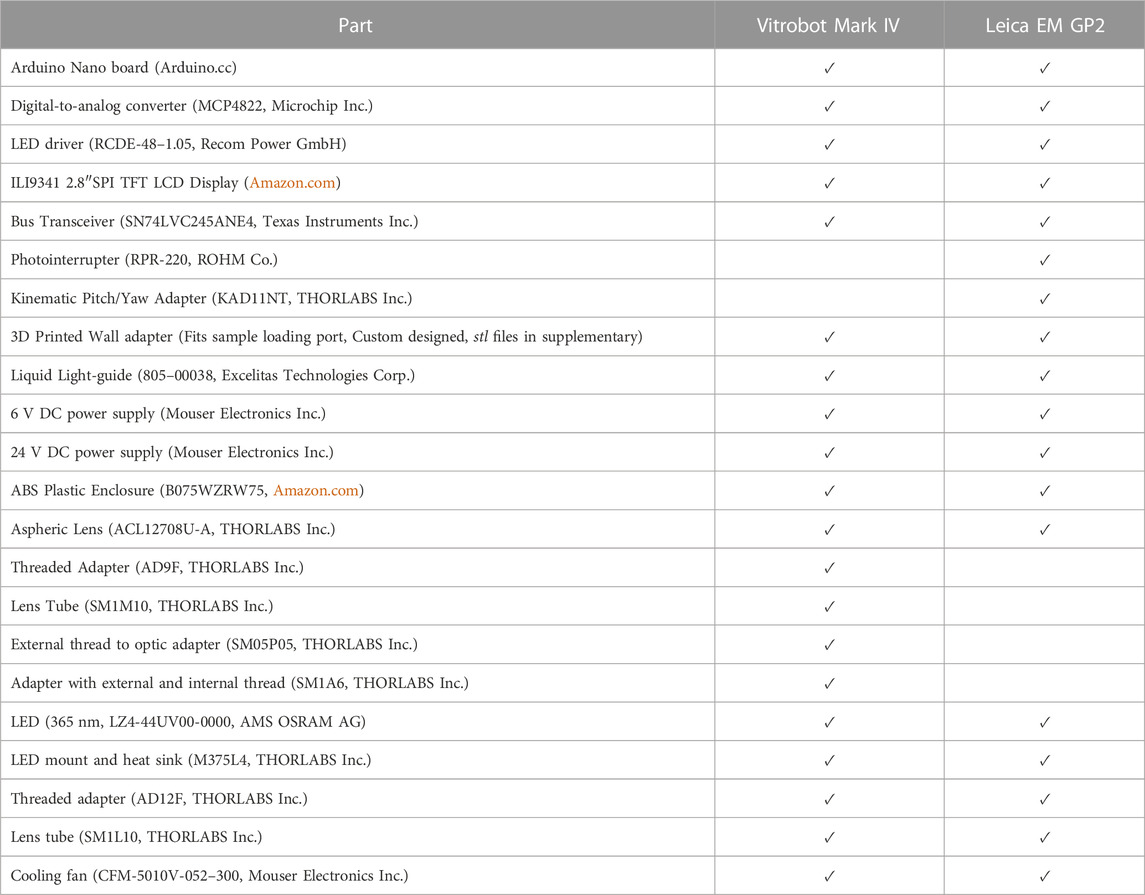
TABLE 4. Optical train components.
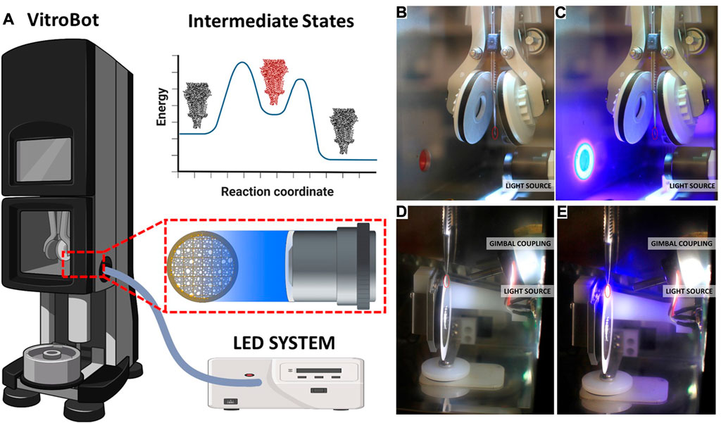
FIGURE 3. LED system with liquid light guide for plug and play cryoTREM. (A) Schematic overview of the system as implemented on the Vitrobot Mark IV, showing the LLG and lens location. A reaction coordinate illustrating the target trapping of an intermediate state (red). (B) Photograph of the Vitrobot environmental chamber with the focusing optics unit installed. (C) Photograph of the Vitrobot environmental chamber with the focusing optics unit installed and the 365 LED light on. (D) Photograph of the GP2 environmental chamber with the focusing optics and gimbal system installed. (E) Photograph of the GP2 environmental chamber with the focusing optics and gimbal system installed and the 365 LED light on. The red circles indicate the location of the EM grid prior to blotting. See Supplemental Material for videos of the system in operation.
Temperature measurements. We used a fine-gage J-type thermocouple (IRCO-001, Omega Engineering Inc.) to measure the temperature change in the grid due to irradiation with 365 nm. The schematic of the experimental setup is shown in Figure 2 and Supplementary Figure S1. There are two major factors in the temperature sensing of the grid that need to be considered. First, the sensor itself must be minimally affected by the radiation. This is related to the mechanism of sensing and/or the arrangement of the sensor. When subject to an intense blue light or UV radiation, the thermocouple typically gives unrealistic readings originating from the photothermal effects. We also experimented with thermopile-based infrared sensor to sense the grid temperature. This type of sensor could not be reliably used due to the absorption of the built in filters, the uncertainty with the emissivity values of grids, and the mismatch between the field-of-view and the grid dimension. The second factor is that the sensor must not thermally load the grid significantly, which is related to the dimensions and hence, the time constant of the sensor. The thermocouple used here is of iron-constantan with approximately 25 micron bead. We mounted the stainless steel tweezer holding the grid on a 3-axis manipulator to adjust the position of the grid relative to the sensor bead. After holding a new grid by the tweezer and mounting on the manipulator, the grid position is lowered such that the bead touches the bottom surface of the rim segment of the grid. Next, the copper mask is positioned so as to minimize the exposure of the thermocouple leads to the light beam. Finally, the output end of the light guide is positioned so that the central portion of the light beam hits the top surface of the grid. Thus, we minimized any spurious reading from the thermocouple by keeping the bead and the leads away from the light beam.
Finite-element simulation. To gain better insight of the grid temperature rise due optical stimulation a finite-element based simulation model was developed in COMSOL Multiphysics. The geometry is developed to represent a 25 µm thick 300-mesh grid held by a stainless-steel tweezer. The model solved the three-dimensional time-dependent heat conduction equation:
where, T is the temperature, αT is the thermal diffusivity,
Data availability statement
The raw data supporting the conclusion of this article will be made available by the authors, without undue reservation.
Author contributions
BB and MS conceived the research studies. BB, MR, RH, and MS designed the experiments. BB and MR performed the experiments. BB and MS wrote the manuscript with contributions from all authors.
Funding
This work was supported in part by grants from the NIH (NS120496 to RH and MS, U24-GM139174 to MS), the MCDB Neurodegenerative Disease Fund to MS and the University of Colorado Open Access Fund for publication costs.
Acknowledgments
We thank our colleagues in MCDB and ME for helpful comments and suggestions and Charlie Bowen for machining services. Some images created with BioRender.com.
Conflict of interest
The authors declare that the research was conducted in the absence of any commercial or financial relationships that could be construed as a potential conflict of interest.
Publisher’s note
All claims expressed in this article are solely those of the authors and do not necessarily represent those of their affiliated organizations, or those of the publisher, the editors and the reviewers. Any product that may be evaluated in this article, or claim that may be made by its manufacturer, is not guaranteed or endorsed by the publisher.
Supplementary material
The Supplementary Material for this article can be found online at: https://www.frontiersin.org/articles/10.3389/fmolb.2023.1129225/full#supplementary-material
References
Axelevitch, A., Gorenstein, B., and Golan, G. (2012). Investigation of optical transmission in thin metal films. Phys. Procedia, 18th Int. Vac. Congr. (IVC-18) 32, 1–13. doi:10.1016/j.phpro.2012.03.510
Babar, S., and Weaver, J. H. (2015). Optical constants of Cu, Ag, and Au revisited. Appl. Opt. 54, 477–481. doi:10.1364/AO.54.000477
Berriman, J., and Unwin, N. (1994). Analysis of transient structures by cryo-microscopy combined with rapid mixing of spray droplets. Ultramicroscopy 56, 241–252. doi:10.1016/0304-3991(94)90012-4
Bongiovanni, G., Harder, O. F., Drabbels, M., and Lorenz, U. J. (2022). Microsecond melting and revitrification of cryo samples with a correlative light-electron microscopy approach. Front. Mol. Biosci. 9, 1044509. doi:10.3389/fmolb.2022.1044509
Chen, B., Kaledhonkar, S., Sun, M., Shen, B., Lu, Z., Barnard, D., et al. (2015). Structural dynamics of ribosome subunit association studied by mixing-spraying time-resolved cryogenic electron microscopy. Struct. Lond. Engl. 23, 1097–1105. doi:10.1016/j.str.2015.04.007
Dandey, V. P., Budell, W. C., Wei, H., Bobe, D., Maruthi, K., Kopylov, M., et al. (2020). Time-resolved cryo-EM using Spotiton. Nat. Methods 17, 897–900. doi:10.1038/s41592-020-0925-6
Dubochet, J. (2007). The physics of rapid cooling and its implications for cryoimmobilization of cells. Methods Cell Biol. 79, 7–21. doi:10.1016/S0091-679X(06)79001-X
Ehrenreich, H., and Philipp, H. R. (1962). Optical properties of Ag and Cu. Phys. Rev. 128, 1622–1629. doi:10.1103/PhysRev.128.1622
Ellis-Davies, G. C. R. (2020). Useful caged compounds for cell physiology. Acc. Chem. Res. 53, 1593–1604. doi:10.1021/acs.accounts.0c00292
Feng, X., Fu, Z., Kaledhonkar, S., Jia, Y., Shah, B., Jin, A., et al. (2017). A fast and effective microfluidic spraying-plunging method for high-resolution single-particle cryo-EM. Struct. Lond. Engl. 1993 25, 663–670.e3. doi:10.1016/j.str.2017.02.005
Ferenczi, E. A., Tan, X., and Huang, C. L.-H. (2019). Principles of optogenetic methods and their application to cardiac experimental systems. Front. Physiol. 10, 1096. doi:10.3389/fphys.2019.01096
Frank, J. (2017). Time-resolved cryo-electron microscopy: Recent progress. J. Struct. Biol. 200, 303–306. doi:10.1016/j.jsb.2017.06.005
Fu, Z., Indrisiunaite, G., Kaledhonkar, S., Shah, B., Sun, M., Chen, B., et al. (2019). The structural basis for release-factor activation during translation termination revealed by time-resolved cryogenic electron microscopy. Nat. Commun. 10, 2579. doi:10.1038/s41467-019-10608-z
Gevorkian, Z. S., Petrosyan, L. S., and Shahbazyan, T. V. (2022). Light absorption by weakly rough metal surfaces. Phys. Rev. B 106, 205302. doi:10.1103/PhysRevB.106.205302
Johnson, P. B., and Christy, R. W. (1972). Optical constants of the noble metals. Phys. Rev. B 6, 4370–4379. doi:10.1103/PhysRevB.6.4370
Kaledhonkar, S., Fu, Z., White, H., and Frank, J. (2018). Time-resolved cryo-electron microscopy using a microfluidic chip. Methods Mol. Biol. Clifton N. J. 1764, 59–71. doi:10.1007/978-1-4939-7759-8_4
Kupitz, C., Basu, S., Grotjohann, I., Fromme, R., Zatsepin, N. A., Rendek, K. N., et al. (2014). Serial time-resolved crystallography of photosystem II using a femtosecond X-ray laser. Nature 513, 261–265. doi:10.1038/nature13453
Lu, Z., Barnard, D., Shaikh, T. R., Meng, X., Mannella, C. A., Yassin, A., et al. (2014). Gas-assisted annular microsprayer for sample preparation for time-resolved cryo-electron microscopy. J. Micromechanics Microengineering Struct. Devices Syst. 24, 115001. doi:10.1088/0960-1317/24/11/115001
Moffat, K. (2019). Laue diffraction and time-resolved crystallography: A personal history. Philos. Trans. R. Soc. Math. Phys. Eng. Sci. 377, 20180243. doi:10.1098/rsta.2018.0243
Monteiro, D. C. F., Amoah, E., Rogers, C., and Pearson, A. R. (2021). Using photocaging for fast time-resolved structural biology studies. Acta Crystallogr. Sect. Struct. Biol. 77, 1218–1232. doi:10.1107/S2059798321008809
Rice, W. J., Cheng, A., Noble, A. J., Eng, E. T., Kim, L. Y., Carragher, B., et al. (2018). Routine determination of ice thickness for cryo-EM grids. J. Struct. Biol. 204, 38–44. doi:10.1016/j.jsb.2018.06.007
Shaikh, T. R., Barnard, D., Meng, X., and Wagenknecht, T. (2009). Implementation of a flash-photolysis system for time-resolved cryo-electron microscopy. J. Struct. Biol. 165, 184–189. doi:10.1016/j.jsb.2008.11.007
Siegel, D. P., Green, W. J., and Talmon, Y. (1994). The mechanism of lamellar-to-inverted hexagonal phase transitions: A study using temperature-jump cryo-electron microscopy. Biophys. J. 66, 402–414. doi:10.1016/S0006-3495(94)80790-8
Son, J. H., Cho, B., Hong, S., Lee, S. H., Hoxha, O., Haack, A. J., et al. (2015). Ultrafast photonic PCR. Light Sci. Appl. 4, e280. doi:10.1038/lsa.2015.53
Staelin, D. H., Morgenthaler, A. W., and Kong, J. A. (1994). Electromagnetic waves. New Jersey, U.S: Prentice-Hall.
Subramaniam, S., Gerstein, M., Oesterhelt, D., and Henderson, R. (1993). Electron diffraction analysis of structural changes in the photocycle of bacteriorhodopsin. EMBO J. 12, 1–8. doi:10.1002/j.1460-2075.1993.tb05625.x
Subramaniam, S., and Henderson, R. (1999). Electron crystallography of bacteriorhodopsin with millisecond time resolution. J. Struct. Biol. 128, 19–25. doi:10.1006/jsbi.1999.4178
Subramaniam, S., Lindahl, M., Bullough, P., Faruqi, A. R., Tittor, J., Oesterhelt, D., et al. (1999). Protein conformational changes in the bacteriorhodopsin photocycle. J. Mol. Biol. 287, 145–161. doi:10.1006/jmbi.1999.2589
Tischer, D., and Weiner, O. D. (2014). Illuminating cell signalling with optogenetic tools. Nat. Rev. Mol. Cell Biol. 15, 551–558. doi:10.1038/nrm3837
Unwin, N. (1995). Acetylcholine receptor channel imaged in the open state. Nature 373, 37–43. doi:10.1038/373037a0
Voss, J. M., Harder, O. F., Olshin, P. K., Drabbels, M., and Lorenz, U. J. (2021). Microsecond melting and revitrification of cryo samples. Struct. Dyn. Melv. N. 8, 054302. doi:10.1063/4.0000129
White, H. D., Thirumurugan, K., Walker, M. L., and Trinick, J. (2003). A second generation apparatus for time-resolved electron cryo-microscopy using stepper motors and electrospray. J. Struct. Biol. 144, 246–252. doi:10.1016/j.jsb.2003.09.027
White, H. D., Walker, M. L., and Trinick, J. (1998). A computer-controlled spraying-freezing apparatus for millisecond time-resolution electron cryomicroscopy. J. Struct. Biol. 121, 306–313. doi:10.1006/jsbi.1998.3968
Keywords: CryoEM, time resolved, LED, optogenetic activation, caged compounds, plunge freezer, plug & play, vitrification
Citation: Bhattacharjee B, Rahman MM, Hibbs RE and Stowell MHB (2023) A simple flash and freeze system for cryogenic time-resolved electron microscopy. Front. Mol. Biosci. 10:1129225. doi: 10.3389/fmolb.2023.1129225
Received: 21 December 2022; Accepted: 16 February 2023;
Published: 07 March 2023.
Edited by:
Bridget Carragher, New York Structural Biology Center, United StatesReviewed by:
Ziao Fu, The Rockefeller University, United StatesWilliam Budell, New York Structural Biology Center, United States
Andrew Leis, The University of Melbourne, Australia
Copyright © 2023 Bhattacharjee, Rahman, Hibbs and Stowell. This is an open-access article distributed under the terms of the Creative Commons Attribution License (CC BY). The use, distribution or reproduction in other forums is permitted, provided the original author(s) and the copyright owner(s) are credited and that the original publication in this journal is cited, in accordance with accepted academic practice. No use, distribution or reproduction is permitted which does not comply with these terms.
*Correspondence: Biddut Bhattacharjee, biddut.bhattacharjee@colorado.edu; Michael H. B. Stowell, stowellm@colorado.edu
†Present address: Md Mahfuzur Rahman, Thermo Fisher Scientific, Rockford, IL, United States