Neuromorphic Dynamics at the Nanoscale in Silicon Suboxide RRAM
 Mark Buckwell*
  Wing H. Ng
  Daniel J. Mannion
  Horatio R. J. Cox
  Stephen Hudziak
  Adnan Mehonic
  Anthony J. Kenyon
- Department of Electronic and Electrical Engineering, University College London, London, United Kingdom
Resistive random-access memories, also known as memristors, whose resistance can be modulated by the electrically driven formation and disruption of conductive filaments within an insulator, are promising candidates for neuromorphic applications due to their scalability, low-power operation and diverse functional behaviors. However, understanding the dynamics of individual filaments, and the surrounding material, is challenging, owing to the typically very large cross-sectional areas of test devices relative to the nanometer scale of individual filaments. In the present work, conductive atomic force microscopy is used to study the evolution of conductivity at the nanoscale in a fully CMOS-compatible silicon suboxide thin film. Distinct filamentary plasticity and background conductivity enhancement are reported, suggesting that device behavior might be best described by composite core (filament) and shell (background conductivity) dynamics. Furthermore, constant current measurements demonstrate an interplay between filament formation and rupture, resulting in current-controlled voltage spiking in nanoscale regions, with an estimated optimal energy consumption of 25 attojoules per spike. This is very promising for extremely low-power neuromorphic computation and suggests that the dynamic behavior observed in larger devices should persist and improve as dimensions are scaled down.
Introduction
The power consumption of conventional, transistor-based computers is unsustainably high, particularly with the burgeoning of fields such as neuromorphic computing and machine learning (Thompson et al., 2021). For example, the power density of typical supercomputer might be in the order of 100 Wcm−2. This is in comparison to a human brain, which can complete hugely complex cognitive tasks with a fraction of the cost, at around 10 mW cm−2 (Young et al., 2019). There is therefore a need for more energy-efficient hardware, that allows us to both perform complex processing without jeopardizing our environment.
Binary oxides are promising materials for low power, high packing density resistance switching devices (sometimes referred to as memristors, or resistive random access memory, RRAM), with the potential for both non-volatile memory applications, and in-memory and neuromorphic computation (Kim et al., 2011; Ielmini, 2016; Ielmini, 2018). RRAM offers the exciting prospect of implementing computational functionality at the device level, drastically reducing power and real-estate requirements, rather than requiring complex CMOS integration and control. To date, RRAM devices and arrays have been used to perform vector matrix multiplication, to implement training and image recognition in neural networks, and in more bespoke applications such as edge detection (Li et al., 2018; Moon et al., 2019; Zhang et al., 2019; Mannion et al., 2020), although this list is non-exhaustive.
The functionality of these oxides is dependent upon their behavior under electrical stress, with conductivity changes generally thought to result from changes in oxidation state (Mehonic et al., 2016) which, when localized, lead to the formation of nanoscale conductive channels known as filaments (Buckwell et al., 2015; Li et al., 2017). Understanding filamentary dynamics remains challenging, as it is difficult to precisely probe the electrical behavior of individual filaments (Bousoulas et al., 2018; Clarke et al., 2019). Ultimately, to develop RRAM technologies for high-density memory and computation, it is necessary to determine whether functionalities are maintained as device dimensions are minimized (Indiveri et al., 2013).
Scanning probe techniques have proven useful in studying the conduction mechanisms and breakdown modes of gate oxides at the nanoscale (Blasco et al., 2001; Porti et al., 2004; Lanza et al., 2007; Lanza et al., 2011), as well as RRAM materials and devices (Szot et al., 2007; Yoshida et al., 2008; Lanza, 2014; Bousoulas et al., 2015; Wedig et al., 2015; Lanza et al., 2019). In this work, we use conductive atomic force microscopy (CAFM) as a nanoscale electrical probe for spatial and temporal measurements of the evolution and dynamics of conductivity changes in silicon suboxide, SiOx. Our devices are fully CMOS-compatible, and have excellent non-volatile memory properties, such as low switching voltages, high endurance and long retention, as well as desirable neuromorphic dynamics such as thresholding, spiking and plasticity (Mehonic and Kenyon, 2016; Zarudnyi et al., 2018). Together, these functionalities can produce a diverse set of behaviors that emulate the connectivity and signaling of the human nervous system. Using CAFM, we show that individual filaments also demonstrate these behaviors, suggesting that the functionality of our devices should persist as they are scaled down. We also find that there is a dynamic background conductivity, that might play a crucial role in device performance. Finally, we present a study of filamentary voltage spiking indicating that an idealized device array might have an ultra-low power consumption of less than 1 µWcm−2, significantly lower than that of the human brain.
It should be mentioned that the switching mechanism for our devices (Mehonic et al., 2012a; Mehonic et al., 2012b; Mehonic et al., 2016; Mehonic et al., 2018), and for binary oxide RRAM devices in general (Waser, 2009; Ielmini et al., 2011), has been discussed extensively, including the correlation between structural and electrical changes, so in this work we will not discuss it in detail. For clarity, and for further details, the reader is directed to the extensive literature on the subject. Rather, we briefly mention here that our devices to behave according to a model in which an applied electric field produces defects in the active layer, likely oxygen vacancies. With sufficient accumulation, these defects form a conductive filament between the top and bottom electrode. This filament may then be disrupted by Joule heating under current injection (Mehonic et al., 2016; Mehonic et al., 2017a). Under electrical stress there is an intrinsic interplay between these processes, with associated deformations occurring in the active layer and electrodes as a result of oxygen migration. We also acknowledge the active role of the environment as an oxygen source in the switching process when using CAFM. This should be equivalent to a real device with a deposited top electrode, assuming some porosity, which is typically the case for our devices with sputtered top electrodes (Cox et al., 2021).
Materials and Methods
A 65 nm molybdenum bottom electrode layer was sputter-deposited on a p-type silicon wafer capped with 1 µm thermally grown SiO2. An 11 nm SiOx layer was then deposited by sputtering a silicon target in an oxygen atmosphere, giving x ≈ 1.6. CAFM measurements were carried out with a Bruker Icon microscope under ambient conditions using platinum-coated (Spark, NuNano and SCM-PIC, Bruker) and full-platinum (RMN-Pt, Rocky Mountain Nanotechnology) probes. The nominal spring constant and deflection sensitivity were used to estimate that the applied force was no more than 100 nN (Buckwell et al., 2019). Anodic oxidation was avoided as electrons were injected from the bottom molybdenum electrode (i.e. the stage was negatively biased with respect to the probe) and all applied voltages had a magnitude of no more than 10 V (Blasco et al., 2001; Garcia et al., 2006; Polspoel and Vandervorst, 2007; Chen et al., 2018). Data were processed and analyzed using Nanoscope Analysis v1.5, as well as Matlab (for spike counting and width classification using the function findpeaks, and fitting of spikes per second and energy per second using nonlinear and linear least squares regression, respectively). All reported voltage and current values are absolute. Note that the current detector saturation is not a limit; the real current can exceed saturation, which is around 12.3 nA at an instrumental current sensitivity (i.e. amplifier gain) of 1 nAV−1 or 420 nA at a sensitivity of 100 nAV−1.
In the body of this manuscript we focus on the electrical characterization of material functionality, and do not present the topographical data associated with the current data from our CAFM measurements. This is because a full description of the structural changes occurring, and their relation to the associated switching mechanism, has already been discussed extensively, as noted in our introduction. Nevertheless, in the interests of completeness, we have made some comments on topographical changes in the text, and included topography images, along with more detailed discussion, in the Supplementary Material.
Results and Discussion
Spatially-Resolved Plasticity
Synaptic plasticity describes the enhancement and suppression of a connection between neurons or, in the case of an RRAM device, a pair of electrodes (Jaafar et al., 2017; Šuch et al., 2018). Potentiation (enhancement) and depression (suppression) of the connection strength, or synaptic weight, is essential in biology for behavioral learning and, in electronic devices, is typically achieved by applying voltage pulses, ideally with fixed characteristics (polarity, magnitude, shape, duration) (Ielmini, 2018). We have previously demonstrated plasticity in SiOx devices when applying such pulses using a semiconductor parameter analyzer (Montesi et al., 2016; Zarudnyi et al., 2018).
Our SiOx is amorphous, although we have observed that it has an important microstructure; density variations appear to produce defect-rich columnar features and interface roughness that facilitate filament growth (Mehonic et al., 2016; Munde et al., 2017; Kenyon et al., 2019). Indeed, the behavior of many RRAM devices is dependent on the formation of localized filaments in the active layer, rather than a bulk effect (Yang et al., 2012; Lanza, 2014; Baeumer et al., 2015; Bousoulas et al., 2015; Lanza et al., 2019). It is therefore of great interest to achieve a spatial characterization of plasticity, in order to determine the nanoscale dynamics that enable such crucial functionality. With CAFM, this may be done by observing the evolution of the current in a scanned region over time, between successive scans, under the application of a constant electrical stress.
To this end, we used CAFM to scan a 500 × 500 nm area repeatedly with a constant voltage stress while mapping current, as shown schematically in Figure 1A. We applied 7.7 V, which was sufficient to produce contrast in the current images and induce persistent conductivity changes. Lower voltages did not produce these effects; we suppose this is because the probe is only briefly in contact with any point on the surface. In effect, we applied lines of voltage pulses, or ‘pseudopulses’, of a single magnitude and polarity to our sample. Figures 1B–E show the evolution of current in the scanned area over successive scans (the full set of scan topographies and currents is shown in Supplementary Figure S1). We note two significant features; the entire area becomes more conductive, and two highly conductive spots appear, corresponding to the tops of conductive filaments. It is worth noting that these features appear rather wide, up to around 100 nm, although their size is likely overestimated due to the size of the scanning probe and the saturated color bar. Given an estimated probe diameter of 40 nm and accounting for edge convolution, we estimate the true diameter of these features to be around 14 nm (a description of the estimation method is presented in Supplementary Figure S2). We also observe that the topography of the entire scan area becomes smoother over the course of the measurements (Supplementary Figure S1). We believe this to be caused by deformation of the SiOx and/or the molybdenum, rather than by blunting of the CAFM probe, which retained its imaging quality for subsequent scans (Supplementary Figure S3). Additionally, the presence of localized features which change gradually in contrast to each other and the surrounding area suggests that we are imaging a real sample behavior, rather than an instrumental artefact.
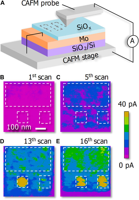
FIGURE 1. Contrasting background and filament conductivity dynamics at 7.7 V in our SiOx. (A) Schematic of CAFM instrumentation. (B–E) Evolution of the current in the 500 × 500 nm scanned area. The whole area becomes more conductive with successive scans, and two filaments appear. Note the color bar saturates at 40 pA, though the current in the filaments reaches saturation, at 12.3 nA. The dashed white boxes indicate the background and filament regions sampled for Figure 2.
RRAM behavior is predominantly attributed to filament dynamics (Ielmini, 2016), in some cases in parallel with a static background resistance or capacitance (Mehonic et al., 2012a), as we have also previously observed in SiOx (Mehonic et al., 2013). However, our observations in Figure 1 demonstrate that the background may also be dynamic, as the whole scan area was modified by electrical stress. NbOx RRAM devices have been reported to conduct via a core (filament) in parallel with a shell (background) (Li et al., 2019; Nandi et al., 2019). The combination of two parallel channels can give rise to complex oscillatory dynamics—important for neuromorphic applications. We suggest that such a core/shell model might be valid for many RRAM materials. An important consideration that emerges from this previous work is that dynamic device performance and functionality might require both a core and a shell, although in smaller devices, close to the size of an individual filament, the background component may disappear. We add the caveat that, here, the CAFM probe is a mobile electrode and does not address the whole scan area simultaneously.
Figure 2A shows the evolution of the background current compared to that through each of the filaments shown in Figures 1B–E. Up to scan 8, each region demonstrates a similar increase in mean current (i.e. the average of the pixels enclosed by the dashed boxes in Figures 1B–E). This is schematically illustrated in Figure 2B, wherein the electric field produces defects across the whole scan area, increasing the conductivity of the active layer. This is consistent with our previous report that electrically biasing silicon oxide results in large scale changes in the distribution of oxygen (Mehonic et al., 2016). After scan 9, the maximum current in the left-hand filament increases rapidly, saturating the detector in scan 11. Notably, the mean current lags the maximum by 2–3 scans. The high maximum current suggests the full formation of a filament through the SiOx, as shown in Figure 2C. The slower increase in mean current suggests lateral filament growth, as the region showing high current expands (as illustrated in Figure 2D and shown experimentally in Supplementary Figure S1). We can describe these processes as a gradual potentiation of a connection between the CAFM probe and the molybdenum bottom electrode. Scans 12 and 13 demonstrate stable current, corresponding to a stable filament. However, from scan 14 onwards, the mean current decreases, though the maximum remains at saturation. This suggests that the filament may be narrowing, as shown in Figure 2E, corresponding to depression of the connection between the probe and bottom electrode, a regime in which Joule heating induces sufficient defect neutralization, through re-oxidation, disrupting the filament but not fully breaking it. We also note the onset of potentiation at scan 12 for the right-hand filament. We expect that the difference in the behavior between the two filaments (i.e. the number of scans required to potentiate the sample at each locations) results from the intrinsic stochasticity of filament formation, arising from the amorphous nature of the SiOx (local roughness and density variations).
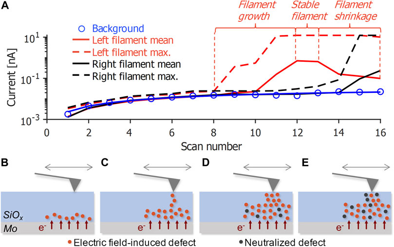
FIGURE 2. (A) Comparison of currents through the background matrix, and left- and right-hand filaments at a constant bias of 7.7 V, corresponding to the regions denoted by the dashed boxes in Figures 1B–E (B–E) Schematic representations of the growth and rupture of the left-hand filament, as defects are induced by the electric field and neutralized by Joule heating.
Following the disruption of the left-hand filament in Figure 1 and Figure 2, we scanned a larger area at a reduced stress of 5.5 V to try to pause the evolution of the right-hand filament. This voltage was chosen as it was sufficient to produce contrast in the current imaging between the surrounding, pristine sample area and the stressed region, without inducing any further changes (Supplementary Figure S4 demonstrates that voltages between 1V and 5 V did not produce any measurable current). Figure 3A demonstrates the current map after a single reading scan at a reduced stress of 5.5 V. Both filaments are still intact, although their positions are slightly different to Figure 1E. It is possible that we are only observing the most conductive part of each filament because the reading voltage, and thus the current, is much lower. The position and shape of the left-hand filament, in particular, is quite different. This might be a charging artefact or the result of surface contamination, or perhaps the appearance of a new filament, although this is unlikely as the reduced voltage was insufficient to produce any other change in conductivity. Topographical images show that the entire scan area, including that scanned only at 5.5 V, appears smoother than the pristine SiOx (Supplementary Figure S4 and Supplementary Figure S5). We expect this to result from deformation of the SiOx and/or molybdenum, rather than probe blunting, as we have previously discussed (i.e. that the imaging quality of this probe was maintained, as shown in Supplementary Figure S3). Interestingly, this may suggest that some structural change occurs at voltages below 7.7 V, below that required to observe pronounced changes in electrical behavior. Alternatively, those changes occurring at 7.7 V may have a de-localized distribution within the active layer or bottom electrode, affecting an area larger than the addressed region.
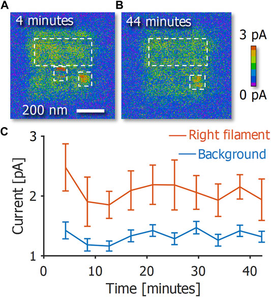
FIGURE 3. Persistence of the filament and background conductivity. (A) Current map of the area stressed in Figure 1, following a single reading scan at 5.5 V. The central area (green) is more conductive than the surroundings (blue), with higher currents at the location of each filament (red), the locations of which are indicated by the smaller white boxes. (B) Current map 40 min after a. The current in both the stressed region and the right-hand filament are unchanged, but the left-hand filament has disappeared. (C) The mean current in the stressed region and the right-hand filament, as indicated by the dashed white boxes in (A,B), over 40 min of reading. There is no significant change to either the filament or the stressed region.
The previously stressed area in Figure 3A is more conductive that its surroundings. Figure 3B shows the area following an additional 40 min of reading scans (10 consecutive scans in total). The background current and right-hand filament appear consistent with Figure 3A, but the left-hand filament has disappeared; this occurred after 2 scans. Figure 3C shows the mean current in the stressed region and the right-hand filament over the course of the reading measurements, neither of which changes significantly. Thus, we have been able to potentiate and depress a filament through the use of CAFM pseudopulses, and to stabilize a potentiated filament by reducing the applied voltage.
The consistency of the current in the stressed area during the reading measurements suggests that capacitive charging has not occurred, as we would expect the current to decrease over time if this was the case. Furthermore, such areas do not exhibit evidence of discharging when the CAFM probe is held in a fixed position, applying a constant voltage stress in either polarity. Therefore, the increase in conductivity appears to be a real, persistent effect. This further supports a core/shell model with a significant parallel background component.
Neuromorphic Filamentary Dynamics
To more directly study the temporal dynamics of filaments in our SiOx, we used CAFM to apply constant voltage stresses at fixed locations. Figure 4A demonstrates the typical time dependence of the current under a constant stress of 4 V. Initially, there is no measurable deviation in current from the noise floor (period i). The current then begins measurably increasing, initially quite slowly (period ii), then more rapidly (period iii); as a filament begins to form, the effective dielectric thickness will decrease and so the electric field will increase, causing positive feedback in the filament formation. Finally, the current jumps beyond 1 nA, then fluctuates across nearly two orders of magnitude and eventually saturates the detector (period iv). In this final period, we observe the competition between filament formation and rupture. We note that over the long duration of this measurement, some lateral drift occurred, which might lead to an overestimate of the time taken for the current to change (as shown in Supplementary Figure S6). It is also interesting that the topography of the local area appears consistent before and after the application of the voltage stress, although the addressed location shows a slight deformation. This leads us to conclude that the probe was not significantly affected by the measurement (i.e. no significant blunting or platinum deposition occurred, as imaging quality is maintained), although the SiOx or molybdenum might have deformed slightly.
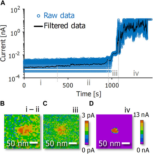
FIGURE 4. Time dependence of the current under constant voltage stress in SiOx. (A) With 4 V applied, the current increase accelerates over periods i to iii, eventually reaching instability and detector saturation in period iv. The raw data points are very dense, so data processed with a 1 s wide Savitzky-Golay filter are shown for clarity. (B–E) Evolution of the filament location during each period, taken from a different measurement to that shown in (A).
We imaged the top of a filament periodically during voltage stressing to assess its appearance following the application of increasing current, corresponding to the periods shown in Figure 4A (i.e. a different filament to that shown in Figure 4A). We initially applied 4.5 V to produce a few pA (equivalent to period i—ii), then 6 V to produce around 10 pA (equivalent to period iii), and 6 V again to produce current fluctuations between 100 pA and 10 nA (equivalent to period iv). Figures 4B–D shows current maps at equivalent periods to those shown in Figure 4A. Following periods i and ii, we observe a spot of a few pA above background when scanning at 7.8 V. We note that this voltage might affect the conductivity of the SiOx, although we were unable to resolve the spot at lower bias. However, from the trend in Figure 2A, we would not expect the effect of imaging at 7.8 V to be significant compared to the effect at the contact location when the probe is held in place for a longer duration at lower bias. The appearance of the spot does not change significantly following period iii; the conductivity increase appears not to persist once the voltage is removed. Finally, in period iv, the spot becomes much more pronounced and we measure a current at the saturation level of 12.3 nA. This highly conductive spot persisted at the measured location, such that we were able to perform current-voltage sweeps to ±50 mV, giving us Ohmic behavior below saturation, and a resistance of around 2.3 kΩ, although we note that the contact resistance between the probe and sample is unknown. Thus, although the current is unstable in period iv, this region corresponds to the presence of a filament across the SiOx. In fact, it is this rich, dynamic interplay between filament formation and rupture that gives rise to valuable neuromorphic functionalities such as spiking (Mehonic and Kenyon, 2016). Corresponding topography images for this measurement demonstrate the appearance of a transient distortion on the sample surface (Supplementary Figure S6). We expect this to be either a charging artefact or a deformation of the SiOx and/or molybdenum that subsequently relaxes. Otherwise, the local area retains its appearance, so we do not expect significant probe blunting to have occurred.
We have previously observed neuromorphic spiking in larger devices (Mehonic et al., 2012a). In both biology and electronic systems, this behavior describes the capacity of neurons to generate an output spike (action potential) once a threshold input has been reached (Merolla et al., 2011). Although we will not discuss the details of behavioral models here, the key functional importance of spiking is that it provides extremely low-power communication between neurons, (Milo et al., 2020), wherein the synaptic weight (the strength of the connection) determines the likelihood of an output being generated in response to a given input (Mehonic et al., 2019). To explore the neuromorphic dynamics of SiOx at the nanoscale, we applied constant-current stresses at fixed locations using CAFM, to create filaments and push them into voltage instability without saturating the current detector and risking hard breakdown. The target current was set, then the voltage limit was increased at around 1 V s−1, with the applied voltage sampled at 200 Hz. Currents ranging from 10 pA to 10 nA were sampled at an instrumental sensitivity of 1 nAV−1, and those ranging from 25 to 100 nA were sampled at a sensitivity of 100 nA−1. As shown in Figure 5A, once the voltage limit is high enough, the current jumps above its target as a filament is formed. The applied voltage is then reduced to reduce the current to its setpoint. However, as is clear in Figure 5A, the voltage required to maintain the current setpoint is not stable, and we observe many spikes of varying magnitude.
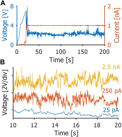
FIGURE 5. Spiking dynamics under constant current bias. No data processing filter has been applied. (A) The voltage response at a setpoint of 1 nA. Once the target current has been reached, the voltage spikes consistently for hundreds of seconds.(B) Spiking behavior at different current biases over 10 s. As the current setpoint is increased, we observe higher magnitude, more frequent spikes. The difference between 25 and 250 pA is clear, although between 250 pA and 2.5 nA it is less distinct.
Figure 5B shows the spiking dynamics taken from 10 s windows at three constant current biases. At 25 pA, the trace does not show many, if any, spikes. Rather, the voltage feedback is effectively “resting” and maintaining the current setpoint without any significant changes to the filament. However, increasing the setpoint to 250 pA produces clear, frequent spikes. This is reasonable, as a higher current will increase the likelihood of disrupting the filament via Joule heating. Each time the filament begins to break, its conductivity will decrease, and so the voltage must increase in order to reform the filament and maintain the setpoint. Thus, a spike will occur. Higher currents will produce greater Joule heating, and so we would expect the filament to be broken more quickly, increasing the frequency of spikes. However, it is not clear from Figure 5B how this behavior changes when the setpoint is increased from 250 pA to 2.5 nA.
To more quantitatively study the spiking dynamics in our SiOx, in Figure 6A we plot the mean spikes per second, SpS, defined as the total spikes counted in a measurement divided by the duration of counting in seconds, at a range of spike prominences, Vp. This corresponds to our detection threshold, i.e. we are determining whether or not to classify a given change in voltage as a spike (note that our CAFM produces a baseline noise of 0.4 mV when reading the sample bias at a fixed current setpoint, so our peak classification is statistically robust). Functionally, this represents the sensitivity of a connected component, such as another RRAM device, to input spikes. For all Vp, at low current bias, SpS is low, indicating that the voltage is in its resting state, with a reset unlikely to occur. As the current bias is increased, SpS also increases, as the filament is broken more frequently. This is a demonstration of a thresholding effect, wherein a low input current does not produce any output activation. Above 250 pA, a plateau is reached, with no further change as the current setpoint is increased by almost a further three orders of magnitude. We note that this plateaus in SpS is at around 35 per second, which is in good agreement with spike rates of 1–100 Hz reported in the literature, as well as our previous observations (Mehonic and Kenyon, 2016; Tang et al., 2019). As we increase Vp, SpS is lower at all values of Iset, though the shape of the trend remains consistent. This simply demonstrates that we record spikes more frequently if we have a lower detection threshold, as would be expected.
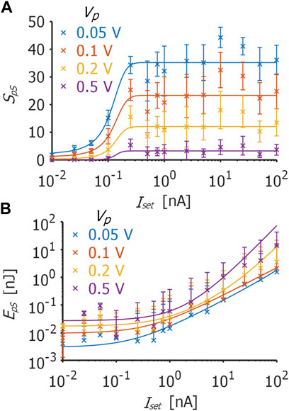
FIGURE 6. Characterization of neuromorphic behavior in our SiOx for a range of prominences, Vp. (A) Mean spikes per second, SpS, as a function of current bias, Iset. At lower detection thresholds, Vp, we detect more frequent spikes. Solid lines are hyperbolic tangent fits to the data; the R2 values are 0.97 (Vp = 0.05 V), 0.95 (Vp = 0.1 V), 0.79 (Vp = 0.2 V) and 0.69 (Vp = 0.5 V). Above 250 pA, SpS plateaus for all Vp. (B) Energy per spike, EpS, as a function of current bias, Iset. Solid lines are quadratic fits to the data; each has an R2 value of more than 0.99. Below 1 nA, EpS is in the range of a few tens of pJ for Vp up to 0.2 V. The error bars in each plot show the standard deviation, calculated by breaking the spiking signal into 50 sections and determining SpS and EpS for each section, to produce a distribution for the total signal. Note that the lower sections of many of the EpS error bars are not shown as they enter negative values.
The data in Figure 6A are, in all cases, fitted well by a hyperbolic tangent, according to:
where Smax is the maximum value of SpS for each Vp, I0 is the threshold current to transition to a spiking state (i.e. SpS > ½ Smax), and p characterizes the sharpness of this transition. We have previously used a hyperbolic tangent to model the reset coefficient in our devices, and would therefore expect a similar shape for SpS (Mehonic and Kenyon, 2016). However, we note that a logistic sigmoid was also a good fit for the data in Figure 6A. Both of these functions are continuous and non-linear, and are commonly implemented in transformations between layers in convolutional neural networks (Roy et al., 2019). Thus, functionally, SiOx appears able to produce a weighted output in response to inputs of varying magnitude. The additional decrease in the R2 value of the fitting as Vp increases demonstrates that more robust behavior, i.e. a more reliable output, would occur for a lower spike detection threshold. Phenomenologically, such logistic functions resemble the on/off activation and deactivation coefficients of the axonal ion pumps during generation of an action potential in a biological neuron (Gerstner et al., 2014; Tang et al., 2019). While a full functional and phenomenological classification of the spiking behavior of our devices with CAFM is beyond the scope of this work, it is very promising that we are able to observe these dynamics at the scale of individual filaments (Akinaga and Shima, 2010; Li et al., 2017; Tang et al., 2017), and at three orders of magnitude lower current than we have previously observed (Mehonic and Kenyon, 2016). Crucially, these observations confirm that neuromorphic functionality in RRAM devices can be a highly localized phenomenon, and is further encouragement that this behavior should persist as devices are scaled down.
It should be mentioned that we observed some topographical changes to the sample at the location of the probe contact point as a result of constant current stress measurements (Supplementary Figure S7). Up to 10 nA, these are a few nm in height, appearing similar to those observed following other measurements (Supplementary Figure S6), though they are not present following every applied stress. The appearance of the surrounding SiOx also does not change significantly after the stress has been applied, and we found no evidence of platinum on or in the SiOx following the application of up to 250 pA (Supplementary Figure S8). As such, we do not expect significant probe blunting or platinum deposition to have occurred at lower currents, suspecting instead that the SiOx and/or molybdenum have deformed. Conversely, above 10 nA the surface distortions are taller and the appearance of the surrounding material changes significantly, with the surface features appearing much wider and smoother. Therefore, we are unable to rule out probe blunting as a result of platinum deposition at higher currents. However, it is important to note that these values of Iset are well above the plateau in SpS, which occurs at around 250 pA, i.e. they are outside of the optimal range of device operation, so do not correspond to useful behavior in the present context. This suggests that platinum deposition is not responsible for the functionality discussed above, specifically a weighted output in response to the input current, following a logistic shape.
Information in a spiking neural network is encoded by the timing and frequency of spikes (Tang et al., 2019). As an event-based rather than continuous-output paradigm, this offers a very energy-efficient means of processing information, with both CMOS and RRAM devices demonstrating spikes of just a few fJ (Merolla et al., 2011; Wang et al., 2014; Sourikopoulos et al., 2017; Tang et al., 2019). We have estimated the energy per spike, EpS, in our CAFM measurements according to:
where WS and VS are the full width at half maximum (which is log-normally distributed, so we have used the modal value) and height (which is normally distributed, so we have used the mean value) of spikes, respectively, at a current bias of Iset. As shown in Figure 6B, for all Vp, EpS increases quadratically with Iset; this seems reasonable, given that the spiking voltage should be a function of the current, according to Ohm’s law. Up to around 1 nA current bias, we can see that EpS is up to a few tens of pJ, except for Vp of 0.5 V, which is around 100 pJ as we are excluding the peaks of lower prominence and thus lower height. Therefore, for a device operating up to the SpS plateau observed in Figure 6A, we can expect the spike energy to be a few tens of pJ; increasing the current would not produce more spikes, though it would increase EpS.
We expect that EpS would be reduced through optimization of the experimental setup. Using a CAFM probe as an electrode necessitates higher operational voltages, due to the high contact resistance that would not be present with a deposited top electrode (Mehonic et al., 2015). and we have previously observed that less than 1 V may be used to switch devices with a top gold electrode and a 37 nm SiOx switching layer (Mehonic et al., 2017b), more than three times the thickness of the layer used in the present work. Furthermore, the voltage feedback of our microscope is slower than might be achieved with a semiconductor parameter analyzer, with which we have observed switching processes to take place in tens of nanoseconds (Montesi et al., 2016). Therefore, we cautiously estimate, for a 100 nanosecond-wide spike at 1 V and 250 pA, an EpS of 25 aJ. This is a highly efficient event, representing the communication of information between devices, or changing in weight of a particular connection, with an energy consumption two orders of magnitude lower than that of conventional CMOS or other RRAM devices (Merolla et al., 2011; Wang et al., 2014; Sourikopoulos et al., 2017; Tang et al., 2019). We are able to propose such a low value because the threshold for our SiOx to enter into a spiking state can be a very low current. If we consider an ideal, lossless, 1 cm × 1 cm RRAM array composed of 100 × 100 nm devices (i.e. around 25 × 108 devices), each firing at a rate of 10 Hz, an EpS of 25 aJ leads to a hypothetical power consumption of 0.6 µWcm−2, more than four orders of magnitude lower than that of the human brain, which consumes around 10 mWcm−2 (Young et al., 2019). While this is hypothetical, as any real system will have a reduced efficiency due to line losses and device variability, for example, this is nevertheless a very exciting prospect for low power, high density neuromorphic computation.
Finally, we note that the behavior presented in this work is also observed at other locations and on other samples, although a full statistical quantification of these effects across samples of, for example, differing active layer thickness, or bottom electrode material, is beyond the scope of this manuscript.
Conclusion
In this work, we have demonstrated the use of CAFM as a tool for studying the plasticity and neuromorphic dynamics of SiOx at the nanoscale. The behavior that we observe is in line with that of larger devices, although at a significantly lower energy of 25 aJ, which is very encouraging from the perspective of scaling and power consumption to produce significantly more efficient neuromorphic devices than those of conventional CMOS or other RRAM materials. More specifically, this equates to a power consumption of less than 1 µWcm−2, which is lower than that of the human brain. While we would expect losses and inefficiencies to be present in fully-integrated hardware, the prospect of such low device power requirements suggests the potential for great reductions in energy consumption for complex computations, such as are currently required in machine learning. Thus, there is great potential for reducing the carbon footprint of emerging techniques that require huge energy inputs for handling very large quantities of data.
We have additionally shown that not only do filamentary locations demonstrate conductivity enhancement, but that the surrounding background material also becomes more conductive under electrical stress. This core/shell behavior is an important finding, supporting the conclusions of previous work and suggesting that this parallel nature of RRAM devices could be the source of rich dynamic behavior that may be exploited in novel neuromorphic systems.
We have established that the instabilities in the behavior of individual filaments are well-suited to neuromorphic functionality. The interplay of filament formation and rupture produces gradual plasticity under repeated electrical stressing, as well as voltage spiking under constant current stress. In the case of spiking, SiOx exhibits a current dependence that is fitted well by a continuous, logistic-type function, which suggests promising behavior for neuromorphic computation. However, a full classification of the nanoscale neuromorphic behavior of our SiOx is certainly necessary future work to fully understand these phenomena and further develop their functionalities. In particular, a thorough investigation of spike dynamics in nanoscale devices, including consideration of any background components is essential to fully understand their capacity for low-energy, high density neuromorphic applications.
Data Availability Statement
The raw data supporting the conclusion of this article will be made available by the authors, without undue reservation.
Author Contributions
MB: Designed the study, performed the CAFM measurements, analyzed data and prepared the manuscript; WN: Fabricated the devices and optimized their performance; DM: Assisted with interpretation of the data and preparation of the manuscript; HC: Performed secondary ion mass spectroscopy measurements, and analyzed and interpreted associated data; SH: Assisted with CAFM instrumentation and study design; AM: Assisted with study design and device optimization; AK: Oversaw the work and assisted with study refinement and interpretation of the data.
Funding
This work was supported by the Engineering and Physical Sciences Research Council, United Kingdom (grant no. EP/K01739X/1) Leverhulme Trust (grant no. RPG-2016-135) and The Worshipful Company of Scientific Instrument Makers.
Conflict of Interest
The authors declare that the research was conducted in the absence of any commercial or financial relationships that could be construed as a potential conflict of interest.
The handling Editor declared a past co-authorship with the authors (AK, DM).
Publisher’s Note
All claims expressed in this article are solely those of the authors and do not necessarily represent those of their affiliated organizations, or those of the publisher, the editors and the reviewers. Any product that may be evaluated in this article, or claim that may be made by its manufacturer, is not guaranteed or endorsed by the publisher.
Supplementary Material
The Supplementary Material for this article can be found online at: https://www.frontiersin.org/articles/10.3389/fnano.2021.699037/full#supplementary-material
References
Akinaga, H., and Shima, H. (2010). Resistive Random Access Memory (ReRAM) Based on Metal Oxides. Proc. IEEE 98, 2237–2251. doi:10.1109/jproc.2010.2070830
Baeumer, C., Schmitz, C., Ramadan, A. H. H., Du, H., Skaja, K., Feyer, V., et al. (2015). Spectromicroscopic Insights for Rational Design of Redox-Based Memristive Devices. Nat. Commun. 6, 8610. doi:10.1038/ncomms9610
Blasco, X., Hill, D., Porti, M., Nafría, M., and Aymerich, X. (2001). Topographic Characterization of AFM-Grown SiO2on Si. Nanotechnology 12, 110–112. doi:10.1088/0957-4484/12/2/307
Bousoulas, P., Giannopoulos, J., Giannakopoulos, K., Dimitrakis, P., and Tsoukalas, D. (2015). Memory Programming of TiO2−x Films by Conductive Atomic Force Microscopy Evidencing Filamentary Resistive Switching. Appl. Surf. Sci. 332, 55–61. doi:10.1016/j.apsusc.2015.01.133
Bousoulas, P., Karageorgiou, I., Aslanidis, V., Giannakopoulos, K., and Tsoukalas, D. (2018). Tuning Resistive, Capacitive, and Synaptic Properties of Forming Free TiO2-X -Based RRAM Devices by Embedded Pt and Ta Nanocrystals. Phys. Status Solidi A. 215, 1700440. doi:10.1002/pssa.201700440
Buckwell, M., Montesi, L., Hudziak, S., Mehonic, A., and Kenyon, A. J. (2015). Conductance Tomography of Conductive Filaments in Intrinsic Silicon-Rich Silica RRAM. Nanoscale 7, 18030–18035. doi:10.1039/c5nr04982b
Buckwell, M., Ng, W. H., Hudziak, S., Mehonic, A., Lanza, M., and Kenyon, A. J. (2019). Improving the Consistency of Nanoscale Etching for Atomic Force Microscopy Tomography Applications. Front. Mater. 6, 1–17. doi:10.3389/fmats.2019.00203
Chen, S., Jiang, L., Buckwell, M., Jing, X., Ji, Y., Grustan-Gutierrez, E., et al. (2018). On the Limits of Scalpel AFM for the 3D Electrical Characterization of Nanomaterials. Adv. Funct. Mater. 28, 1802266. doi:10.1002/adfm.201802266
Clarke, H., Deremo, L., Anderson, J., Ganguli, S., and Shamberger, P. J. (2019). Conductive Filament Shape in HfO2 Electrochemical Metallization Cells under a Range of Forming Voltages. Nanotechnology 31, 075706. doi:10.1088/1361-6528/ab53a9
Cox, H. R. J., Buckwell, M., Ng, W. H., Mannion, D. J., Mehonic, A., Shearing, P. R., et al. (2021). A Nanoscale Analysis Method to Reveal Oxygen Exchange between Environment, Oxide, and Electrodes in ReRAM Devices. APL Mater. 9, 111109–9. doi:10.1063/5.0070046
Garcia, R., Martinez, R. V., and Martinez, J. (2006). Nano-chemistry and Scanning Probe Nanolithographies. Chem. Soc. Rev. 35, 29–38. doi:10.1039/b501599p
Gerstner, W., Kistler, W. M., Naud, R., and Paninski, L. (2014). “Hodgkin-Huxley Model,” in Neuronal Dynamics (Cambridge University Press). Available at: https://neuronaldynamics.epfl.ch/book.html.
Ielmini, D., Nardi, F., and Cagli, C. (2011). Universal Reset Characteristics of Unipolar and Bipolar Metal-Oxide RRAM. IEEE Trans. Electron. Devices 58, 3246–3253. doi:10.1109/TED.2011.2161088
Ielmini, D. (2016). Resistive Switching Memories Based on Metal Oxides: Mechanisms, Reliability and Scaling. Semicond. Sci. Technol. 31, 063002. doi:10.1088/0268-1242/31/6/063002
Ielmini, D. (2018). Brain-inspired Computing with Resistive Switching Memory (RRAM): Devices, Synapses and Neural Networks. Microelectron. Eng. 190, 44–53. doi:10.1016/j.mee.2018.01.009
Indiveri, G., Linares-Barranco, B., Legenstein, R., Deligeorgis, G., and Prodromakis, T. (2013). Integration of Nanoscale Memristor Synapses in Neuromorphic Computing Architectures. Nanotechnology 24, 384010. doi:10.1088/0957-4484/24/38/384010
Jaafar, A. H., Gray, R. J., Verrelli, E., O'Neill, M., Kelly, S. M., and Kemp, N. T. (2017). Reversible Optical Switching Memristors with Tunable STDP Synaptic Plasticity: A Route to Hierarchical Control in Artificial Intelligent Systems. Nanoscale 9, 17091–17098. doi:10.1039/c7nr06138b
Kenyon, A. J., Singh Munde, M., Ng, W. H., Buckwell, M., Joksas, D., and Mehonic, A. (2019). The Interplay between Structure and Function in Redox-Based Resistance Switching. Faraday Discuss. 213, 151–163. doi:10.1039/c8fd00118a
Kim, K. M., Jeong, D. S., and Hwang, C. S. (2011). Nanofilamentary Resistive Switching in Binary Oxide System; a Review on the Present Status and Outlook. Nanotechnology 22, 254002. doi:10.1088/0957-4484/22/25/254002
Lanza, M., Porti, M., Nafria, M., Benstetter, G., Frammelsberger, W., Ranzinger, H., et al. (2007). Influence of the Manufacturing Process on the Electrical Properties of Thin (<4 nm) Hafnium Based High-k Stacks Observed with CAFM. Microelectron. Reliab. 47, 1424–1428. doi:10.1016/j.microrel.2007.07.045
Lanza, M., Porti, M., Nafría, M., Aymerich, X., Benstetter, G., Lodermeier, E., et al. (2011). Conductivity and Charge Trapping after Electrical Stress in Amorphous and Polycrystalline $\hbox{Al}_{2}\Hbox{O}_{3}\hbox{-Based}$ Devices Studied with AFM-Related Techniques. IEEE Trans. Nanotechnol. 10, 344–351. doi:10.1109/TNANO.2010.2041935
Lanza, M., Wong, H.-S. P., Pop, E., Ielmini, D., Strukov, D., Regan, B. C., et al. (2019). Recommended Methods to Study Resistive Switching Devices. Adv. Electron. Mater. 5, 1800143. doi:10.1002/aelm.201800143
Lanza, M. (2014). A Review on Resistive Switching in High-K Dielectrics: A Nanoscale point of View Using Conductive Atomic Force Microscope. Materials 7, 2155–2182. doi:10.3390/ma7032155
Li, C., Han, L., Jiang, H., Jang, M.-H., Lin, P., Wu, Q., et al. (2017). Three-dimensional Crossbar Arrays of Self-Rectifying Si/SiO2/Si Memristors. Nat. Commun. 8, 15666. doi:10.1038/ncomms15666
Li, C., Belkin, D., Li, Y., Yan, P., Hu, M., Ge, N., et al. (2018). Efficient and Self-Adaptive In-Situ Learning in Multilayer Memristor Neural Networks. Nat. Commun. 9, 7–14. doi:10.1038/s41467-018-04484-2
Li, S., Liu, X., Nandi, S. K., Nath, S. K., and Elliman, R. G. (2019). Origin of Current‐Controlled Negative Differential Resistance Modes and the Emergence of Composite Characteristics with High Complexity. Adv. Funct. Mater. 29, 1905060. doi:10.1002/adfm.201905060
Mannion, D. J., Mehonic, A., Ng, W. H., and Kenyon, A. J. (2020). Memristor-Based Edge Detection for Spike Encoded Pixels. Front. Neurosci. 13, 1386. doi:10.3389/fnins.2019.01386
Mehonic, A., and Kenyon, A. J. (2016). Emulating the Electrical Activity of the Neuron Using a Silicon Oxide RRAM Cell. Front. Neurosci. 10, 57. doi:10.3389/fnins.2016.00057
Mehonic, A., Cueff, S., Wojdak, M., Hudziak, S., Jambois, O., Labbé, C., et al. (2012a). Resistive Switching in Silicon Suboxide Films. J. Appl. Phys. 111, 074507. doi:10.1063/1.3701581
Mehonic, A., Cueff, S., Wojdak, M., Hudziak, S., Labbé, C., Rizk, R., et al. (2012b). Electrically Tailored Resistance Switching in Silicon Oxide. Nanotechnology 23, 455201. doi:10.1088/0957-4484/23/45/455201
Mehonic, A., Vrajitoarea, A., Cueff, S., Hudziak, S., Howe, H., Labbé, C., et al. (2013). Quantum Conductance in Silicon Oxide Resistive Memory Devices. Sci. Rep. 3, 2708. doi:10.1038/srep02708
Mehonic, A., Buckwell, M., Montesi, L., Garnett, L., Hudziak, S., Fearn, S., et al. (2015). Structural Changes and Conductance Thresholds in Metal-free Intrinsic SiOx Resistive Random Access Memory. J. Appl. Phys. 117, 124505. doi:10.1063/1.4916259
Mehonic, A., Buckwell, M., Montesi, L., Munde, M. S., Gao, D., Hudziak, S., et al. (2016). Silica: Nanoscale Transformations in Metastable, Amorphous, Silicon-Rich Silica (Adv. Mater. 34/2016). Adv. Mater. 28, 7549. doi:10.1002/adma.201670241
Mehonic, A., Gerard, T., and Kenyon, A. J. (2017a). Light-activated Resistance Switching in SiOx RRAM Devices. Appl. Phys. Lett. 111, 233502. doi:10.1063/1.5009069
Mehonic, A., Munde, M. S., Ng, W. H., Buckwell, M., Montesi, L., Bosman, M., et al. (2017b). Intrinsic Resistance Switching in Amorphous Silicon Oxide for High Performance SiOx ReRAM Devices. Microelectron. Eng. 178, 98–103. doi:10.1016/j.mee.2017.04.033
Mehonic, A., Shluger, A. L., Gao, D., Valov, I., Miranda, E., Ielmini, D., et al. (2018). Silicon Oxide (SiO X ): A Promising Material for Resistance Switching? Adv. Mater. 30, 1801187. doi:10.1002/adma.201801187
Mehonic, A., Joksas, D., Ng, W. H., Buckwell, M., and Kenyon, A. J. (2019). Simulation of Inference Accuracy Using Realistic RRAM Devices. Front. Neurosci. 13, 593. doi:10.3389/fnins.2019.00593
Merolla, P., Arthur, J., Akopyan, F., Imam, N., Manohar, R., and Modha, D. S. (2011). “A Digital Neurosynaptic Core Using Embedded Crossbar Memory with 45pJ Per Spike in 45nm,” in 2011 Custom Integrated Circuits Conference, San Jose, CA, September 19–21, 2011. (IEEE), 1–4. doi:10.1109/CICC.2011.6055294
Milo, V., Malavena, G., Monzio Compagnoni, C., and Ielmini, D. (2020). Memristive and CMOS Devices for Neuromorphic Computing. Materials 13, 166. doi:10.3390/ma13010166
Montesi, L., Buckwell, M., Zarudnyi, K., Garnett, L., Hudziak, S., Mehonic, A., et al. (2016). Nanosecond Analog Programming of Substoichiometric Silicon Oxide Resistive RAM. IEEE Trans. Nanotechnol. 15, 428–434. doi:10.1109/TNANO.2016.2539925
Moon, K., Lim, S., Park, J., Sung, C., Oh, S., Woo, J., et al. (2019). RRAM-based Synapse Devices for Neuromorphic Systems. Faraday Discuss. 213, 421–451. doi:10.1039/c8fd00127h
Munde, M. S., Mehonic, A., Ng, W. H., Buckwell, M., Montesi, L., Bosman, M., et al. (2017). Intrinsic Resistance Switching in Amorphous Silicon Suboxides: The Role of Columnar Microstructure. Sci. Rep. 7, 9274. doi:10.1038/s41598-017-09565-8
Nandi, S. K., Nath, S. K., El‐Helou, A. E., Li, S., Liu, X., Raad, P. E., et al. (2019). Current Localization and Redistribution as the Basis of Discontinuous Current Controlled Negative Differential Resistance in NbO X. Adv. Funct. Mater. 29, 1906731–1906738. doi:10.1002/adfm.201906731
Polspoel, W., and Vandervorst, W. (2007). Evaluation of Trap Creation and Charging in Thin SiO2 Using Both SCM and C-AFM. Microelectronic Eng. 84, 495–500. doi:10.1016/j.mee.2006.10.074
Porti, M., Nafría, M., and Aymerich, X. (2004). Nanometer-Scale Analysis of CurrentLimited Stresses Impact on SiO$_2$Gate Oxide Reliability Using C-AFM. IEEE Trans. Nanotechnol. 3, 55–60. doi:10.1109/TNANO.2004.824023
Roy, K., Jaiswal, A., and Panda, P. (2019). Towards Spike-Based Machine Intelligence with Neuromorphic Computing. Nature 575, 607–617. doi:10.1038/s41586-019-1677-2
Sourikopoulos, I., Hedayat, S., Loyez, C., Danneville, F., Hoel, V., Mercier, E., et al. (2017). A 4-fJ/spike Artificial Neuron in 65 Nm CMOS Technology. Front. Neurosci. 11, 123. doi:10.3389/fnins.2017.00123
Šuch, O., Klimo, M., Kemp, N. T., and Škvarek, O. (2018). Passive Memristor Synaptic Circuits with Multiple Timing Dependent Plasticity Mechanisms. AEU - Int. J. Electron. Commun. 96, 252–259. doi:10.1016/j.aeue.2018.09.025
Szot, K., Dittmann, R., Speier, W., and Waser, R. (2007). Nanoscale Resistive Switching in SrTiO3 Thin Films. Phys. Stat. Sol. (Rrl) 1, R86–R88. doi:10.1002/pssr.200701003
Tang, K., Meng, A. C., Hui, F., Shi, Y., Petach, T., Hitzman, C., et al. (2017). Distinguishing Oxygen Vacancy Electromigration and Conductive Filament Formation in TiO2 Resistance Switching Using Liquid Electrolyte Contacts. Nano Lett. 17, 4390–4399. doi:10.1021/acs.nanolett.7b01460
Tang, J., Yuan, F., Shen, X., Wang, Z., Rao, M., He, Y., et al. (2019). Bridging Biological and Artificial Neural Networks with Emerging Neuromorphic Devices: Fundamentals, Progress, and Challenges. Adv. Mater. 31, 1902761. doi:10.1002/adma.201902761
Thompson, N. C., Greenewald, K., Lee, K., and Manso, G. F. (2021). Deep Learning's Diminishing Returns: The Cost of Improvement Is Becoming Unsustainable. IEEE Spectr. 58, 50–55. doi:10.1109/MSPEC.2021.9563954
Wang, I.-T., Lin, Y.-C., Wang, Y.-F., Hsu, C.-W., and Hou, T.-H. (2014). “3D Synaptic Architecture with Ultralow Sub-10 fJ Energy Per Spike for Neuromorphic Computation,” in 2014 IEEE International Electron Devices Meeting, San Francisco, CA, USA, December 15–17, 2014. (IEEE), 28.5.1–28.5.4. doi:10.1109/IEDM.2014.7047127
Waser, R. (2009). Resistive Non-volatile Memory Devices (Invited Paper). Microelectron. Eng. 86, 1925–1928. doi:10.1016/j.mee.2009.03.132
Wedig, A., Luebben, M., Cho, D.-Y., Moors, M., Skaja, K., Rana, V., et al. (2015). Nanoscale Cation Motion in TaOx, HfOx and TiOx Memristive Systems. Nat. Nanotech 11, 67–74. doi:10.1038/nnano.2015.221
Yang, Y., Gao, P., Gaba, S., Chang, T., Pan, X., and Lu, W. (2012). Observation of Conducting Filament Growth in Nanoscale Resistive Memories. Nat. Commun. 3, 732. doi:10.1038/ncomms1737
Yoshida, C., Kinoshita, K., Yamasaki, T., and Sugiyama, Y. (2008). Direct Observation of Oxygen Movement during Resistance Switching in NiO/Pt Film. Appl. Phys. Lett. 93, 042106. doi:10.1063/1.2966141
Young, A. R., Dean, M. E., Plank, J. S., and S. Rose, G. G. (2019). A Review of Spiking Neuromorphic Hardware Communication Systems. IEEE Access 7, 135606–135620. doi:10.1109/access.2019.2941772
Zarudnyi, K., Mehonic, A., Montesi, L., Buckwell, M., Hudziak, S., and Kenyon, A. J. (2018). Spike-timing Dependent Plasticity in Unipolar Silicon Oxide RRAM Devices. Front. Neurosci. 12, 1–8. doi:10.3389/fnins.2018.00057
Zhang, Y., Zhou, Z., Huang, P., Fan, M., Han, R., Shen, W., et al. (2019). “An Improved Hardware Accelaration Architecture of Binary Neural Network with 1T1R Array Based Forward/backward Propagation Module,” in 2019 Silicon Nanoelectronics Workshop (SNW), Kyoto, Japan, June 9–10, 2019, 1–2. doi:10.23919/SNW.2019.8782967
Keywords: conductive atomic force microscopy, filament, plasticity, spiking, neuromorphic, RRAM, memristor, silicon
Citation: Buckwell M, Ng WH, Mannion DJ, Cox HRJ, Hudziak S, Mehonic A and Kenyon AJ (2021) Neuromorphic Dynamics at the Nanoscale in Silicon Suboxide RRAM. Front. Nanotechnol. 3:699037. doi: 10.3389/fnano.2021.699037
Received: 22 April 2021; Accepted: 07 December 2021;
Published: 22 December 2021.
Edited by:
Carlo Ricciardi, Politecnico di Torino, ItalyReviewed by:
Amirkianoosh Kiani, Ontario Tech University, CanadaGianluca Milano, National Institute of Metrological Research (INRiM), Italy
Copyright © 2021 Buckwell, Ng, Mannion, Cox, Hudziak, Mehonic and Kenyon. This is an open-access article distributed under the terms of the Creative Commons Attribution License (CC BY). The use, distribution or reproduction in other forums is permitted, provided the original author(s) and the copyright owner(s) are credited and that the original publication in this journal is cited, in accordance with accepted academic practice. No use, distribution or reproduction is permitted which does not comply with these terms.
*Correspondence: Mark Buckwell, markbuckwell@ucl.ac.uk