Fault Injection Attacks in Spiking Neural Networks and Countermeasures
 Karthikeyan Nagarajan
 Junde Li
 Sina Sayyah Ensan
 Sachhidh Kannan2
  Swaroop Ghosh
- 1School of Electrical Engineering and Computer Science, Penn State University, University Park, PA, United States
- 2Ampere Computing, Portland, OR, United States
Spiking Neural Networks (SNN) are fast emerging as an alternative option to Deep Neural Networks (DNN). They are computationally more powerful and provide higher energy-efficiency than DNNs. While exciting at first glance, SNNs contain security-sensitive assets (e.g., neuron threshold voltage) and vulnerabilities (e.g., sensitivity of classification accuracy to neuron threshold voltage change) that can be exploited by the adversaries. We explore global fault injection attacks using external power supply and laser-induced local power glitches on SNN designed using common analog neurons to corrupt critical training parameters such as spike amplitude and neuron’s membrane threshold potential. We also analyze the impact of power-based attacks on the SNN for digit classification task and observe a worst-case classification accuracy degradation of −85.65%. We explore the impact of various design parameters of SNN (e.g., learning rate, spike trace decay constant, and number of neurons) and identify design choices for robust implementation of SNN. We recover classification accuracy degradation by 30–47% for a subset of power-based attacks by modifying SNN training parameters such as learning rate, trace decay constant, and neurons per layer. We also propose hardware-level defenses, e.g., a robust current driver design that is immune to power-oriented attacks, improved circuit sizing of neuron components to reduce/recover the adversarial accuracy degradation at the cost of negligible area, and 25% power overhead. We also propose a dummy neuron-based detection of voltage fault injection at ∼1% power and area overhead each.
1 Introduction
Artificial Neural Networks (ANNs or NNs) that are inspired by the functionality of human brains consist of layers of neurons that are interconnected through synapses and can be used to approximate any computable function. The advent of neural networks in safety-critical domains such as autonomous driving (Kaiser et al., 2016), healthcare (Azghadi et al., 2020), Internet of Things (Whatmough et al., 2018), and security (Cao et al., 2015) warrants the need to investigate their security vulnerabilities and threats. An attack on a neural network can lead to undesirable or unsafe decisions in real-world applications (e.g., reduced accuracy or confidence in road sign identification during autonomous driving). These attacks can be initiated at either the production, training, or final application phases.
Spiking Neural Networks (SNNs) (Maass, 1997) are the third generation of neural networks. SNNs are emerging as an alternative to Deep Neural Networks (DNNs) since they are biologically plausible, computationally powerful (Heiberg et al., 2018), and energy-efficient (Merolla et al., 2014; Davies et al., 2018; Tavanaei et al., 2019). However, very limited research exists on the security of SNNs against adversarial attacks. Broadly, the attacks could be classified as (1) white box attacks where an attacker has complete knowledge of the SNN architecture, and (2) black box attacks where the attacker does not know the SNN architecture, network parameters, or training data.
Multiple prior works such as (Goodfellow et al., 2014; Kurakin et al., 2016), and (Madry et al., 2017) investigate adversarial attacks on DNN, e.g., non-detectable changes to input data causing a classifier to mispredict with a higher probability and suggest countermeasures. The vulnerabilities/attacks of SNNs under a white box scenario, e.g., sensitivity to adversarial examples and a robust training mechanism for defense is proposed (Bagheri et al., 2018). A white box fault injection attack is proposed (Venceslai et al., 2020) in SNNs through adversarial input noise. A black box attack to generate adversarial input examples for SNNs to cause misprediction is proposed in (Marchisio et al., 2020). However, these white and black box attacks on SNN do not study the effects of voltage/power-based fault injection attacks.
Prior works have shown that voltage fault injection (VFI) techniques can be used as an effective side channel attack to disrupt the execution flow of a system. In (Barenghi et al., 2012), a fault injection technique is proposed for cryptographic devices that underpowers the device to introduce bit errors. In (Bozzato et al., 2019), novel VFI techniques are proposed to inject glitches in popular microcontrollers from manufacturers such as STMicroelectronics and Texas Instruments. In (Zussa et al., 2013), negative power supply glitch attack has been introduced on FPGA to cause timing constraint violations. Local voltage and clock glitching attacks have also been proposed using laser exposure. However, such studies are not performed for SNN.
Proposed Threat Model
There is a limited amount of research on SNN attacks (except adversarial input-based attacks). Similar to classical systems, the adversary can manipulate the supply voltage or inject voltage glitches in the SNN systems. This is likely for (1) an external adversary who has physical possession of the device or the power port, (2) an insider adversary with access to a power port or laser gun to inject the fault. In this paper, we study seven attacks under black box and white box scenarios.
Black Box Attack
In this scenario (Attack 7 in Section 4.4), the adversary affects the power supply of the entire system to (1) corrupt spiking amplitude of SNN neuron input and (2) disrupt SNN neuron’s membrane functionality. The adversary does not need to know the SNN architecture but needs to control the external power supply (VDD) to launch this attack. Figure 1 shows a high-level schematic of the proposed threat model against an SNN, where an input image to be classified is converted to spike trains and fed to the neuron layers. The objective is to degrade accuracy of the classified digit. Note that the neuron layers, neurons, and their interconnections shown in Figure 1 just illustrate the proposed threat model. The SNN architecture actually implemented in this paper is explained in Section 4.1.
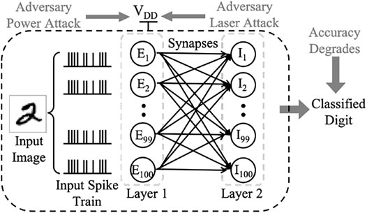
FIGURE 1. Threat model for power-based attacks on SNN.
White Box Attacks
In this scenario, we consider the following cases (details in Section 4.2) where the adversary is able to individually attack SNN layers and peripherals through localized laser-based power fault injection 1) Attack 1 where only peripherals, e.g., input current drivers are attacked, 2) Attack 2, 3, and 4 where individual SNN layers attacked partially to fully, i.e., 0–100%, 3) Attack 5 where all SNN layers affected (no peripherals), and 4) Attack 6 where the timing of the attacks on individual layers varies from 0 to 100% of training/inference phase.
Contributions: In summary, we.
•Present detailed analysis of two neuron models, namely, Axon Hillock neuron and voltage I&F amplifier neuron under global, local and fine-grain supply voltage variation
•Propose seven power-based attack models against SNN designs under black box and white box settings
•Analyze the impact of proposed attacks for digit classification tasks
•Analyze the sensitivity of various design parameters of SNN learning algorithm (STDP) to fault injection attack
•Propose hardware defenses and a novel detection technique
In the remainder of the paper, Section 2 presents background on SNNs and neuron design, Section 3 proposes the attack models, Sections 4 and 5 present the analysis of the attack and countermeasures, respectively, Section 6 presents some discussion and, finally, Section 7 draws the conclusion.
2 Background
In this section, we present the overview of SNN and neuron designs (Indiveri et al., 2011) that have been used in this paper.
2.1 Overview of Spiking Neural Network
SNNs consist of layers of spiking neurons that are connected to adjacent neurons using synaptic weights (Figure 1). The neurons between adjacent layers exchange information in the form of spike trains. The critical parameters for SNN operation include the timing of the spikes and the strengths of the synaptic weights between neurons. Each neuron includes a membrane, whose potential increases when the neuron received an input spike. When this membrane potential reaches a pre-designed threshold, the neuron fires an output spike. Various neuron models such as I&F, Hodgkin-Huxley, and spike response exist with different membrane and spike-generation operations. In this work, we have implemented two flavors of I&F neuron to showcase the power-based attacks.
2.2 Neuron Model
In this work, we have used Leaky Integrate and Fire (LIF) neuron models where the temporal dynamics are represented by:
Here, v(t) is the membrane potential, τmem is the membrane time constant, vrest is the resting potential and I(t) represents the summation of inputs from all synaptic inputs to the neuron. When the membrane voltage reaches a pre-designed vth(t), it fires an output spike and its membrane potential resets to vreset. The neuron’s membrane potential is fixed for a refractory period of δref. For neural network implementation, we have used the (Diehl et al., 2015) LIF neuron feature of adaptive thresholding scheme where each neuron follows these temporal dynamics:
Here, the constant θ0 > vrest, vreset and τtheta is the adaptive threshold time constant. When a neuron receives a spike, θ(t) is increased by a constant value of θ+ and then decays exponentially as shown in Eq. 2.
2.3 Synaptic Learning Model
Hebbian Learning: In Hebbian learning (Hebb, 2005), correlated activation of pre- and post-synaptic neurons leads to the strengthening of synaptic weights between two neurons. The basic Hebbian learning rule is expressed as:
Here Δw denotes the change in synaptic weight, x refers to the array of input spikes on the neuron’s synapses, η is the learning rate, and w is the synaptic weight associated with the neuron. Term y (x, w) denotes the post-synaptic activation of the neuron which is a function of the input and the weights.
Spike Time Dependent Plasticity
Hebbian learning is often implemented as STDP (a more quantitative form). STDP is adopted as a learning rule where the synaptic strengths between two neurons are determined by their relative timing of spiking. The change in synaptic weight (Δw) is represented by:
Here, ηpre and ηpost represent the pre- and post-synaptic learning rates, τt denotes the spike trace decay time constant, and Δt represents the relative spike timing difference between connected neurons. When Δt is close to 0, the exponential part of the equation is set very close to 1 and decays exponentially to 0 with spike trace decay time constant (τt).
2.4 Neuron Design and Implementation
In this work, all neuron models are implemented and analyzed on HSPICE using PTM 65 nm technology.
2.4.1 Axon Hillock Spiking Neuron Design
The Axon Hillock circuit (Mead and Ismail, 2012) (Figure 2A) consists of an amplifier block implemented using two inverters in series (shown in dotted gray box). The input current (Iin) is integrated at the neuron membrane capacitance (Cmem), and the analog membrane voltage (Vmem) rises linearly until it crosses the amplifier’s threshold. Once it reaches this point, the output (Vout) switches from “0” to VDD. This Vout is fed back into a reset transistor (MN1) and activates a positive feedback through the capacitor divider (Cfb). Another transistor (MN2), controlled by Vpw, determines the reset current. If reset current
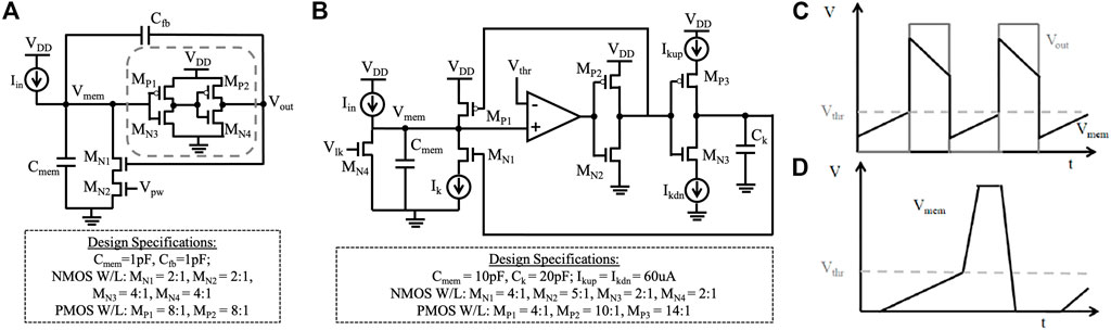
FIGURE 2. (A) Axon Hillock circuit; (B) voltage amplifier I&F circuit; (C) expected membrane voltage and output voltage of Axon Hillock neuron; (D) expected membrane voltage of I&F neuron.
In this paper, the value of the membrane capacitance (Cmem) and the feedback capacitance (Cfb) of 1pF are used. For experimental purposes, the input current spikes with an amplitude of 200 nA, a spike width of 25 ns, and a spike rate of 40 MHz are generated through the current source (Iin). The VDD of the design is set to 1 V. Figure 3A shows the simulation results of the input current spikes (Iin) and the corresponding membrane and the output voltage (Vout).
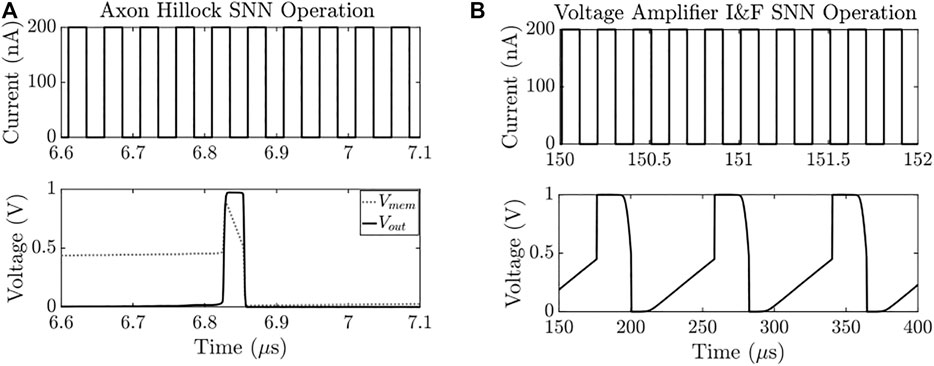
FIGURE 3. Simulation result of (A) Axon Hillock spike generation showing input current (Iin) (top plot), the membrane voltage (Vmem), and the output voltage (Vout) (bottom plot); and (B) voltage amplifier I&F neuron spike generation showing input current (Iin) (top plot and zoomed-in), and the membrane voltage (Vmem) (bottom plot).
2.4.2 Voltage Amplifier I&F Neuron Design
The voltage amplifier I&F circuit (Van Schaik, 2001) (Figure 2B) employs a 5-transistor amplifier that offers better control over the threshold voltage of the neuron. This design allows the designer to determine an explicit threshold and an explicit refractory period. The threshold voltage (Vthr) of the amplifier employed is set to 0.5 V and the VDD is set to 1 V. The neuron membrane is modeled using a 10-pF capacitance (Cmem) and the membrane leakage is controlled by transistor MN4 with a gate (Vlk) voltage of 0.2 V. The excitatory input current spikes (Iin) integrate charge over Cmem and the node voltage at Vmem rises linearly. Once Vmem crosses Vthr, the comparator output switches from “0” to VDD. This output is fed into 2 inverters in series, where the output of the first inverter is used to pull up Vmem to VDD and the output of the second inverter is used to charge a second capacitor (Ck) of 20 pF. The node voltage of Ck is fed back to a reset transistor MN1. When this node voltage is high enough, MN1 is activated and Vmem is pulled down to “0” and remains LOW until Ck discharges below the activation voltage of MN1. For experimental purposes, the input current spikes with an amplitude of 200 nA, a spike width of 25 ns, and a time interval of 25 ns between consecutive spikes is generated through the current source (Iin). Figure 2D depicts the expected results of Vmem. Figure 3B shows the simulation results of input current spikes (Iin) and corresponding membrane voltage (Vout).
2.4.3 SNN Current Driver Design
A current driver provides the input current spikes to the neuron, e.g., image input converted to current spike train. We have designed a current source based on a current mirror (Figure 4A) where VGS of MN2 and MN3 are equal causing both transistors to pass the same current. The sizes of the MN2 and MN3 transistors and the resistor (R1) are chosen to provide a current of amplitude 200 nA. Since the input current of the neuron is modeled as spikes, we have added the MN1 transistor to act as a switch that is controlled by incoming voltage spikes (Vctr) from other neurons.
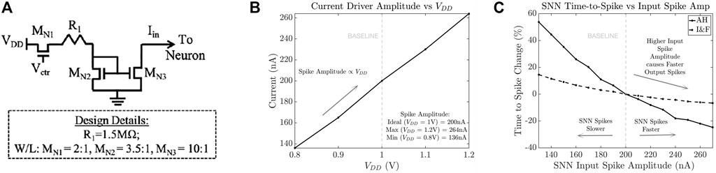
FIGURE 4. (A) Current driver circuit of the SNN neurons with design details; (B) change in current driver output spike (Iin) amplitude with change in VDD; and (C) effect of input spike amplitude on SNN output time-to-spike for Axon Hillock neuron and voltage amplifier I&F neuron.
3 Neuron Attack Models
In this section we describe the power-based attacks and analyze the effect of VDD manipulation on various critical circuit components and parameters of the previously described SNNs.
3.1 Attack Assumptions
We have investigated the power attacks under the following cases:
3.1.1 Case 1: Separate Power Domains
We assume that the current drivers and neurons (of whole SNN) are operated on separate VDD domains. This is possible if the supply voltage of neurons, synapses, and peripherals are distinct, e.g., if the neuron and peripherals are CMOS and the synapses are based on memristors. This case enables us to study the effect of VDD modulation on individual components.
3.1.2 Case 2 Single Power Domain
The entire SNN system, including current drivers and neurons, share the same VDD. This situation is likely if the whole circuit is based on CMOS.
3.1.3 Case 3: Local Power Glitching
The adversary has fine grain control of the VDD inside a voltage domain for both separate and single power domain. For example, adversary can cause local voltage glitching using a focused laser beam.
3.1.4 Case 4: Timed Power Glitching
The adversary controls the time duration of voltage glitching for both separate and single power domains. For example, the adversary modulates the VDD only for a part of the SNN training period. This is a likely scenario for a black box attack where the adversary may not know the internal state of the SNN.
3.2 SNN Input Spike Corruption
The input current spikes of each neuron are fed using a current driver as described in Section 2.4.3. The driver is designed with VDD = 1 V and outputs SNN input current spikes of 200 nA amplitude and 25 ns spike width. An adversary can attack a normal driver operation by modulating the VDD.
Figure 4B shows the effect of modulating the VDD from 0.8 to 1.2 V (corresponding to a −/+ 20% change). The corresponding output spike amplitude ranges from 136 nA for 0.8VDD (−32% change) to 264 nA for 1.2VDD (+32% change). We subjected our neuron designs under these input spike amplitude modulations while keeping the input spiking rate constant at 40 MHz. Figure 4C shows the effect on output spike rate for the Axon Hillock neuron where the time-to-spike (Vout) becomes faster by 24.7% under VDD = 1.2 V and Iin = 264 nA and becomes slower by 53.7% under VDD = 0.8 V and Iin = 136 nA. Similarly, Figure 4C also shows the effect on output spike rate for the voltage amplifier I&F neuron where the time-to-spike (Vout) becomes faster by 6.7% under VDD = 1.2 V and Iin = 264 nA and becomes slower by 14.5% under VDD = 0.8 V and Iin = 136 nA.
3.3 SNN Threshold Manipulation
The adversary can also corrupt normal SNN operation using the externally supplied VDD which can modulate the SNN’s membrane threshold voltage. In the ideal condition, the VDD is 1 V and the threshold voltage of both the Axon Hillock neuron and the I&F neuron are designed to be 0.5 V. Figure 5A shows that the membrane threshold voltage changes with VDD. In the case of the Axon Hillock neuron the change in threshold ranges from −17.91% for VDD = 0.8V to +16.76% for VDD = 1.2V. When VDD is modified, the switching threshold of the inverters in the Axon Hillock neuron is also proportionally affected. A lower (higher) VDD lowers (increases) the switching threshold of the inverters and leads to a faster (slower) output spike. Similarly, the change in threshold ranges from −18.01% to +17.14% when VDD is swept from 0.8 to 1.2 V for the voltage amplifier I&F neuron. Note that the change in threshold for the I&F neuron is due to Vthr signal (Figure 5A) which is derived using a simple resistor-based voltage division of VDD. Therefore, Vthr scales linearly with VDD.
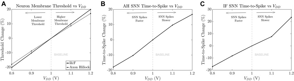
FIGURE 5. (A) Change in SNN membrane threshold with change in VDD; effect of VDD change on SNN output time-to-spike for (B) Axon Hillock neuron; (C) voltage amplifier I&F neuron.
The change in membrane threshold modulates the output spike rate of the affected SNN neurons. Figures 5B,C show the change in time-to-spike under VDD manipulation while the input spikes (Iin) to the neuron are held at a constant amplitude of 200 nA and a rate of 40 MHz. The time-to-spike for the Axon Hillock ranges from 17.91% faster to 16.76% slower. Similarly, the time-to-spike for I&F neuron ranges from 17.05% faster to 23.53% slower.
4 Analysis of Power Attacks on SNN
This section describes the effect of power-oriented attacks on the image classification accuracy under the attack assumptions from Section 3.1.
4.1 Experimental Setup
We have implemented the Diehl and Cook SNN (Diehl et al., 2015) using the BindsNET (Hazan et al., 2018) network library with PyTorch Tensor to test the effect of power-based attacks. The SNN is implemented with 3 neuron layers (Figure 6), namely input layer, excitatory layer (EL), and inhibitory layer (IL). We employ this SNN for digit classification of the MNIST dataset which consists of digit images of pixel dimension 28 × 28. Each input image is converted to Poisson-spike trains and fed to the excitatory neurons in an all-to-all connection, where each input spike is fed to each excitatory neuron. The excitatory neurons are 1-to-1 connected with the inhibitory neurons (Figure 6). Each neuron in the IL is in turn connected to all the neurons in the EL, except the one it received a connection from. The architecture performs supervised learning. For our experiments, the EL and IL have 100 neurons each and all experiments are conducted on 1,000 Poisson-encoded training images with fixed learning rates of 0.000 1 and 0.01 for pre-synaptic and post-synaptic events, respectively. The batch size is set to 32 and training samples are iterated only once as configured in (Hazan et al., 2018). Other key design parameters for the implemented SNN are shown in Table 1. Additional details on the neuron layers, learning method, and SNN parameters can be found in (Hazan et al., 2018). The baseline classification accuracy for attack-free SNN is 75.92% with 60 K training images.
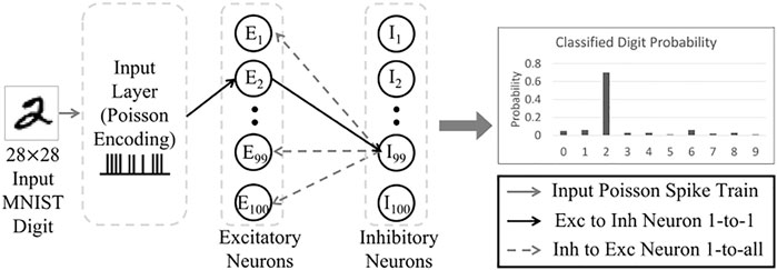
FIGURE 6. Implemented 3-layer SNN (Diehl et al., 2015).
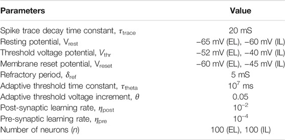
TABLE 1. SNN simulation parameters.
4.2 Input Spike Corruption
In Section 3.2, it is shown that the adversary can manipulate the input spike amplitudes for the SNN neurons. This in turn changes the membrane voltage by a different rate for the same number of input spikes. This manipulation of the rate of change of membrane voltage changes the time-to-spike for the neuron (as shown in Figure 4C).
Attack 1
In order to translate this effect to our BindsNET SNN implementation, we have modified the rate of change of the neuron’s membrane voltage using variable theta which specifies the voltage change in the neuron membrane for each input spike. Figure 7 shows the corresponding change in MNIST digit classification accuracy. Under the worst case theta change of −30%, classification accuracy decreases by 1.9%. Note that this is a white box attack since the adversary requires the location of the current drivers within the SNN (possible by invasive reverse engineering of a chip) to induce the localized fault.
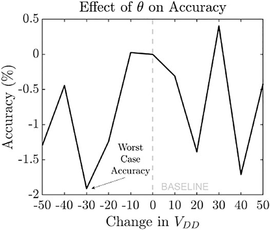
FIGURE 7. Effect of current driver corruption (Attack 1) on MNIST classification accuracy.
4.3 SNN Threshold Manipulation
The key parameters that are used for threshold manipulation are threshold voltage potential (θ0) and membrane reset potential (Vreset). Using our power-based attacks the threshold can be manipulated in two possible ways:
Method 1 (Threshold Range Manipulation)
Table 1 shows that Vthr = −52 mV (EL), −40 mV (IL) and Vreset = −60 mV (EL), −45 (IL). From these values we can calculate that the baseline threshold ranges are 8 mV (EL) and 5 mV (IL), respectively. Using VDD manipulation it is possible to manipulate this threshold range. In Method 1, we manipulate the threshold range of neurons in each layer from −50% to +50% to thoroughly analyze the effects of power attacks in SNN classification tasks.
Method 2 (Threshold Value Manipulation)
Here we leverage the power-based attacks to manipulate only the value of the threshold voltage potential (Vthr). In Section 3.3, it is shown that the adversary can manipulate the membrane threshold voltages of the SNN neurons from −20% to +20% which can affect classification accuracy. The change in threshold value has different effects on neurons from the EL vs. IL. Therefore, we analyze the individual effect of each neuron layer’s on classification accuracy. Finally, we analyze the response for all the layers on the classification accuracy. Note, Attacks 2 to 6 are white box attacks since the adversary requires the location of the individual SNN layers (can be obtained from the layout) to induce the localized faults.
Attack 2
In this attack, we implement Method 1 and subject all the layers of neurons to the same membrane threshold range change. Figure 8A shows the variation in accuracy as 60 K samples are trained with the neuron threshold manipulation. It is seen that the classification accuracy falls as the membrane threshold range of both the layers hits +30% for all periods of training progression. Figure 8A depicts the final average classification accuracy after training 60 K samples under threshold range manipulation. A worst case accuracy degradation of −2.7% below baseline accuracy is observed when the membrane threshold is increased by 30%. The increased threshold range causes a neuron to take longer to build up the membrane potential to fire an output spike. Therefore, the relative spiking time difference (Δt) between 2 connected neurons increases and the corresponding change in synaptic weight (Δw) during each update proportionally decreases. This, in turn, means that SNN with higher threshold ranges would require longer (more training) to achieve the same accuracy as SNN with smaller threshold ranges.
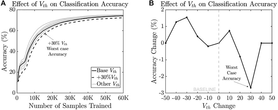
FIGURE 8. (A) Progression of classification accuracy for 60 K training samples under threshold range variation; and (B) final classification accuracy for various Vth showing worst-case degradation (Attack 2).
Attack 3
In this case, we subject only the EL to membrane Method 2 threshold variation to study its individual effect on classification accuracy. This attack is possible when (1) each neuron layer has their own voltage domain and the adversary injects a laser-induced fault, (2) neuron layers share voltage domain but the local fault injection in one layer does not propagate to other layers due to the capacitance of the power rail. Various fraction of neurons in this layer, ranging from 0 to 100% are subject to -20% to +20% threshold change This analysis is performed to model the situation when an adversary has fine grain control of the VDD inside a voltage domain, e.g., using local voltage glitching attack that affects only a section of neurons. This is possible in systems that have thousands of neurons per layer that may be physically isolated due to interleaving synapse arrays. Figure 9A shows the corresponding change in the classification accuracy. It is noted that classification accuracy is equal to or better than the baseline accuracy for threshold changes as long as ≤ 90% of the layer is affected. For the worst case threshold change of −20%, the classification accuracy degrades by 7.32% when 100% of the EL is affected. In summary, attacking the EL alone has a relatively low impact on the output accuracy. This is intuitive since the effect of any corruption in the EL can be recovered in the following IL.
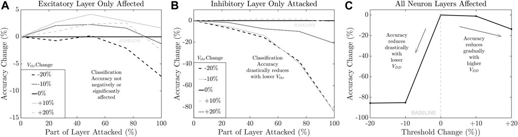
FIGURE 9. Classification accuracy trend with SNN membrane threshold for (A) excitatory layer only (Attack 3); (B) inhibitory layer only (Attack 4); and (C) both excitatory layer and inhibitory layer (Attack 5).
Attack 4
In this attack, we subject only the IL to the membrane threshold change. Various fraction of neurons in this layer ranging from 0 to 100% are subject to −20% to +20% threshold change. Figure 9B shows the corresponding change in classification accuracy. It is noted that classification accuracy degrades below the baseline accuracy for 3 out of 4 cases of threshold change and for all fractions of IL affected. A worst-case degradation of 84.52% below the baseline accuracy (observed at −20% threshold change at 100% of IL affected) is noted. In summary, attacking the IL has a more significant effect on output accuracy compared to attacking the EL alone. This is understandable since IL is the final layer before the output. Therefore, any loss in learning cannot be recovered.
Attack 5
In this attack, we subject 100% of both the EL and the IL to the same membrane threshold change. Figure 9C shows the variation in accuracy with the threshold for both the layers of neurons. It is seen that the classification accuracy falls sharply as the membrane threshold of both the layers decreases below the baseline. A worst case accuracy degradation of −85.65% below baseline accuracy is observed when the membrane threshold is reduced by 20%.
Attack 6
In this attack, we vary the timing of threshold manipulation. We consider the worst-case threshold corruption for the three cases of EL only, IL only, and EL + IL for various time duration ranging from 0 to 100% of the training phase. Figures 10A–C show the corresponding effect on the classification accuracy. While maximum accuracy degradation is observed when 100% of the training phase is affected, timed attacks for even 25% of the training phase show accuracy degradation of 32% (EL + IL), 30% (IL only), and 28% (EL only).
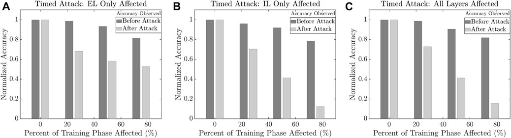
FIGURE 10. Classification accuracy trend during timed threshold manipulation (Attack 6) of (A) excitatory layer only; (B) inhibitory layer only; and (C) both excitatory layer and inhibitory layer.
4.4 Input Spike Corruption and Threshold Manipulation
Attack 7
This is a black box attack where the adversary does not need to know the internal architecture of the current driver or the SNN neurons. Here we assume that the power supply is shared among all the components of the SNN system, including the current drivers and all of the neuron layers. Manipulating the VDD changes both membrane voltage per spike (theta) and the threshold voltages (Vthr) (Method 1) of the SNN neurons. Figure 11 shows that the worst case accuracy degradation is −84.93%.
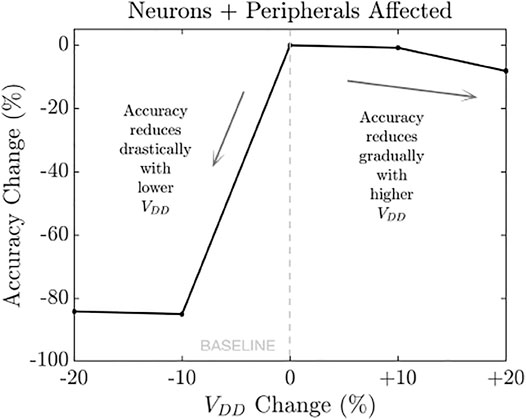
FIGURE 11. Change in classification accuracy with VDD change for entire system (neurons and peripherals) (Attack 7).
4.5 Summary of Power Attack Analysis
From our analysis, we conclude following:
4.5.1 SNN Assets
These include: (1) spike rate and amplitude, (2) neuron membrane threshold, and (3) membrane voltage change per spike. Other assets (not studied in this paper) are strength of synaptic weights between neurons and the SNN learning rate.
4.5.2 SNN Vulnerabilities
VDD manipulation (1) generation of spikes of lower/higher amplitude than nominal value by the neuron’s input current driver, (2) lowers/increases neuron’s membrane threshold. Both vulnerabilities cause affected neurons to spike faster/slower.
4.5.3 Attack Models
Manipulation of global and local fine-grained power supply corrupts critical training parameters. Attacks not covered in this paper are (1) generation of adversarial input samples to cause misclassification, (2) fault injection into synaptic weights, and (3) noise injection in input samples to attack specific neurons.
5 Defenses Against Power-Based SNN Attacks
In Section 2.3, the learning rule for the implemented architecture is explained. The three key designer-controlled parameters include the post- and pre-synaptic learning rates (ηpre/ηpost), the spike trace decay time constant (τt), and the number of neurons (n) used per layer. In this section, we analyze the effect of these parameters on SNN classification accuracy under the fault-free (i.e., baseline) and faulty conditions. The STDP parameters can be tuned by modifying the shape of the pre- and post-synaptic spikes as shown in (Saudargiene et al., 2004). These defenses that use design choices (in section 5.1–5.3) are effective against Attack 1 and Attack 2 where the accuracy degradation is caused due to input spike corruption and threshold range manipulation. Furthermore, we propose multiple circuit-level modifications and logic additions (in Section 5.4–5.6) that defend against all proposed attacks (Attack 1–7).
5.1 Impact of STDP Synaptic Learning Rate
The baseline synaptic learning rates of the SNN implemented (shown in Table 1) are 10–2 and 10–4 for ηpost and ηpre, respectively. We subject the neurons in the implemented SNN with adversarial threshold range variation of −50% to +50%. The learning rates of the SNN is varied by
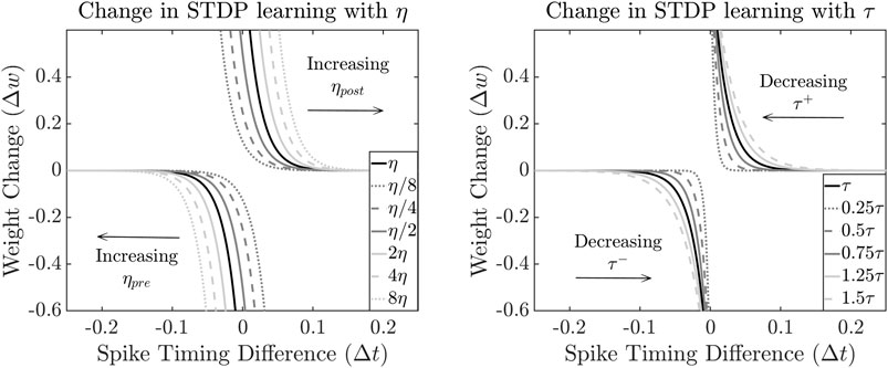
FIGURE 12. Change in STDP learning curve with (A) learning rate (η); and (B) trace decay constant (τ).
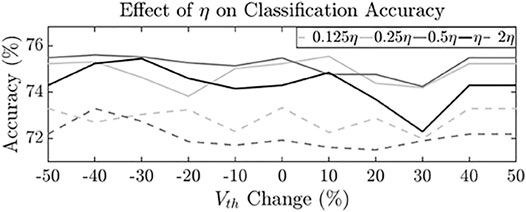
FIGURE 13. Effect of learning rate (η) on MNIST classification accuracy after training 60 K samples under adversarial threshold variation.
5.2 Impact of STDP Synaptic Trace Decay Constant
The baseline synaptic trace decay constant (τ) (Table 1) is 20 ms. We vary τ from 0.25X to 1.5X under our adversarial power attack to determine its effect on classification accuracy. Figure 12B shows that increasing (decreasing) τ causes a shallower (steeper) slope to the STDP curve and correspondingly a lower (higher) change in synaptic weight (Δw) for the same spike timing difference (Δt). Figure 14 shows the final average classification accuracy after training the SNN with 60 K samples under different τ and threshold (Vth) values. It is seen that the highest accuracy is observed for SNN with trace decay constant of 0.25τ which improves average classification accuracy by 0.81%. The lowest accuracy is observed for SNN with trace decay constant of 1.25τ which further degrades classification accuracy by −0.26%. Lowering the trace decay constant causes a steeper STDP curve and effectively reduces the window of spike timing difference (Δt) within which the synaptic weights are updated. Therefore, lowering the frequency of updates correspondingly minimizes the effect of power-based attacks on STDP learning. Similarly, increasing τ causes a wider update window and leads to a more pronounced effect on final classification accuracy. For Attack 1 and 2, where accuracy loss of 1.9 and 2.7% is observed, this method recovers accuracy degradation by 42 and 30%, respectively.
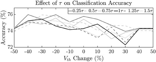
FIGURE 14. Change in STDP learning curve with trace decay constant (τ).
5.3 Impact of Number of Neurons per Layer
In the baseline SNN implementation, we utilized 100 neurons (n) in the IL and EL each. We increase the range of neurons per layer to include n = 50, 150, 225, and 400 to study its effect on classification accuracy under adversarial threshold variation. Figure 15 shows the final classification accuracy observed under different n and Vth. Ideally, a greater number of neurons increases the classification accuracy. Here we see that n = 150 maximizes the accuracy under most of the Vth cases and improves average classification accuracy by 0.94%. Further increasing n to 225 and 400 leads to a degradation in accuracy. The worst case is observed when n = 400, where the average accuracy degrades by 17.18%. This can be attributed to the fact that a higher number of neurons under attack have a more pronounced negative effect on SNN training. Ideally, the designer should increase n only up to a point where the increase in output accuracy caused by a higher n is greater than the accuracy degradation faced by a greater number of neurons under attack. For Attack 1 and 2, where accuracy loss of 1.9 and 2.7% is observed, this method recovers accuracy degradation by 47 and 34%, respectively.
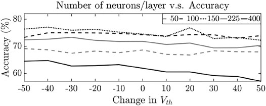
FIGURE 15. Impact on number of neurons per SNN layer on classification accuracy under adversarial Vth manipulation.
5.4 Robust Current Driver Design
We propose a current driver that produces neuron input spikes of constant amplitude (Figure 16A). Here the negative input terminal of the op-amp is forced to a reference voltage that leads the positive terminal to be virtually connected to the reference voltage (VRef). The current through MP1 transistor is VRef/R1 and the negative feedback of the amplifier forces the gate voltage of MP1 to satisfy the current equation of the transistor. Since VGS and Vth of MP1 and MP2 transistors are the same, MP2 passes the same current as MP1. Note, we have used long channel transistors to reduce the effect of channel length modulation. The power overhead incurred for the proposed robust current driver compared to the unsecured version is 3%. Note that the area overhead of the robust driver is negligible compared to the area of unsecured driver since the neuron capacitors occupy the majority of the area.
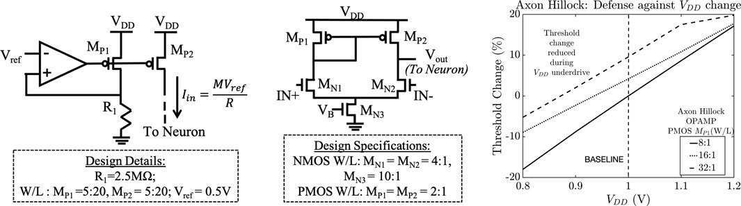
FIGURE 16. (A) Robust SNN current driver (constant output spike amplitude); (B) comparator designed and implemented in the Axon Hillock neuron to mitigate threshold variation.
5.5 Resiliency to Threshold Voltage Variation
5.5.1 Voltage Amplifier I&F Neuron
In order to prevent Vthr from being corrupted due to VDD change, it can be generated using a bandgap voltage reference that produces a constant voltage irrespective of power and temperature variations. A bandgap circuit is proposed in (Sanborn et al., 2007) that generates a constant Vref signal with an output variation of ± 0.56% for supply voltages ranging from 0.85 to 1 V at room temperature. A similar design can be used for our proposed I&F neuron that requires a constant external Vthr signal. Since the Vthr variation (±0.56%) under VDD manipulation is negligible, the classification accuracy degradation reduces to ∼0%. For our experimental 100-neuron (per layer) implementation, the area overhead incurred by the bandgap circuit is 65%. But this can be significantly reduced if the bandgap circuit is shared with other components of the chip and if the SNNs are implemented with tens of thousands of neurons as required by various applications.
5.5.2 Axon Hillock Neuron
Comparator implementation
We replace the first inverter in the Axon Hillock neuron with a comparator that employs Vthr generated by a bandgap circuit (Sanborn et al., 2007) as the reference voltage to eliminate the effect of VDD variation on the inverter switching threshold. The rest of the design remains the same. Figure 16B shows the implemented comparator which ensures that the threshold voltage is not determined by the sizing of the inverter transistors or the VDD. Instead, it depends on the input biasing of the proposed design. The IN+ and IN- bias is set to 600 mV and VB is set to 400 mV. The power overhead incurred is 11% and the area overhead is negligible since the 1 pF capacitors occupy a majority of the neuron area.
Neuron transistor sizing
In the case of the Axon Hillock neuron (Figure 2A), the membrane threshold is determined by the VDD and the design of the first inverter (transistors MP1 and MN3). Simulations indicate that classification accuracy is affected mostly by lowering the membrane threshold as shown in Figure 9C. We increased the sizing of the PMOS transistor MP1 to limit the threshold change due to VDD. Figure 16C shows that increasing the W/L ratio mitigates the reduction in threshold changes under lower VDD. At 0.8 V, the threshold change observed for W/L ratio of 32:1 is −5.23% compared to −18.01% for the baseline sizing. The corresponding degradation in classification accuracy at VDD = 0.8V is only 3.49% which is a significant improvement compared to the 85.65% degradation observed previously. At VDD = 1.2V, the threshold change increases by 3.2% for W/L ratio of 32:1 and the corresponding accuracy degradation only increases by 1.4%. For the upsized neuron, the power overhead observed is 25% while the area overhead is negligible since the majority of the neuron area is occupied by the two 1 pF capacitors that remain unchanged in the new design.
5.6 Detection of VDD Manipulation
In addition to robust neuron design, we also propose a technique to voltage glitching attack directed at an individual neuron layer. This is done by introducing a dummy neuron within each neuron layer (shown in Figure 17A). In our design, the input of the dummy neuron is connected to a current driver that constantly drives spiking inputs of 200 nA amplitude and spike width of 100 ns. The spikes repeat every 200 ns and do not depend on the spiking of the neurons from the previous layer. Under ideal conditions, the number of output spikes for a fixed sampling period for each dummy neuron should be identical. Figure 17B shows the effect of VDD change on the dummy neuron’s output for both the I&F and AH neurons over a sampling period of 100 ms. It is seen that for both neurons, the number of dummy output spikes differs by
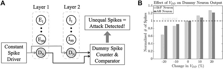
FIGURE 17. (A) VDD change detection using dummy neuron; and (B) effect of VDD on dummy neuron output.
6 Discussion
6.1 Extension to Other Neuromorphic Materials
In this study, we have analyzed the impact of power-based attacks on integrate-and-fire CMOS-based neurons, that are most commonly employed for contemporary SNN architectures. But each CMOS-based neuron requires tens of transistors and therefore incurs a large area and a high power consumption. Neurons based on emerging technology such as memristors, ferroelectric devices, and phase change memories can address the above challenges. Integrate-and-fire neurons using memristors have been proposed (Mehonic and Kenyon, 2016) and (Lashkare et al., 2018) where short voltage pulses (input spikes) are employed to increase the conductance of the memristor device. When the conductance reaches a critical value (threshold), the neuron fires a spike, and the conductance is reset. Varying the supply voltage would cause the amplitude of the input spikes to increase/decrease and correspondingly cause the neuron to fire faster/slower. Once the neuron fires, the conductance is reset using a reset pulse that is also VDD dependent. Varying the supply voltage would also lead to improper reset operation. Multiple works (Mulaosmanovic et al., 2018; Chen et al., 2019; Dutta et al., 2019) have proposed ferroelectric devices for neuromorphic computing. In (Mulaosmanovic et al., 2018) a controlled electric field is applied to reversibly tune the polarization state of the ferroelectric material. When a series of short voltage pulses are applied consecutively, it causes an incremental nucleation of nanodomains in the ferroelectric layer. When a critical number of nanodomains are nucleated, it leads to an abrupt polarization reversal which corresponds to the neuron firing. It is shown that the rate of nucleation depends on the amplitude and duration of the input voltage pulses. Therefore, the proposed power-based attacks can corrupt the spiking rate and inject faults in ferroelectric neurons as well. In the case of phase change memories (PCM), the effective thickness of the amorphous region of the chalcogenide can be considered equivalent to the membrane potential of a neuron. In (Sebastian et al., 2014; Tuma et al., 2016), it is shown that the amorphous region can be grown precisely by controlling the input voltage pulse. Consecutive voltage pulses can allow controlled crystallization and ultimately leads to an abrupt change in PCM conductance which corresponds to the neuron firing. It is also shown that the firing rate of the PCM neurons can be controlled by manipulating the amplitude of the voltage pulses. Therefore, our power-based attacks can corrupt the spiking rate and inject faults in PCM-based neurons as well.
6.2 Extension to Other Neural Network Architectures
Although this work analyzes the impact of power-based fault injection attacks on SNNs, these attacks can be extended to other NNAs as well. Very limited research has been conducted on physical attacks (i.e., power-based) on traditional NNAs res such as DNNs. In (Breier et al., 2018) and (Hou et al., 2020), the authors study physical fault injection attacks into the hidden layers of DNNs using laser injection techniques to demonstrate image misclassification. In (Benevenuti et al., 2018), the authors characterize each network layer of an ANN under a laser beam by placing them separately on an FPGA floorplan. The authors demonstrate significant degradation in classification accuracy under these laser-based attacks. The proposed power-based attacks can be extended to other types of ANNs by analyzing the effect of VDD variation on the operation of neurons. The ANN can then be implemented with these neurons under attack and the corresponding accuracy change due to their faulty behavior can be determined. This analysis can be the subject of future study.
7 Conclusion
We propose one black box and six white box attacks against commonly implemented SNN neuron circuits by manipulating its external power supply or inducing localized power glitches. We have demonstrated power-oriented corruption of critical SNN training parameters. We introduced the attacks for SNN-based digit classification tasks as test cases and observed significant degradation in classification accuracy. We analyzed defenses techniques that leverage various SNN design parameters (such as learning rate, trace decay constant, and number of neurons) to mitigate accuracy degradation due to power-based attacks. Finally, we also proposed hardware modifications and additions to SNNs (such as robust current driver design and VDD manipulation detection) as countermeasures to our proposed power-based attacks.
Data Availability Statement
The original contributions presented in the study are included in the article/Supplementary Material. Further inquiries can be directed to the corresponding author.
Author Contributions
KN: Implemented hardware SNN neurons, introduced fault injection attacks, simulated Python implementation of SNN, generated results, plots, and designed all the schematics. JL: Helped with Python implementation of SNN and ran simulations. SE: Helped with developing hardware defenses against SNN power attacks. SK: Contributed in overall idea evaluation, discussion, and threat model creation. SG: Contributed in overall idea evaluation, problem identification, write-up, design debug, and result generation.
FUNDING
This work is supported by SRC (2847.001 and 3011.001) and NSF (CNS-1722557, CCF-1718474, DGE-1723687, DGE-1821766, OIA-2040667 and DGE-2113839).
Conflict of Interest
SK was employed by the company Ampere Computing.
The remaining authors declare that the research was conducted in the absence of any commercial or financial relationships that could be construed as a potential conflict of interest.
Publisher’s Note
All claims expressed in this article are solely those of the authors and do not necessarily represent those of their affiliated organizations, or those of the publisher, the editors, and the reviewers. Any product that may be evaluated in this article, or claim that may be made by its manufacturer, is not guaranteed or endorsed by the publisher.
References
Azghadi, M. R., Lammie, C., Eshraghian, J. K., Payvand, M., Donati, E., Linares-Barranco, B., et al. (2020). Hardware Implementation of Deep Network Accelerators towards Healthcare and Biomedical Applications. IEEE Trans. Biomed. Circuits Syst. 14, 1138–1159. doi:10.1109/tbcas.2020.3036081
Bagheri, A., Simeone, O., and Rajendran, B. (2018). “Adversarial Training for Probabilistic Spiking Neural Networks,” in 2018 IEEE 19th International Workshop on Signal Processing Advances in Wireless Communications (SPAWC), Kalamata, Greece, June 25–28, 2018 (IEEE), 1–5. doi:10.1109/spawc.2018.8446003
Barenghi, A., Breveglieri, L., Koren, I., and Naccache, D. (2012). Fault Injection Attacks on Cryptographic Devices: Theory, Practice, and Countermeasures. Proc. IEEE 100, 3056–3076. doi:10.1109/jproc.2012.2188769
Benevenuti, F., Libano, F., Pouget, V., Kastensmidt, F. L., and Rech, P. (2018). “Comparative Analysis of Inference Errors in a Neural Network Implemented in Sram-Based Fpga Induced by Neutron Irradiation and Fault Injection Methods,” in 2018 31st Symposium on Integrated Circuits and Systems Design (SBCCI), Bento Goncalves, RS, August 27–31, 2018 (IEEE), 1–6. doi:10.1109/sbcci.2018.8533235
Bozzato, C., Focardi, R., and Palmarini, F. (2019). Shaping the Glitch: Optimizing Voltage Fault Injection Attacks. Tches 2019 (2), 199–224. doi:10.46586/tches.v2019.i2.199-224
Breier, J., Hou, X., Jap, D., Ma, L., Bhasin, S., and Liu, Y. (2018). “Practical Fault Attack on Deep Neural Networks,” in Proceedings of the 2018 ACM SIGSAC Conference on Computer and Communications Security, Toronto, Canada, October 15–19, 2018, 2204–2206. doi:10.1145/3243734.3278519
Cao, Y., Chen, Y., and Khosla, D. (2015). Spiking Deep Convolutional Neural Networks for Energy-Efficient Object Recognition. Int. J. Comput. Vis. 113, 54–66. doi:10.1007/s11263-014-0788-3
Chen, C., Yang, M., Liu, S., Liu, T., Zhu, K., Zhao, Y., et al. (2019). “Bio-inspired Neurons Based on Novel Leaky-Fefet with Ultra-low Hardware Cost and Advanced Functionality for All-Ferroelectric Neural Network,” in 2019 Symposium on VLSI Technology, Kyoto, Japan, June 9–14, 2019 (IEEE), T136–T137. doi:10.23919/vlsit.2019.8776495
Davies, M., Srinivasa, N., Lin, T.-H., Chinya, G., Cao, Y., Choday, S. H., et al. (2018). Loihi: A Neuromorphic Manycore Processor with On-Chip Learning. Ieee Micro 38, 82–99. doi:10.1109/mm.2018.112130359
Diehl, P. U., Neil, D., Binas, J., Cook, M., Liu, S.-C., and Pfeiffer, M. (2015). “Fast-classifying, High-Accuracy Spiking Deep Networks through Weight and Threshold Balancing,” in 2015 International joint conference on neural networks (IJCNN), Killarney, Ireland, July 11–16, 2015 (IEEE), 1–8. doi:10.1109/ijcnn.2015.7280696
Dutta, S., Saha, A., Panda, P., Chakraborty, W., Gomez, J., Khanna, A., et al. (2019). “Biologically Plausible Ferroelectric Quasi-Leaky Integrate and Fire Neuron,” in 2019 Symposium on VLSI Technology, Kyoto, Japan, June 9–14, 2019 (IEEE), T140–T141. doi:10.23919/vlsit.2019.8776487
Goodfellow, I. J., Shlens, J., and Szegedy, C. (2014). Explaining and Harnessing Adversarial Examples. preprint arXiv:1412.6572.
Hazan, H., Saunders, D. J., Khan, H., Patel, D., Sanghavi, D. T., Siegelmann, H. T., et al. (2018). Bindsnet: A Machine Learning-Oriented Spiking Neural Networks Library in python. Front. Neuroinform. 12, 89. doi:10.3389/fninf.2018.00089
Heiberg, T., Kriener, B., Tetzlaff, T., Einevoll, G. T., and Plesser, H. E. (2018). Firing-rate Models for Neurons with a Broad Repertoire of Spiking Behaviors. J. Comput. Neurosci. 45, 103–132. doi:10.1007/s10827-018-0693-9
Hou, X., Breier, J., Jap, D., Ma, L., Bhasin, S., and Liu, Y. (2020). “Security Evaluation of Deep Neural Network Resistance against Laser Fault Injection,” in 2020 IEEE International Symposium on the Physical and Failure Analysis of Integrated Circuits (IPFA), Singapore, July 20–23, 2020 (IEEE), 1–6. doi:10.1109/ipfa49335.2020.9261013
Indiveri, G., Linares-Barranco, B., Hamilton, T. J., Schaik, A. v., Etienne-Cummings, R., Delbruck, T., et al. (2011). Neuromorphic Silicon Neuron Circuits. Front. Neurosci. 5, 73. doi:10.3389/fnins.2011.00073
Kaiser, J., Tieck, J. C. V., Hubschneider, C., Wolf, P., Weber, M., Hoff, M., et al. (2016). “Towards a Framework for End-To-End Control of a Simulated Vehicle with Spiking Neural Networks,” in 2016 IEEE International Conference on Simulation, Modeling, and Programming for Autonomous Robots (SIMPAR), San Francisco, CA, December 13–16, 2016 (IEEE), 127–134. doi:10.1109/simpar.2016.7862386
Kurakin, A., Goodfellow, I., Bengio, S., et al. (2016). Adversarial Examples in the Physical World. [arXiv preprint arXiv:1607.02533].
Lashkare, S., Chouhan, S., Chavan, T., Bhat, A., Kumbhare, P., and Ganguly, U. (2018). Pcmo Rram for Integrate-And-Fire Neuron in Spiking Neural Networks. IEEE Electron. Device Lett. 39, 484–487. doi:10.1109/led.2018.2805822
Maass, W. (1997). Networks of Spiking Neurons: the Third Generation of Neural Network Models. Neural networks 10, 1659–1671. doi:10.1016/s0893-6080(97)00011-7
Madry, A., Makelov, A., Schmidt, L., Tsipras, D., and Vladu, A. (2017). Towards Deep Learning Models Resistant to Adversarial Attacks. preprint arXiv:1706.06083.
Marchisio, A., Nanfa, G., Khalid, F., Hanif, M. A., Martina, M., and Shafique, M. (2020). “Is Spiking Secure? a Comparative Study on the Security Vulnerabilities of Spiking and Deep Neural Networks,” in 2020 International Joint Conference on Neural Networks (IJCNN), Glasgow, UK, July 19–24 July, 2020 (IEEE), 1–8.
Mead, C., and Ismail, M. (2012). Analog VLSI Implementation of Neural Systems, 80. Springer Science & Business Media.
Mehonic, A., and Kenyon, A. J. (2016). Emulating the Electrical Activity of the Neuron Using a Silicon Oxide Rram Cell. Front. Neurosci. 10, 57. doi:10.3389/fnins.2016.00057
Merolla, P. A., Arthur, J. V., Alvarez-Icaza, R., Cassidy, A. S., Sawada, J., Akopyan, F., et al. (2014). A Million Spiking-Neuron Integrated Circuit with a Scalable Communication Network and Interface. Science 345, 668–673. doi:10.1126/science.1254642
Mulaosmanovic, H., Chicca, E., Bertele, M., Mikolajick, T., and Slesazeck, S. (2018). Mimicking Biological Neurons with a Nanoscale Ferroelectric Transistor. Nanoscale 10, 21755–21763. doi:10.1039/c8nr07135g
Sanborn, K., Ma, D., and Ivanov, V. (2007). A Sub-1-v Low-Noise Bandgap Voltage Reference. IEEE J. Solid-state Circuits 42, 2466–2481. doi:10.1109/jssc.2007.907226
Saudargiene, A., Porr, B., and Wörgötter, F. (2004). How the Shape of Pre- and Postsynaptic Signals Can Influence STDP: A Biophysical Model. Neural Comput. 16, 595–625. doi:10.1162/089976604772744929
Sebastian, A., Le Gallo, M., and Krebs, D. (2014). Crystal Growth within a Phase Change Memory Cell. Nat. Commun. 5, 4314–4319. doi:10.1038/ncomms5314
Tavanaei, A., Ghodrati, M., Kheradpisheh, S. R., Masquelier, T., and Maida, A. (2019). Deep Learning in Spiking Neural Networks. Neural Networks 111, 47–63. doi:10.1016/j.neunet.2018.12.002
Tuma, T., Pantazi, A., Le Gallo, M., Sebastian, A., and Eleftheriou, E. (2016). Stochastic Phase-Change Neurons. Nat. Nanotech 11, 693–699. doi:10.1038/nnano.2016.70
Van Schaik, A. (2001). Building Blocks for Electronic Spiking Neural Networks. Neural networks 14, 617–628. doi:10.1016/s0893-6080(01)00067-3
Venceslai, V., Marchisio, A., Alouani, I., Martina, M., and Shafique, M. (2020). “Neuroattack: Undermining Spiking Neural Networks Security through Externally Triggered Bit-Flips,” in 2020 International Joint Conference on Neural Networks (IJCNN), Glasgow, UK, July 19–24 (IEEE), 1–8. doi:10.1109/ijcnn48605.2020.9207351
Whatmough, P. N., Lee, S. K., Brooks, D., and Wei, G.-Y. (2018). Dnn Engine: A 28-nm Timing-Error Tolerant Sparse Deep Neural Network Processor for Iot Applications. IEEE J. Solid-state Circuits 53, 2722–2731. doi:10.1109/jssc.2018.2841824
Zussa, L., Dutertre, J.-M., Clediere, J., and Tria, A. (2013). “Power Supply Glitch Induced Faults on Fpga: An In-Depth Analysis of the Injection Mechanism,” in 2013 IEEE 19th International On-Line Testing Symposium (IOLTS), Chania, Greece, July 8–10, 2013 (IEEE), 110–115. doi:10.1109/iolts.2013.6604060
Keywords: spiking neural network, security, fault injection, STDP, side channel attack
Citation: Nagarajan K, Li J, Ensan SS, Kannan S and Ghosh S (2022) Fault Injection Attacks in Spiking Neural Networks and Countermeasures. Front. Nanotechnol. 3:801999. doi: 10.3389/fnano.2021.801999
Received: 26 October 2021; Accepted: 30 November 2021;
Published: 11 January 2022.
Edited by:
Ying-Chen (Daphne) Chen, Northern Arizona University, United StatesReviewed by:
Jayasimha Atulasimha, Virginia Commonwealth University, United StatesYao-Feng Chang, Intel, United States
Copyright © 2022 Nagarajan, Li, Ensan, Kannan and Ghosh. This is an open-access article distributed under the terms of the Creative Commons Attribution License (CC BY). The use, distribution or reproduction in other forums is permitted, provided the original author(s) and the copyright owner(s) are credited and that the original publication in this journal is cited, in accordance with accepted academic practice. No use, distribution or reproduction is permitted which does not comply with these terms.
*Correspondence: Karthikeyan Nagarajan, kxn287@psu.edu