Editorial: Advanced opto-electrical modeling of photovoltaic materials and devices
 Janez Krc
 Martina Schmid
 Rudi Santbergen
- 1Faculty of Electrical Engineering, University of Ljubljana, Ljubljana, Slovenia
- 2University of Duisburg-Essen, Duisburg, Germany
- 3Delft University of Technology, Delft, Netherlands
Editorial on the Research Topic
Advanced opto-electrical modeling of photovoltaic materials and devices
Research and innovation in photovoltaic (PV) materials and devices have been expanding over the last decades, aiming at continuously improved performance and broadened applications. Thus, the strive for new solutions and the motivation to design, analyze and test new solutions and concepts is growing. In this respect, modeling and simulations play a central role in the entire chain of photovoltaic research and development, including materials, devices, and systems. Computer simulation can replace time-consuming experimental parameter variations and testing, when searching for optimized materials and device configurations. Furthermore, they enable to perform comprehensive analyses and contribute to physical insight into material properties and device or system operation. Modeling and simulations also present a strong predictive tool.
The models used for PV material and device simulations should account for optical and electrical properties. Careful optical design and optimization of state-of-the-art solar cells and PV modules require advanced modeling approaches to be used, taking into account multilayer stacks of thin coherent and thick incoherent layers and nano, micro, or macro photonic structures for efficient light coupling and trapping. Design and simulation of improved concentrating optical systems also play an important role. Optical modeling of luminescent materials, which are incorporated inside the device structures to tailor the frequency spectrum of light for improved absorption is of importance. Tandem devices, including emerging wide bandgap materials, such as perovskites, are researched intensively. These examples clearly show the need for a variety of optical models to be included or developed for efficient and accurate optical simulations. Optical models are further combined with electrical ones to perform the complete opto-electrical simulations of PV materials and devices. Electronic characteristics of materials and interfaces have to be included in electrical models to properly describe charge carrier transport in layers and at interfaces of multilayer structures of solar cells. Moreover, materials incorporating nanostructures such as quantum dots and quantum wells need to be addressed adequately in electrical models.
Advanced optical and opto-electrical modeling and simulations of PV materials and devices are the research topic of this Research Topic. The Research Topic consists of five original scientific contributions. The papers are mainly focused on device modeling and simulations, however, they also include elements of material modeling and characterization. The first three papers are dedicated to optical modeling and simulations of solar cells, whereas the last two papers include both, optical and electrical modeling and simulations. Let us give a brief introduction to the research contents of the papers. In the paper of Hägglund a new optical model for simulations of tandem devices, in particular perovskite/silicon solar cells, including both, micro and nanostructures for light manipulation, is presented. In the next paper, Kovacic et al. present optical simulation results of the analysis of incorporating laser-reduced graphene oxide layers in the structure of perovskite/Cu(In,Ga)Se2 solar cells. In the paper of Eisler et al. the authors research the advantage of the extraordinary optical properties afforded by nanophotonic structures to create a photonic luminescent solar concentrator for an InGaP-Si multijunction concentrator solar cell. In the paper of Aeberhard et al. a full opto-electronic device simulation on continuum level, using a hopping model for the explicit description of the charge recombination junction, is presented. In the paper of Heerden et al. the authors perform the simulation study of the origin of hysteretic behavior of current-voltage characteristics of perovskite solar cells and reveal that the density of shallow defects at the interfaces between perovskite and transport layers play a key role in the hysteresis phenomena.
With this Research Topic, we aim at highlighting the importance of numerical modeling and simulations of PV devices. We wish that it will motivate researchers to use the power of modeling and simulations in their own work.
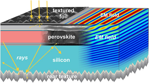
Multiscale Optical Modeling of Perovskite-Si Tandem Solar Cells Hägglund. Uppsala University, Uppsala, Sweden with the success of silicon (Si) solar cell technology, research and development on higher efficiency multijunction solar cells is gaining much attention. Tandem cells with a perovskite top cell and a Si bottom cell show particular potential. However, the optical modeling of such devices is complicated by the broad range of length scales involved; the optically thin layers and nanoscale features of a perovskite solar cell require some version of wave optics or even full field electromagnetic (EM) calculations, while the micrometer scale structuring and large dimensions of Si cells are much more manageable using geometrical (ray) optics. In the present work, a method for combining EM and ray optical calculations is developed and described in detail, with an example provided in the software Comsol Multiphysics. For regions with thin films or nanoscale features, EM wave calculations are performed using the finite element method. These calculations provide the phase and amplitude of the waves refracted and reflected into different diffraction orders, of which only the regular reflection and transmission are typically of relevance for nanoscale periodicity. In the ray optics simulation, the corresponding regions are implemented as diffracting interfaces, with deterministic transformations of the Stokes vector components according to the EM wave calculations. Meanwhile, the absorbed intensity of interacting rays are recorded. The method is applied to separate perovskite and Si solar cells and to a few tandem solar cells of relevance for two-versus four-terminal configurations. Corrections for strongly absorbing media in the ray tracing algorithm, which use generalized versions of the Fresnel coefficients, Snell’s law and the Beer-Lambert law, are also evaluated. In a typical Si solar cell with a front surface structure of inverted pyramids, the correction is found to reduce the absorption by up to 0.5 percentage units compared to a conventional ray tracing calculation. The difference is concluded to originate mainly from reduced absorption rates of inhomogeneous waves, rather than from enhanced escape rates of (quasi-) trapped rays at the Si front surface.
Optical simulation study of perovskite/CIGS tandem solar cells with reduced graphene oxide layers Kovacic et al. Tandem solar cells present a promising solution to overcome the Schottky-Queisser efficiency limit of single-junction solar cells. In this paper an all-thin-film tandem solar cell based on perovskite (PK) top cell and chalcopyrite Cu(In, Ga)Se2 (CIGS) bottom cell is researched. Device optical simulations are validated on the top and bottom cell separately and employed to investigate optical effects of introduced laser-reduced graphene oxide (rGO) layers at two positions in the tandem cell, namely on top of PK cell underneath the front transparent electrode and at the position between the top PK and bottom CIGS cell. The purpose of introduced rGO layers is to improve optoelectrical properties of the device, based on tunable electronic and optical characteristics of rGO layers. Optical simulation results show that the parasitic absorption in rGO layers may noticeably affect the performance of the tandem cell if the layers are not optimized. The use of very thin (a few nm) rGO is suggested from the analysis if the parasitic absorption of layers is not reduced. Directions for further optimization of optical rGO, including reduction of parasitic absorption and tuning of the real part of refractive index is performed.
Photonic Luminescent Solar Concentrator Design for High Efficiency, Low Cost Multijunction Photovoltaics Eisler et al. despite the extraordinary advances in solar cell efficiency in laboratory settings, the deployment of solar cells continues to be limited to low efficiency (<25%) silicon cells because of cost. In this work, we take advantage of the extraordinary optical properties afforded by nanophotonic structures to create a photonic luminescent solar concentrator for an InGaP-Si multijunction concentrator cell. Finite difference time domain (FDTD) simulations demonstrated a concentrator that could effectively capture, downconvert, and guide concentrated light to an InGaP subcell while still transmitting longer wavelengths to a Si subcell. We fabricated the photonic luminescent solar concentrator, which was comprised of CdSe/CdS quantum dots embedded within alternating layers of Si3N4 and SiO2, and experimentally verified the optical performance, showing a 40% increase in light guiding and a significant reduction in reabsorption losses in the plane of the luminescent concentrator as compared to traditional designs. Finally, we utilized modified detailed balance calculations that accounted for cell and optical losses and showed >30% efficiencies are possible with this design, demonstrating the potential to meet the demands for high efficiency, inexpensive solar modules.
Analysis and optimization of organic tandem solar cells by full opto-electronic simulation Aeberhard et al. this paper reports on the analysis and optimization of high-efficiency organic tandem solar cells via full opto-electronic device simulation on continuum level and using a hopping model for the explicit description of the charge recombination junction. Inclusion of the electrical sub-cell interconnection allows for a rigorous assessment of the impact of the internal charge distribution and associated built in fields as well as quasi-Fermi level profiles on the measured device characteristics. It enables the direct evaluation of the external quantum efficiency in a simulation that follows closely the measurement protocol, and sheds light on complications related to the dependence of the band profile on the illumination conditions. The study also points at fingerprints of insufficient junction quality in the electrical characteristics of the tandem device. After studying the impact of key electrical parameters such as, carrier mobility, lifetime and interface hopping rate, onto the device characteristics, the latter are optimized not only optically, but also electronically, adding in both cases an increasing number of layers to the parameters of the global optimization procedure. An improvement of 2% absolute power conversion efficiency by using the full opto-electronic optimization as compared to optical optimization only is found.
Slow shallow energy states as the origin of hysteresis in perovskite solar cells Heerden et al. organic-inorganic metal halide perovskites have attracted a considerable interest in the photovoltaic scientific community demonstrating a rapid and unprecedented increase in conversion efficiency in the last decade. Besides the stunning progress in performance, the understanding of the physical mechanisms and limitations that govern perovskite solar cells are far to be completely unravelled. In this work, we study the origin of their hysteretic behaviour from the standpoint of fundamental semiconductor physics by means of technology computer aided design electrical simulations. Our findings identify that the density of shallow interface defects at the interfaces between perovskite and transport layers plays a key role in hysteresis phenomena. Then, by comparing the defect distributions in both spatial and energetic domains for different bias conditions and using fundamental semiconductor equations, we can identify the driving force of hysteresis in terms of slow recombination processes and charge distributions.
Author contributions
JK prepared the first version of the text. MS and RS worked on improvements of the text. All authors prepared the final version of the Editorial.
Conflict of interest
The authors declare that the research was conducted in the absence of any commercial or financial relationships that could be construed as a potential conflict of interest.
Publisher’s note
All claims expressed in this article are solely those of the authors and do not necessarily represent those of their affiliated organizations, or those of the publisher, the editors and the reviewers. Any product that may be evaluated in this article, or claim that may be made by its manufacturer, is not guaranteed or endorsed by the publisher.
Keywords: photovoltaics, solar cells, photovoltaic materials, optical modeling, opto-electrical modeling, numerical simulation, light management
Citation: Krc J, Schmid M and Santbergen R (2022) Editorial: Advanced opto-electrical modeling of photovoltaic materials and devices. Front. Photonics 3:977946. doi: 10.3389/fphot.2022.977946
Received: 25 June 2022; Accepted: 08 July 2022;
Published: 12 August 2022.
Edited and reviewed by:
Shujuan Huang, Macquarie University, AustraliaCopyright © 2022 Krc, Schmid and Santbergen. This is an open-access article distributed under the terms of the Creative Commons Attribution License (CC BY). The use, distribution or reproduction in other forums is permitted, provided the original author(s) and the copyright owner(s) are credited and that the original publication in this journal is cited, in accordance with accepted academic practice. No use, distribution or reproduction is permitted which does not comply with these terms.
*Correspondence: Janez Krc, janez.krc@fe.uni-lj.si