 Mikkel T. Hansen1*
 Emil Z. Ulsig1
 Fabien Labbé2Magnus L. Madsen1Yunhong Ding2Karsten Rottwitt2Nicolas Volet1
- 1Department of Electrical and Computer Engineering, Aarhus University, Aarhus, Denmark
- 2DTU Electro, Department of Electrical and Photonics Engineering, Technical University of Denmark, Kongens Lyngby, Denmark
A double-ridge waveguide is designed for efficient and robust second-harmonic generation (SHG) using the thin-film lithium-niobate-on-insulator (LNOI) platform. Perfect phase matching (PhM) is achieved between the fundamental waveguide mode at 1,550 nm and a higher-order mode at the second harmonic. The fabrication tolerances of the PhM condition are simulated using a finite-difference method mode solver, and conversion efficiencies as high as 3.92 W−1 are obtained for a 1-cm long waveguide. This design allows access to the largest element of the second-order nonlinear susceptibility tensor, and represents a scalable alternative to waveguides based on periodically-poled lithium niobate (PPLN). The design has the potential for generating pairs of entangled photons in the infrared C-band by spontaneous parametric down-conversion (SPDC).
1 Introduction
Single-photon sources (SPS) generating entangled photons are key components in various quantum devices with applications within quantum communication, computing, and metrology (O’Brien et al., 2009; Aharonovich et al., 2016; Guo et al., 2017). Among the more established technologies are quantum encrypted communication systems (Basset et al., 2023) such as quantum key distribution (QKD) protocols, which are based on entangled photons as messengers of secure information (Zhang et al., 2022). SPS based on fluorescent semiconductor nanoparticles such as quantum dots (QD) constitute the prominent modality for generating single photons on-demand (Holewa et al., 2023). GaAs QD have shown to produce semi-deterministic photons of high indistinguishability and strong brightness (Huber et al., 2017), while high-quality InAs QD have been interfaced with advanced photonic integrated circuits (PICs) (Wang et al., 2023). QD-SPS are, however, in general challenged by inhomogeneous distribution of the nanoparticles (Aharonovich et al., 2016) and decoherence mechanism that results in linewidth broadening and consequently limited indistinguishability (Uppu et al., 2021). An alternative and well-established method for generating highly entangled photons is the nonlinear frequency conversion process denoted spontaneous parametric down-conversion (SPDC). SPDC is a second-order nonlinear interaction in which a photon interacts with a nonlinear medium such to generate two daughter photons at lower frequencies. This is a spontaneous process, hence SPS based on SPDC do not constitute deterministic sources in which the photon pair is generated on demand when triggered by a pump-pulse (Lodahl et al., 2022). However, since the two generated photons are inherently entangled, detecting one photon heralds the creation of the other. SPDC is, for this reason, typically referred to as a source of single heralded photons.
For the SPS to be feasible for practical quantum communications applications over long distances, it should preferably emit in the infrared C band, where low-loss fiber networks are already well-established. In this regard, lithium niobate (LN) has long been known for its unique optical properties, such as its high second-order nonlinearity and wide transparency window in the visible to infrared (VIS-IR) (Zhu et al., 2021). Though, recent advances in LN fabrication have renewed the interest in the material, where ultra-low losses in the thin-film (TF) LNOI platform has been reported (Zhang et al., 2017; Shams-Ansari et al., 2022). With the additional benefits of the strong confinement that can now be achieved in TF-LNOI, the platform constitutes a powerful and scalable platform (Adcock and Ding, 2022), which is ideal for SPDC to the C-band. Typically, efficient frequency conversion in TF-LNOI is achieved by electro-optic modulation (Rao et al., 2019; Hao et al., 2020; Chen et al., 2022; Niu et al., 2022; Shah et al., 2023) such as periodically poled waveguides. However, the fabrication of poled waveguides in TF-LNOI is complex (Chang et al., 2016). To provide a scalable alternative to the method, this report considers modal phase matching (PhM), in which the geometrical parameters of the waveguide are adjusted to achieve efficient frequency conversion. Now, the conditions that govern efficient frequency conversion by SPDC also apply to the reversed classical conversion process, namely SHG (Helt et al., 2012). For this reason, the waveguide design is optimized for SHG in the simpler classical theoretical framework. A double-ridge waveguide is hence designed for efficient and robust SHG at 775 nm based on the TF-LNOI platform. Perfect PhM is achieved between the fundamental TE waveguide mode at 1550-nm wavelength and a higher-order TE mode at the second harmonic, allowing access to the largest element of the second-order nonlinear susceptibility tensor. After thoroughly validating the numerical model, the theoretical maximal conversion efficiency is found to be comparable to the state-of-the-art efficiency in SHG. While similar studies of single-pass waveguide designs have been reported (Briggs et al., 2021), also where higher-order modes have been deployed (Luo et al., 2018); Wang et al. (2017), the theoretical and simulations results from these display significantly lower conversion efficiencies than what is presented in this report. Additionally, this report addresses the fabrication tolerances of the design, identifies the critical parameters and provide a solution to a robust design.
2 Design
The waveguide design is based on the LNOI wafer illustrated in Figure 1A. The wafer consists of a 600 nm layer of X-cut lithium niobate (LN) grown on a 4.7 μm silica layer fabricated on a silicon substrate. The contrast of the lower refractive index of silica (1.1–1.6 in the VIS-UV (Malitson, 1965) to the higher index in LN (2.0–2.4 (Zelmon et al., 1997), provides high light confinement in the LN layer. The crystal orientation is given by the upper case
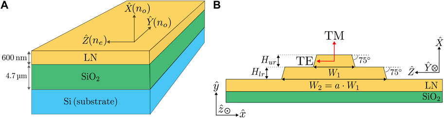
FIGURE 1. X-cut LNOI platform used for the waveguide design. (A) Schematic of the wafer where
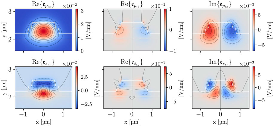
FIGURE 2. Components of the electric mode profile for the pump (upper row) and the signal (lower row), which showcase perfect PhM with the same (quasi-TE) polarization. The pump mode and the signal mode have equal effective index n ≈ 1.896.
3 Coupled-amplitude equations
The complex wavenumber is expressed as:
where nν is the effective refractive index of the relevant mode at the angular frequency ων, and c is the speed of light in vacuum. The case of continuous-wave (cw) excitation is considered, for which the complex electric and magnetic fields are decomposed as:
The complex vectors
The complex functions
The power is found from:
The complex wavenumber mismatch is defined as:
with Δβ = βs − 2βp and Δα = αs − 2αp. To ensure maximal coupling, perfect PhM should be achieved:
that is, the effective index of the pump must equal that of the signal. To maximize the signal power, a large modal overlap is preferred between the pump and the signal. The modal overlap is encompassed in the coupling coefficient:
with the second-order nonlinear susceptibility tensor D and a vector
Notice that the components of
4 Signal power and conversion efficiency
The pump power and signal power are computed from (3.5) by numerically solving the coupled-amplitude (Eqs 3.4a,3.4b), for
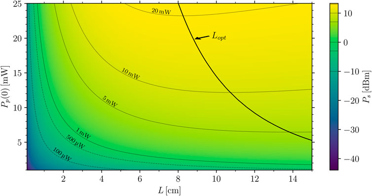
FIGURE 3. Signal power as a function of interaction length and on-chip pump power for the modes in Figure 2. Contours are plotted along with the Lopt curve, which marks the optimal interaction length that maximizes the signal power for a given on-chip pump power. Simulation data used for this plot have been linearly interpolated.
A key metric of interest is the conversion efficiency, which is a measure of the amount of the on-chip pump power, Pp(0), that is converted to signal power, Ps(L) after a given interaction length. As evident from Figure 3, the conversion efficiency is increasing with Pp(0) and the interaction length up until Lopt, where the conversion efficiency peaks at 86.4% for Pp(0) = 50 mW and L = 8.0 cm. In the undepleted pump approximation the conversion efficiency is proportional to on-chip pump power (Stanton et al., 2020), and it is therefore common practice in the literature (Hao et al., 2020); Rao et al. (2019); (Chen et al., 2018); to define the conversion efficiency per unit pump power:
or even further normalizing by the interaction length squared to compensate for the η ∝ L2 relation. These normalized conversion efficiency definitions are convenient metrics, since they allow one to compare conversion efficiencies for different materials and waveguide designs independently of the waveguide length and on-chip pump power. However, it is important to note that these definitions are based on the undepleted pump approximation, which is only reasonable for short waveguide and low on-chip pump powers. To provide feasible example where the definition in (Eq. 4.1) is appropriate, a 1 cm waveguide with Pp(0) = 10 mW is considered. From Figure 3; (Eq. 4.1) this yields a conversion efficiency of η = 3.92 W−1. The corresponding power spectrum of the signal is displayed in Figure 4 with a full-width-half-maximum (FWHM) of 0.17 nm.
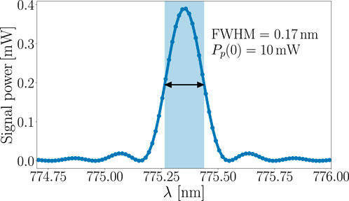
FIGURE 4. Signal power simulated as a function of the wavelength using an initial on-chip pump power of 10 mW. A FWHM of 0.17 nm is observed, as indicated by the arrow.
4.1 Fabrication tolerances
Deviations from the ideal waveguide geometry are in practice inevitable due to the various uncertainties associated with each intermediate step of waveguide fabrication. To address this, the margins of errors in fabrication are considered, and the impact that these have on the waveguide performance. To determine how robust the proposed design is, two parameters that are considered the most likely fabrication aberrations are investigated (see Figure 5A). Hence, this is not an extensive review of the fabrication tolerances of the design. Other aspects could be variations in the sidewall angle or the total thickness of the LN film and the impact that these have on the conversion efficiency (Chen et al., 2023).
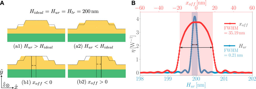
FIGURE 5. Fabrication tolerances of the conversion efficiency. (A) schematic of the fabrication aberrations from ideal waveguide structure. The contour of the ideal waveguide structure is marked with the dotted line for reference. (B) Conversion efficiency at an L = 1 cm interaction length as function of the offsets, xoff, and upper ridge heights, Hur. The simulation data used for this plot have been linearly interpolated.
The first aberration is the upper ridge height, Hur, which depends on how well the etching procedure is calibrated. If the etching rate is higher than expected, the upper ridge height will exceed the target height, i.e. Hur < Hideal = 200 nm (a1), while a lower etching rate will yield Hur < Hideal (a2). The second etching step is less critical since the etching time can be adjusted based on the etching rate from the first etching step. The other aberration is misaligned of the upper ridge relative to the lower ridge, defined as the horizontal distance, xoff, relative to the center of the lower ridge (b1 and b2). While alignment marks are typically placed on the chip to ensure the best possible alignment, misalignment is still a risk that needs to be addressed. Figure 5B displays the impact that the two aberrations have on the conversion efficiency. Here, it is evident that upper ridge height is by far the most critical parameter with a FWHM of 0.21 nm, while the conversion efficiency is more tolerant to misalignment with a FWHM of 35.19 nm. To ensure that a decent amount of signal power can still be generated for Hur ≠ Hideal, the remaining degrees of freedom for the waveguide geometry parameters are explored. This is done in Figure 6, where the upper ridge width, W1, is varied to compensate for the non-ideal upper ridge height to obtain PhM and thereby non-vanishing conversion efficiencies.
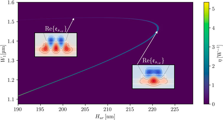
FIGURE 6. Conversion efficiency for the parameter space spanned by Hur and W1 evaluated at a interaction length of L = 1 cm and scaling parameter a = 1.3. In addition to the signal mode in Figure 2 associated with the upward-sloped segment, another higher-order mode displays perfect PhM (top flat segment), though with a lower conversion efficiency. The simulation data used for this plot have been linearly interpolated.
Here, there is a clear trend, where the conversion efficiency is non-vanishing. The ascending slope segment is associated with the higher-order signal mode in Figure 2, while the upper flat segment is related to another higher-order TE signal mode. The TE components of the two higher-order signal mode profiles are displayed along with the conversion efficiency trend. The mode profile at Hur ≈ 222 nm shows where the signal mode in Figure 2 transitions towards the other signal mode at Hur ≈ 203 nm. While the signal mode at Hur ≈ 203 nm has a lower coupling coefficient, κ = 1.34 ⋅ 10–5, and conversion efficiency, it is more tolerant to variations in Hur. By implementing a number of waveguides on a chip with varying W1 in the range 1.1–1.5 μm, one has chip design that is tolerant over a range of ±15 nm from the ideal etching depth.
5 Discussion
The conversion efficiency of 3.92 W−1 at L = 1 cm is about an order of magnitude lower than the state-of-the-art for single-pass SHG in GaAs-on-insulator Stanton et al. (2020). However, GaAs has high absorption at 775 nm (Casey et al., 1974), making it an unsuitable choice of material for this particular frequency conversion process. In comparison simulations of similar single-pass LN waveguides show η = 0.6 W−1 Wang et al. (2017) and η = 0.22 W−1 (Luo et al., 2018) at L = 1 cm, where the presented design has a notably higher conversion efficiency. Substantially higher conversion efficiencies can be achieved in ring resonators (Lu et al., 2019; Boes et al., 2021); however, this comes a the cost of a very narrow acceptance band-with for the phase matching condition. To increase the output power of single-pass design, such as to provide an output power that is viable for practical applications, multiple arrays of the same waveguides could be combined into a single laser source (Madsen et al., 2023). However, considering the narrower linewidth of the signal that can be generated from a resonating structure, a ring resonator implementation of the design has prospects for producing spectrally pure photons and, thereby, highly entangled photons.
The double ridge design was developed as a solution to the design restriction of a maximal 200 nm etching depth. However, recent advances in fabrication have enabled deeper etching, which opens up new waveguide design possibilities. While the higher-order mode associated with the upper flat trend in Figure 6 has a lower conversion efficiency compared to the signal mode in Figure 2, it is more tolerant to variations in Hur. This implies a trade-off between high conversion efficiency and a robust design. Regarding the implementation of the waveguide design on a chip and coupling light into the chip, there is an inherently good overlap between the fundamental TE waveguide mode, Figure 2 (upper row), and a Gaussian pump mode from the fiber, making edge coupling the apparent choice. However, considering the case of SPDC, the fiber mode must couple to the non-Gaussian higher order mode in Figure 2 (lower row). Here, difficulties arise since it is challenging to only couple to a single specific higher-order mode without also exciting other modes (Dave and Lipson, 2019).
6 Conclusion and outlook
Using the lithium niobate on insulator platform (Figure 1A), a double-ridge waveguide (Figure 1B) has been designed for second-harmonic generation at 775 nm from the infrared-C wavelength. Perfect phase matching is achieved between the fundamental TE waveguide mode at 1,550 nm and a higher-order TE mode at the second harmonic (Figure 2). This allows access to the largest element of the second-order nonlinear susceptibility tensor. From simulations, the generated second harmonic has a spectral full-width-half-maximum (FWHM) of 0.17 nm (Figure 4) for an initial on-chip pump power of 10 mW. This makes the design tolerant, and relevant in implementations such as cascaded SPDC (Zhang et al., 2021). Maximal conversion efficiencies is obtained for waveguides longer than 8 cm, which is beyond what is practicable for integrated circuits fabrication and applications. Considering a more viable waveguide length of 1 cm, a conversion efficiency of 3.92 W−1 is obtained, which is larger than reported from similar simulation studies of straight single-pass waveguides Wang et al. (2017); (Luo et al., 2018). Fabrication tolerances of the proposed waveguide design have been thoroughly investigated. In particular, deviations from the target thickness of the upper ridge have the most critical impact on the conversion efficiency. To compensate for non-ideal etching, the width of the upper ridge could be varied to achieve perfect phase matching and thereby nonvanishing conversion efficiencies. Here, an additional higher-order TE signal mode was found that is robust to variations in upper ridge thickness, though with a lower conversion efficiency. This allows one to find an optimum trade-off between a high-performing and robust design.
The natural next step is to fabricate and characterize the waveguide performance to validate the numerical results in Figures 3, 4. Initially, it should be characterized classically for SHG before advancing to the more complex experimental setup associated with detecting single photons generated from SPDC. In terms of coupling to the higher-order mode for the SPDC application, it makes great sense to optimize a grating coupler design that modulates the pump light such that the modal overlap between the pump and higher-order TE mode is maximized while reducing the amount of power from the pump that couples to the lower-order modes. In addition, there is a potential in using a pulsed laser source, instead of cw considered in this report, to increase the pump power and, thereby, the conversion efficiency. Now, there is a long list of requirements for single photon emitters, hereunder high indistinguishability, temporal purity, brightness, and repetition rates Aharonovich et al. (2016). Before the design qualifies to be a candidate for a single photon source, further work needs to be carried out to investigate the waveguide performance on these parameters in a quantum mechanical theoretical framework. However, as a starting point, the simulation results obtained from the waveguide design indicate an efficient frequency converter with high fabrication tolerances. Moreover, the waveguide design does not require poling, which, in turn, reduces the fabrication complexity. The design can hence be fabricated with mature technologies, which paves the way for a scalable SPDC source in the infrared-C band.
Data availability statement
The raw data supporting the conclusions of this article will be made available by the authors, without undue reservation.
Author contributions
MH: Writing–original draft. FL: Writing–review and editing. MM: Writing–review and editing. YD: Writing–review and editing. KR: Writing–review and editing. NV: Writing–review and editing.
Funding
The author(s) declare financial support was received for the research, authorship, and/or publication of this article. We acknowledge financial support from Innovation Fund Denmark (Innoexplorer, QVersion project), Villum Fonden (Young Investigator, QUANPIC project, ref. 00025298), and the Independent Research Fund Denmark (DFF, ref. 1032-00460B).
Conflict of interest
The authors declare that the research was conducted in the absence of any commercial or financial relationships that could be construed as a potential conflict of interest.
Publisher’s note
All claims expressed in this article are solely those of the authors and do not necessarily represent those of their affiliated organizations, or those of the publisher, the editors and the reviewers. Any product that may be evaluated in this article, or claim that may be made by its manufacturer, is not guaranteed or endorsed by the publisher.
References
Adcock, J. C., and Ding, Y. (2022). Quantum prospects for hybrid thin-film lithium niobate on silicon photonics. Front. Optoelectron. 15, 7. doi:10.1007/s12200-022-00006-7
Aharonovich, I., Englund, D., and Toth, M. (2016). Solid-state single-photon emitters. Nat. Photonics 10, 631–641. doi:10.1038/nphoton.2016.186
Basset, F. B., Valeri, M., Neuwirth, J., Polino, E., Rota, M. B., Poderini, D., et al. (2023). Daylight entanglement-based quantum key distribution with a quantum dot source. Quantum Sci. Technol. 8, 025002. doi:10.1088/2058-9565/acae3d
Boes, A., Chang, L., Nguyen, T., Ren, G., Bowers, J., and Mitchell, A. (2021). Efficient second harmonic generation in lithium niobate on insulator waveguides and its pitfalls. J. Phys. Photonics 3, 012008. doi:10.1088/2515-7647/abd23a
Briggs, I., Hou, S., Cui, C., and Fan, L. (2021). Simultaneous type-I and type-II phase matching for second-order nonlinearity in integrated lithium niobate waveguide. Opt. Express 29, 26183. doi:10.1364/OE.430438
Casey, H. C., Sell, D. D., and Wecht, K. W. (1974). Concentration dependence of the absorption coefficient for n and ptype GaAs between 1.3 and 1.6 eV. J. Appl. Phys. 46, 250–257. doi:10.1063/1.321330
Chang, L., Li, Y., Volet, N., Wang, L., Peters, J., and Bowers, J. E. (2016). Thin film wavelength converters for photonic integrated circuits. Optica 3, 531. doi:10.1364/OPTICA.3.000531
Chen, P.-K., Briggs, I., Cui, C., Zhang, L., Shah, M., and Fan, L. (2023). Adapted poling to break the nonlinear efficiency limit in nanophotonic lithium niobate waveguides. Nat. Nanotechnol., 1–7. doi:10.1038/s41565-023-01525-w
Chen, P.-K., Briggs, I., Hou, S., and Fan, L. (2022). Ultra-broadband quadrature squeezing with thin-film lithium niobate nanophotonics. Opt. Lett. 47, 1506–1509. doi:10.1364/OL.447695
Chen, Y., Zopf, M., Keil, R., Ding, F., and Schmidt, O. G. (2018). Highly-efficient extraction of entangled photons from quantum dots using a broadband optical antenna. Nat. Commun. 9, 2994–2997. doi:10.1038/s41467-018-05456-2
Dave, U. D., and Lipson, M. (2019). “Efficient conversion to very high order modes in silicon waveguides,” in Conference on Lasers and Electro-Optics, San Jose, CA, USA, May, 2019. doi:10.1364/CLEO_SI.2019.SM3J.6
Guo, X., Zou, C.-l., Schuck, C., Jung, H., Cheng, R., and Tang, H. X. (2017). Parametric down-conversion photon-pair source on a nanophotonic chip. Light Sci. Appl. 6, e16249. doi:10.1038/lsa.2016.249
Hao, Z., Zhang, L., Mao, W., Gao, A., Gao, X., Gao, F., et al. (2020). Second-harmonic generation using d 33 in periodically poled lithium niobate microdisk resonators. Photonics Res. 8, 311. doi:10.1364/PRJ.382535
Helt, L. G., Liscidini, M., and Sipe, J. E. (2012). How does it scale? Comparing quantum and classical nonlinear optical processes in integrated devices. J. Opt. Soc. Am. B 29, 2199. doi:10.1364/JOSAB.29.002199
Holewa, P., Ostój-Ziȩba, E., Vajner, D. A., Gao, T., Lach, M., Wasiluk, M., et al. (2023). “State-of-the-art quantum dot-based single-photon sources for quantum key distribution in silica fiber networks at 1550 nm,” in 51st International School & Conference on the Physics of Semiconductors, Szczyrk, Poland, June, 2023.
Huber, D., Reindl, M., Huo, Y., Huang, H., Wildmann, J. S., Schmidt, O. G., et al. (2017). Highly indistinguishable and strongly entangled photons from symmetric GaAs quantum dots. Nat. Commun. 8, 15506. doi:10.1038/ncomms15506
Hunsperger, R. G. (2002). “Integrated optics: theory and technology,” in Advanced texts in physics (Berlin, Germany: Springer). doi:10.1007/978-3-540-38843-2
Kozlov, A., Moskalev, D., Salgaeva, U., Bulatova, A., Krishtop, V., Volyntsev, A., et al. (2023). Reactive ion etching of X-cut LiNbO3 in an ICP/TCP system for the fabrication of an optical ridge waveguide. Appl. Sci. 13, 2097. doi:10.3390/app13042097
Krasnokutska, I., Tambasco, J.-L. J., Li, X., and Peruzzo, A. (2018). Ultra-low loss photonic circuits in lithium niobate on insulator. Opt. Express 26, 897–904. doi:10.1364/OE.26.000897
Lodahl, P., Ludwig, A., and Warburton, R. J. (2022). A deterministic source of single photons. Phys. Today 75, 44–50. doi:10.1063/PT.3.4962
Lu, J., Surya, J. B., Liu, X., Bruch, A. W., Gong, Z., Xu, Y., et al. (2019). Periodically poled thin film lithium niobate microring resonators with a second-harmonic generation efficiency of 250,000%/W. Optica 6, 1455. doi:10.1364/OPTICA.6.001455
Luo, R., He, Y., Liang, H., Li, M., and Lin, Q. (2018). Highly tunable efficient second-harmonic generation in a lithium niobate nanophotonic waveguide. Optica 5, 1006–1011. doi:10.1364/OPTICA.5.001006
Madsen, M. L., Ulsig, E. Z., Folsach, S., Godoy, P. H., Stanton, E. J., and Volet, N. (2023). Mid-infrared difference-frequency generation in AlGaAs-on-insulator waveguides. JOSA B 40, 1742–1748. doi:10.1364/JOSAB.488065
Malitson, I. H. (1965). Interspecimen comparison of the refractive index of fused silica. JOSA 55, 1205–1209. doi:10.1364/JOSA.55.001205
Niu, Y., Yan, X., Chen, J., Ma, Y., Zhou, Y., Chen, H., et al. (2022). Research progress on periodically poled lithium niobate for nonlinear frequency conversion. Infrared Phys. Technol. 125, 104243. doi:10.1016/j.infrared.2022.104243
O’Brien, J. L., Furusawa, A., and Vučković, J. (2009). Photonic quantum technologies. Nat. Photonics 3, 687–695. doi:10.1038/nphoton.2009.229
Pu, M., Zheng, Y., Stassen, E., Kamel, A. N., Bony, P.-Y., Ottaviano, L., et al. (2018). “Nano-engineered high-confinement AlGaAs waveguide devices for nonlinear photonics,” in Nanophotonics. Editors D. L. Andrews, J.-M. Nunzi, A. Ostendorf, and A. J. Bain (Strasbourg, France: SPIE). doi:10.1117/12.2307114
Rao, A., Abdelsalam, K., Sjaardema, T., Honardoost, A., Camacho-Gonzalez, G. F., and Fathpour, S. (2019). Actively-monitored periodic-poling in thin-film lithium niobate photonic waveguides with ultrahigh nonlinear conversion efficiency of 4600 %W−1cm−2. Opt. Express 27, 25920–25930. doi:10.1364/OE.27.025920
Shah, M., Briggs, I., Chen, P.-K., Hou, S., and Fan, L. (2023). Visible-telecom tunable dual-band optical isolator based on dynamic modulation in thin-film lithium niobate. Opt. Lett. 48, 1978–1981. doi:10.1364/OL.482635
Shams-Ansari, A., Huang, G., He, L., Li, Z., Holzgrafe, J., Jankowski, M., et al. (2022). Reduced material loss in thin-film lithium niobate waveguides. Apl. Photonics 7, 081301. doi:10.1063/5.0095146
Stanton, E. J., Chiles, J., Nader, N., Moody, G., Volet, N., Chang, L., et al. (2020). Efficient second harmonic generation in nanophotonic GaAs-on-insulator waveguides. Opt. Express 28, 9521. doi:10.1364/OE.389423
Uppu, R., Midolo, L., Zhou, X., Carolan, J., and Lodahl, P. (2021). Quantum-dot-based deterministic photon–emitter interfaces for scalable photonic quantum technology. Nat. Nanotechnol. 16, 1308–1317. doi:10.1038/s41565-021-00965-6
Wang, C., Xiong, X., Andrade, N., Venkataraman, V., Ren, X.-F., Guo, G.-C., et al. (2017). Second harmonic generation in nano-structured thin-film lithium niobate waveguides. Opt. Express 25, 6963–6973. doi:10.1364/OE.25.006963
Wang, Y., Faurby, C. F. D., Ruf, F., Sund, P. I., Nielsen, K., Volet, N., et al. (2023). Deterministic photon source interfaced with a programmable silicon-nitride integrated circuit. npj Quantum Inf. 9, 94–95. doi:10.1038/s41534-023-00761-1
Wolf, R., Breunig, I., Zappe, H., and Buse, K. (2018). Scattering-loss reduction of ridge waveguides by sidewall polishing. Opt. Express 26, 19815–19820. doi:10.1364/OE.26.019815
Zelmon, D. E., Small, D. L., and Jundt, D. (1997). Infrared corrected Sellmeier coefficients for congruently grown lithium niobate and 5 mol. % magnesium oxide–doped lithium niobate. JOSA B 14, 3319–3322. doi:10.1364/JOSAB.14.003319
Zhang, M., Wang, C., Cheng, R., Shams-Ansari, A., and Lončar, M. (2017). Monolithic ultra-high-Q lithium niobate microring resonator. Optica 4, 1536–1537. doi:10.1364/OPTICA.4.001536
Zhang, W., van Leent, T., Redeker, K., Garthoff, R., Schwonnek, R., Fertig, F., et al. (2022). A device-independent quantum key distribution system for distant users. Nature 607, 687–691. doi:10.1038/s41586-022-04891-y
Zhang, Z., Yuan, C., Shen, S., Yu, H., Zhang, R., Wang, H., et al. (2021). High-performance quantum entanglement generation via cascaded second-order nonlinear processes. npj Quantum Inf. 7, 123–129. doi:10.1038/s41534-021-00462-7
Keywords: thin-film LNOI, frequency conversion, second-harmonic generation, single photons, higher-order modes, nonlinear waveguides
Citation: Hansen MT, Ulsig EZ, Labbé F, Madsen ML, Ding Y, Rottwitt K and Volet N (2023) Efficient and robust second-harmonic generation in thin-film lithium niobate using modal phase matching. Front. Photonics 4:1324648. doi: 10.3389/fphot.2023.1324648
Received: 19 October 2023; Accepted: 20 November 2023;
Published: 06 December 2023.
Edited by:
Yu Zhang, HyperLight Corp, United StatesCopyright © 2023 Hansen, Ulsig, Labbé, Madsen, Ding, Rottwitt and Volet. This is an open-access article distributed under the terms of the Creative Commons Attribution License (CC BY). The use, distribution or reproduction in other forums is permitted, provided the original author(s) and the copyright owner(s) are credited and that the original publication in this journal is cited, in accordance with accepted academic practice. No use, distribution or reproduction is permitted which does not comply with these terms.
*Correspondence: Mikkel T. Hansen, dG9ycmlsZEBlY2UuYXUuZGs=