All-Inorganic Perovskite CsPb2Br5 Microsheets for Photodetector Application
 Xiaosheng Tang1*
  Shuai Han1
  Zhiqiang Zu1 Wei Hu1 Dan Zhou2* Juan Du3 Zhiping Hu1 Shiqi Li1 Zhigang Zang1
- 1Key Laboratory of Optoelectronic Technology and Systems of the Education Ministry of China, College of Optoelectronic Engineering, Chongqing University, Chongqing, China
- 2Chongqing Key Laboratory of Extraordinary Bond Engineering and Advanced Materials Technology, College of Mechanical and Electrical Engineering, Yangtze Normal University, Chongqing, China
- 3State Key Laboratory of High Field Laser Physics, Shanghai Institute of Optics and Fine Mechanics, Chinese Academy of Sciences, Shanghai, China
Lead-halide perovskites have emerged as one kind of important optoelectronic materials with excellent performance in photovoltaic and light-emitting diode applications. Herein, we reported all-inorganic perovskite CsPb2Br5 microsheets prepared by a facile injection method. Through the X-ray diffraction (XRD) and Scanning Electron Microscope (SEM), it could be seen that the CsPb2Br5 microsheets showed single tetragonal crystalline phase and kept uniform square shape. Moreover, the as-synthesized CsPb2Br5 microsheets exhibited photoluminescence emission at 513 nm, and the UV–vis absorption spectrum further indicated the band gap of CsPb2Br5 microsheets was ≈2.50 eV. Additionally, the as-fabricated CsPb2Br5 microsheets based photodetector exhibited faster photoresponse characteristics of short rise time (0.71 s) and decay time (0.60 s), which demonstrated its promising application as high performance electronic and optoelectronic devices.
Introduction
Two dimensional (2D) nanostructures, such as BN [1], MoS2 [2], and WS2 [3] have attracted increasing attention due to the unique properties and are widely studied in many fields ranging from energy storage to environmental protection [4, 5]. Compared with one dimensional (1D) and zero dimensional (0D) nanostructures, 2D nanostructures materials show great advantages in some special applications attributed to their extraordinary electrical, optical and magnetic properties [6–8]. Recently, various kinds of semiconductor nanostructure materials are employed in photodetectors application as the reason of their high absorption coefficient, tunable bandgap, and high quantum yield [9, 10]. In the last 2 years, the halide perovskite materials were demonstrated to be amazing semiconductors with high performance. As a new family of photoelectric materials, metal halide perovskite nanocrystals have received a revival of interest based on its outstanding optoelectronic characteristics including tunable band-gap property [11], high power conversion efficiency [9], broad absorption spectrum [12], high charge carrier mobility [13], and long charge diffusion lengths [14]. However, there are few reports about the optoelectronic application based on 2D perovskite microstructure.
As one kind of the perovskites nanomaterials, all-inorganic lead halide perovskites CsPbX3 (X = I, Br, Cl) are generally recognized as one probable substitute of organic perovskites [15, 16]. To date, all-inorganic cesium lead halide perovskite have generated considerable attention because of their higher stability and outstanding optoelectronic properties comparable to the hybrid organic–inorganic perovskites [17–20]. Thus, a large number of CsPbX3 (X = I, Br, Cl) perovskite nanostructures such as nanocrystals [21], nanowires [22], microsheets [23, 24], nanocubes, were prepared by solution processing approach. Furthermore, the physical properties of all-inorganic nanocrystals could be adjusted by their geometric shape and size [25]. For example, Deng et al. prepared CsPbBr3 nanocrystals with various shapes including nanocubes, nanorods, and nanoplatelets, by choosing different ligands during reprecipitation process at room temperature [26]. Therefore, more and more researchers begun to pay attention to the CsPbX3 (X = I, Br, Cl) based photodetectors including nano-films, nanoparticles, and nonarods. More recently, CsPb2Br5 as a new perovskite crystal structure has emerged as attractive semiconducting material. Wang et al. reported a new type of highly luminescent perovskite-related CsPb2Br5 nanoplatelets via a facile precipitation reaction [27]. Jiang's group synthesized tetragonal CsPb2Br5 nanosheets which was an indirect bandgap semiconductor [28]. However, there are few corresponding applications which have been further referred up to now for this kind of excellent materials. Therefore, it is interesting and necessary to carry on the study of optoelectronic application based on CsPb2Br5 microsheets.
In this work, we demonstrated an efficient approach for synthesis of perovskite-related uniform CsPb2Br5 microsheets with the size of 4.2 × 4.2 μm. The detailed structural characterization revealed that these microsheets were single-crystalline with uniform growth direction, and crystallized in pure tetragonal phase. The optical and electrical properties of the as-prepared microsheets were investigated in detail. The as-prepared CsPb2Br5 microsheets exhibited compositional bandgap engineering through the entire visible spectral region of 380–525 nm. PL peak appeared at 513 nm with a narrow emission line widths of 23 nm. In particular, photodetector devices based on entirely all-inorganic CsPb2Br5 microsheets were demonstrated for the first time. The photodetectors exhibited relatively fast rise and decay times of 0.71 and 0.60 s, respectively.
Experimental
The generalized protocol for synthesizing CsPb2Br5 perovskite microsheets was developed by modifying solution-based precipitation process initially adopted by Yang et al. [22]. Briefly, Cs2CO3 (100 mg), oleic acid (0.4 ml, OA), and octadecene (3.75 ml, ODE) were loaded in a 100 ml three-neck flask and heated under nitrogen flow at 120°C for 1 h to obtain Cs-oleate precursor. Then, PbBr2 (0.36 mmol) was dissolved in ODE (5 ml) in a new 100 ml three neck flask at 120°C having nitrogen flow. After 1 h, oleylamine (0.5 ml, OLA) and OA (0.8 ml) were added to the mixture and heated to 135°C to keep 0.5 h, followed by swift injection of the Cs-oleate precursor (0.5 mL). The reaction was maintained with the environment of nitrogen at 135°C for 1.5 h, then, was cooled by the ice bath. The CsPb2Br5 product were centrifuged, precipitated, and dispersed in toluene for characterization. The schematic of synthesis for CsPb2Br5 microsheets was illustrated in Figure 1.
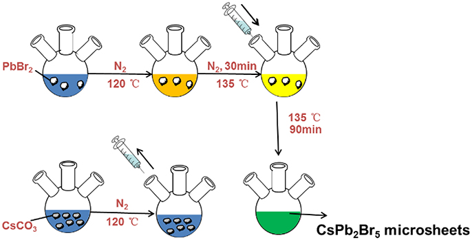
Figure 1. The schematic of the synthesis for CsPb2Br5 microsheets.
The crystal phases of all samples were characterized by X-ray diffraction (XRD) with Cu Kα radiation (XRD-6100, SHIMADZU, Japan). The surface morphology and composition were observed by scanning electron microscopy (SEM, JSM-7800F) with X-ray energy dispersive spectrometry (XEDS). Atomic force microscopy (AFM) imaging was carried out on a scanning probe microscope (Nanonavi, SPA-400SPM, Japan) using a tapping mode. The absorption spectra was adopted by a Scan UV-vis spectrophotometer (UV-vis: UV-2100, Shimadzu, Japan), while photoluminescence (PL) spectra were measured by a fluorescence spectrophotometer (PL: Agilent Cary Eclipse, Australia) which included a Xe lamp as an excitation source with optical filters). The transmission electron microscopy (TEM) and high-resolution TEM (HRTEM) images were obtained using a ZEISS LIBRA 200FE microscope. The on/off photocurrent ratio of the CsPb2Br5 microsheets was obtained by a source meter (Keithley 4200).
Results and Discussion
To get clear information about the CsPb2Br5 microsheets, the powder X-ray diffraction (XRD) was used to characterize the crystallographic structure of the as-obtained CsPb2Br5 microsheets. Figure 2 shows XRD pattern of the CsPb2Br5 microsheets, all of the characteristic diffraction peaks could be indexed into a tetragonal phase (PDF#25-0211), which was in good agreement with literature data for the tetragonal perovskite structure [27]. The crystal planes were marked on the XRD pattern. The diffraction peaks were strong and sharp, which indicated that the obtained CsPb2Br5 microsheets were highly crystalline. Moreover, there were no any impurity peaks detected in the sample, suggesting its high crystalline quality of the as-prepared CsPb2Br5 microsheets.
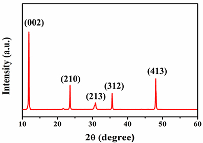
Figure 2. XRD pattern of CsPb2Br5 microsheets.
Additionally, in order to study the morphology of CsPb2Br5 microsheets, Scanning Electron Microscope (SEM) was employed for observation. From Figure 3a, it could be seen that the as-synthesized CsPb2Br5 microstructures were square shape with average lateral size (4.2 × 4.2 μm), and there were few by-products, which suggested the high purity of CsPb2Br5 microsheets. X-ray energy dispersive spectrometry (XEDS) measurement was performed to identify the composition of the as-obtained microsheets, as shown in Figure 3b. It could be seen that the composition elements were determined as Cs, Pb, and Br elements, and the Cs/Pb/Br atomic ratio was determined as 11.7/22.5/65.8. To investigate the distribution states, XEDS elemental mappings were carried out on the surface of CsPb2Br5 microsheet. Figure 3c shows the single typically CsPb2Br5 microsheet, and accordingly elemental XEDS mappings (Figures 3d–f) were measured in this area. The XEDS elemental mapping images further indicated the homogeneous distribution of Br (Figure 3d), Cs (Figure 3e) and Pb (Figure 3f) elements within individual microsheet. The thickness of as-synthesized CsPb2Br5 microsheets was measured by atomic force microscope (AFM). The AFM image (Figure 3g) and line profile (Figure 3h) showed that the thickness of the CsPb2Br5 microsheets was about 21 nm.
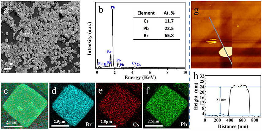
Figure 3. (a) SEM images of CsPb2Br5 microsheets; (b) XEDS analysis of the CsPb2Br5 microsheets; (c) SEM image of an individual CsPb2Br5 microsheet; (d–f) XEDS elemental images of the CsPb2Br5 microsheets (blue, Br; red, Cs; green, Pb) for a single CsPb2Br5 microsheet; (g–h) AFM image and the thickness measurement of CsPb2Br5 microsheets.
The morphology of the CsPb2Br5 thin microsheet (4.2 × 4.2 μm) was further tested by typical TEM, as showed in Figure 4a. Figure 4b was the high-resolution transmission electron microscopy (HRTEM) image of single CsPb2Br5 microsheet, it could be obviously observed that the interplanar distances was about 0.37 nm, which could be assigned as the lattice (202) planes of the tetragonal structure. And the clear lattice also confirmed the CsPb2Br5 microsheets had high quality crystalline, which matched well with the XRD results.
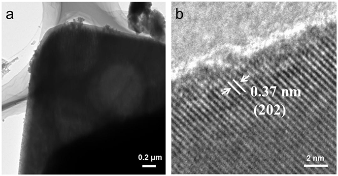
Figure 4. (a) TEM and (b) HRTEM images of CsPb2Br5 microsheet.
As the excellent properties of the as-prepared CsPb2Br5 microsheets, it has been studied as lasing application in our previous work [29]. Herein, the large lateral dimensions of these perovskite microsheets motivated us to explore their potential applications in optoelectronic devices. As shown in Figure 5a, a simple photodetector device was fabricated by dropping the CsPb2Br5 microsheets onto gold interdigital electrode with 3 μm spacing between adjacent fingers. The light source used in this device was a continuous wave laser (excitation at 405 nm with an optical power of 20 mW), otherwise, the bias voltage could be adjusted from 1 to 30 V for testing the photoresponse activity. In order to clearly illustrate the structure of the device, a typical SEM image of the CsPb2Br5 microsheets based photodetector is showed in Figure 5b. It could be observed that some of the as-prepared CsPb2Br5 microsheets were successfully crossed on two gold electrodes, which demonstrated the good devices.
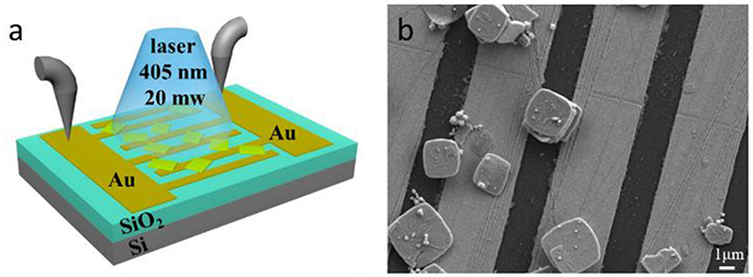
Figure 5. (a) Schematic of a photodetector device based on CsPb2Br5 microsheets. (b) The SEM image of real photodetector device.
The optical properties of the CsPb2Br5 microsheets films were characterized by UV–vis absorption and photoluminescence (PL) spectra, as showed in Figure 6A. The CsPb2Br5 microsheets had an absorption spectrum that was dominated by sharp exciton peaks, as similar to the optical features of previously reports [24, 27]. Furthermore, the absorption intensity was lower than the orthorhombic CsPbBr3, further suggesting that the CsPb2Br5 microsheets were successfully obtained [28]. The absorption spectrum (blue line) exhibited an absorption peak at around 495 nm, yielding an excitonic bandgap of about 2.50 eV [30, 31]. The PL emission spectrum (red line) exhibited a highly symmetric form located at 513 nm (≈2.42 eV) with a narrow full width at half maximum (FWHM) of 23 nm. No sub-bandgap emission was observed in the PL spectrum, indicating that CsPb2Br5 microsheets can be employed in photodetectors [32]. PL properties of the CsPb2Br5 were convinced by our group, and the CsPb2Br5 can remain stable under ambient environment [29, 33].
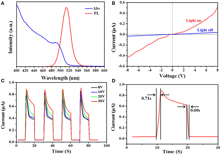
Figure 6. (A) Spectrum of fluorescence (excited by light with λ = 365 nm) (red line) and absorption (blue line) for CsPb2Br5 microsheets. (B) I–V curves of the photodetector measured in the dark and under illumination using a 405 nm laser diode by sweeping the voltage from −8 to 8 V. (C) Photocurrent-time response of the photodetector measured in the dark and with 405 nm illuminating with a bias of 8, 10, 20, and 30 V. (D) The rise time and the decay time of the photo-detector device.
Current–voltage (I–V) characteristics of the CsPb2Br5 microsheets based photodetector under the dark and illumination with 405 nm light are illustrated in Figure 6B. The room temperature I–V curves were measured at different bias voltage ranging from −8 to 8 V in air. Clearly, I–V curves presented linear dependence on the applied bias, indicating a good ohmic contact between CsPb2Br5 microsheets and gold electrodes [34]. The photo-excited current increased by more than 13 times compared with the dark current, indicating the ultimately high sensitivity of the photodetector. The increase in current under illumination could be attributed to the large amounts of electron-hole pairs generated by the photon absorption and subsequently extracted by the electrical field [35].
Photoresponsivity is also one critical factor used to evaluate the performance of photodetectors. Figure 6C illustrates the photoresponse behavior of the photodetector based CsPb2Br5 microsheets, which was measured in the dark and with 405 nm illuminating periodically at a different bias of 8, 10, 20, and 30 V, respectively. It could be observed that upon illumination, the photocurrent rapidly increased drastically due to the increase in carrier drift velocity and then drastically decreased to its initial level when the light was turned off, indicating the higher stability and reproducible characteristics of the photodetector device [35]. Also, it could be seen that the photocurrent increased when the applied voltage was elevated. At a bias of 30 V, the dark current was 0.03 μA and when the flexible device was under illuminated, the photocurrent increased to 0.89 μA, showing a photocurrent on/off ratio of 30. It should be noted that the applied bias voltage influenced the on/off ratio of the devices, which was caused by the exciton dissociation and the background current [36].
The time response speed is usually recognized as one key factor for evaluating the performance of sensor and it could determine the capability of photodetector. Figure 6D shows the response time and recovery time of our device, which were found to be around 0.71 and 0.60 s, respectively. Both of them are shorter than 1 s, which are significantly faster compared with the previously reported perovskite detectors [37–39]. And, the faster response speed of this CsPb2Br5 thin microsheets based photodetector could be ascribed to the high crystal quality of as-prepared CsPb2Br5 microsheets, which guaranteeing the efficient optical absorption and photogeneration of carriers. On the other side, the short transit time and large surface-to-volume ratio of CsPb2Br5 thin microsheets tend to induce defects and dangling bonds on the surface of microsheets [40, 41]. The switching in the two states exhibited faster photoresponse characteristics, allowing the device to act as a high-quality photosensitive switch.
Conclusions
In summary, we have synthesized the CsPb2Br5 microsheets through a low-cost injection method. The characterization results of XRD, SEM, and HRTEM confirmed that the as-grown CsPb2Br5 microsheets were single crystalline and had uniform tetragonal morphology. The optical band gap of the CsPb2Br5 microsheets was found to be ≈2.50 eV and the PL emission peak was located at around 513 nm with a 23 nm FWHM. Besides, photodetector based on CsPb2Br5 microsheets was fabricated and studied for the first time, exhibiting great photoresponse with the response time (0.71 s) and decay time (0.60 s). All these unique characteristics suggested that CsPb2Br5 microsheet is a promising material for photodetection applications.
Author Contributions
XT did the major work of this manuscript including synthesis process, characterization, and writing; SH, ZZu, ZH, and SL synthesized part of perovskite CsPb2Br5 microsheets; WH, DZ, and ZZa gave some supports on the TEM and SEM testing; JD gave some suggestion and comments on writing paper.
Conflict of Interest Statement
The authors declare that the research was conducted in the absence of any commercial or financial relationships that could be construed as a potential conflict of interest.
Acknowledgments
This work is supported by National Natural Science Foundation of China (61520106012, 61674023), the Fundamental Research Funds for the Central Universities (106112015CDJZR125511, 106112015CDJXY120001, 106112016CDJCR121222), initial funding of Hundred Young Talents Plan at Chongqing University (0210001104430), The Chongqing Research Program of Basic Research and Frontier Technology (cstc2015jcyjA1055, cstc2015jcyjA90007), the Project-sponsored by SRF for ROCS, SEM (0210002409003).
References
1. Yao YG, Lin ZY, Li Z, Song XJ, Moon KS, Wong CP. Large-scale production of two-dimensional nanosheets. J Mater Chem. (2012) 22:13494–99. doi: 10.1039/c2jm30587a
2. Yin Z, Li H, Li H, Jiang L, Shi Y, Sun Y, et al. Single-layer MoS2 phototransistors. ACS Nano (2012) 6:74–80. doi: 10.1021/nn2024557
3. Tan H, Fan Y, Zhou Y, Chen Q, Xu W, Warner JH. Ultrathin 2D photodetectors utilizing chemical vapor deposition grown WS2 with graphene electrodes. ACS Nano (2016) 10:7866–73. doi: 10.1021/acsnano.6b03722
4. Jariwala D, Sangwan VK, Lauhon LJ, Marks TJ, Hersam MC. Emerging device applications for semiconducting two-dimensional transition metal dichalcogenides. ACS Nano (2014) 8:1102–20. doi: 10.1021/nn500064s
5. Coleman JN, Lotya M, O'Neill A, Bergin SD, King PJ, Khan U, et al. Two-dimensional nanosheets produced by liquid exfoliation of layered materials. Science (2011) 331:568–71. doi: 10.1126/science.1194975
6. Cho M. Coherent two-dimensional optical spectroscopy. Chem Rev. (2008) 108:1331–418. doi: 10.1021/cr078377b
7. Buscema M, Island JO, Groenendijk DJ, Blanter SI, Steele GA, van der Zant HS. Photocurrent generation with two-dimensional van der Waals semiconductors. Chem Soc Rev. (2015) 44:3691–718. doi: 10.1039/C5CS00106D
8. Dhanabalan SC, Ponraj JS, Zhang H, Bao Q. Present perspectives of broadband photodetectors based on nanobelts, nanoribbons, nanosheets and the emerging 2D materials. Nanoscale (2016) 8:6410–34. doi: 10.1039/C5NR09111J
9. Park NG. Organometal perovskite light absorbers toward a 20% efficiency low-cost solid-state mesoscopic solar cell. J Phys Chem Lett. (2013) 4:2423–9. doi: 10.1021/jz400892a
10. Wang X, Tian W, Liao M, Bando Y, Golberg D. Recent advances in solution-processed inorganic nanofilm photodetectors. Chem Soc Rev. (2014) 43:1400–22. doi: 10.1039/C3CS60348B
11. Eperon GE, Stranks SD, Menelaou C, Johnston MB, Herz LM, Snaith HJ. Formamidinium lead trihalide: a broadly tunable perovskite for efficient planar heterojunction solar cells. Energy Environ Sci. (2014) 7:982–8. doi: 10.1039/c3ee43822h
12. Kim HS, Lee CR, Im JH, Lee KB, Moehl T, Marchioro A, et al. Lead iodide perovskite sensitized all-solid-state submicron thin film mesoscopic solar cell with efficiency exceeding 9%. Sci Rep. (2012) 2:591. doi: 10.1038/srep00591
13. Wright AD, Verdi C, Milot RL, Eperon GE, Pérez-Osorio MA, Snaith HJ, et al. Electron-phonon coupling in hybrid lead halide perovskites. Nat Commun. (2016) 7:11755. doi: 10.1038/ncomms11755
14. Stranks SD, Eperon GE, Grancini G, Menelaou C, Alcocer MJ, Leijtens T, et al. Electron-hole diffusion lengths exceeding 1 micrometer in an organometal trihalide perovskite absorber. Science (2013) 342:341–4. doi: 10.1126/science.1243982
15. Tang X, Zu Z, Shao H, Hu W, Zhou M, Deng M, et al. All-inorganic perovskite CsPb(Br/I)3 nanorods for optoelectronic application. Nanoscale (2016) 8:15158–61. doi: 10.1039/C6NR01828A
16. Lv L, Xu Y, Fang H, Luo W, Xu F, Liu L, et al. Generalized colloidal synthesis of high-quality, two-dimensional cesium lead halide perovskite nanosheets and their applications in photodetectors. Nanoscale (2016) 8:13589–96. doi: 10.1039/C6NR03428D
17. Kulbak M, Cahen D, Hodes G. How important is the organic part of lead halide perovskite photovoltaic cells? Efficient CsPbBr3 cells. J Phys Chem Lett. (2015) 6:2452–6. doi: 10.1021/acs.jpclett.5b00968
18. Song J, Xu L, Li J, Xue J, Dong Y, Li X, et al. Monolayer and few-layer all-inorganic perovskites as a new family of two-dimensional semiconductors for printable optoelectronic devices. Adv Mater. (2016) 28:4861–9. doi: 10.1002/adma.201600225
19. Protesescu L, Yakunin S, Bodnarchuk MI, Krieg F, Caputo R, Hendon CH, et al. Nanocrystals of cesium lead halide perovskites (CsPbX3, X = Cl, Br, and I): novel optoelectronic materials showing bright emission with wide color gamut. Nano Lett. (2015) 15:3692–6. doi: 10.1021/nl5048779
20. Song J, Li J, Li X, Xu L, Dong Y, Zeng H. Quantum dot light-emitting diodes based on inorganic perovskite cesium lead halides (CsPbX3). Adv Mater. (2015) 27:7162–7. doi: 10.1002/adma.201502567
21. Lignos I, Stavrakis S, Nedelcu G, Protesescu L, deMello AJ, Kovalenko MV. Synthesis of cesium lead halide perovskite nanocrystals in a droplet-based microfluidic platform: fast parametric space mapping. Nano Lett. (2016) 16:1869–77. doi: 10.1021/acs.nanolett.5b04981
22. Zhang D, Eaton SW, Yu Y, Dou L, Yang P. Solution-phase synthesis of cesium lead halide perovskite nanowires. J Am Chem Soc. (2015) 137:9230–3. doi: 10.1021/jacs.5b05404
23. Akkerman QA, Motti SG, Srimath Kandada AR, Mosconi E, D'Innocenzo V, Bertoni G, et al. Solution synthesis approach to colloidal cesium lead halide perovskite nanoplatelets with monolayer-level thickness control. J Am Chem Soc. (2016) 138:1010–16. doi: 10.1021/jacs.5b12124
24. Bekenstein Y, Koscher, BA, Eaton SW, Yang P, Alivisatos AP. Highly luminescent colloidal nanoplates of perovskite cesium lead halide and their oriented assemblies. J Am Chem Soc. (2015) 137:16008–11. doi: 10.1021/jacs.5b11199
25. Grim JQ, Manna L, Moreels I. A sustainable future for photonic colloidal nanocrystals. Chem Soc Rev. (2015) 44:5897–914. doi: 10.1039/C5CS00285K
26. Sun S, Yuan D, Xu Y, Wang A, Deng Z. Ligand-mediated synthesis of shape-controlled cesium lead halide perovskite nanocrystals via reprecipitation process at room temperature. ACS Nano (2016) 10:3648–57. doi: 10.1021/acsnano.5b08193
27. Wang KH, Wu L, Li L, Yao HB, Qian HS, Yu SH. Large-scale synthesis of highly luminescent perovskite-related CsPb2Br5 nanoplatelets and their fast anion exchange. Angew Chem Int Ed. (2016) 55:8328–32. doi: 10.1002/anie.201602787
28. Li G, Wang H, Zhu Z, Chang Y, Zhang T, Song Z. Shape and phase evolution from CsPbBr3perovskite nanocubes to tetragonal CsPb2Br5nanosheets with an indirect bandgap. Chem Commun. (2016) 52:11296–9. doi: 10.1039/C6CC05877A
29. Tang X, Hu Z, Yuan W, Hu W, Shao H, Han D, et al. Perovskite CsPb2Br5 microplate laser with enhanced stability and tunable properties. Adv Opt Mater. (2017) 5:1600788. doi: 10.1002/adom.201600788
30. Green MA, Jiang Y, Soufiani AM, Ho-Baillie A. Optical properties of photovoltaic organic-inorganic lead halide perovskites. J Phys Chem Lett. (2015) 6:4774–85. doi: 10.1021/acs.jpclett.5b01865
31. Zhang Y, Fluegel B, Hanna MC, Geisz JF, Wang LW, Mascarenhas A. Effects of heavy nitrogen doping in III–V semiconductors– How well does the conventional wisdom holdfor the dilute nitrogen“III–V-N alloys”? Phys Stat Sol. (2003) 240:396–403. doi: 10.1002/pssb.200303329
32. Li Y, Shi ZF, Li S, Lei LZ, Ji HF, Wu D, et al. High-performance perovskite photodetectors based on solution-processed all-inorganic CsPbBr3 thin films. J Mater Chem C (2017) 5:8355–60. doi: 10.1039/C7TC02137B
33. Han C, Li CL, Zang ZG, Wang M, Sun K, Tang XS, et al. Tunable luminescent CsPb2Br5 nanoplatelets: applications in light-emitting diodes and photodetectors. Photonics Res. (2017) 5:473–80. doi: 10.1364/PRJ.5.000473
34. Liu J, Xue Y, Wang Z, Xu ZQ, Zheng C, Weber B, et al. Two-dimensional CH3NH3PbI3 perovskite: synthesis and optoelectronic application. ACS Nano (2016) 10:3536–42. doi: 10.1021/acsnano.5b07791
35. Hu X, Zhang X, Liang L, Bao J, Li S, Yang W, et al. High-performance flexible broadband photodetector based on organolead halide perovskite. Adv Funct Mater. (2014) 24:7373–80. doi: 10.1002/adfm.201402020
36. Wang JJ, Wang YQ, Cao FF, Guo YG, Wan LJ. Synthesis of monodispersed wurtzite structure CuInSe2 nanocrystals and their application in high-performance organic-inorganic hybrid photodetectors. J Am Chem Soc. (2010) 132:12218–21. doi: 10.1021/ja1057955
37. Liu B, Wang ZR, Dong Y, Zhu YG, Gong Y, Ran SH, et al. ZnO-nanoparticle-assembled cloth for flexible photodetectors and recyclable photocatalysts. J Mater Chem. (2012) 22:9379–84. doi: 10.1039/c2jm16781f
38. Spina M, Lehmann M, Nafradi B, Bernard L, Bonvin E, Gaal R, et al. Microengineered CH3NH3PbI3 nanowire/graphene phototransistor for low-intensity light detection at room temperature. Small (2015) 11:4824–8. doi: 10.1002/smll.201501257
39. Tian W, Zhai T, Zhang C, Li SL, Wang X, Liu F, et al. Low-cost fully transparent ultraviolet photodetectors based on electrospun ZnO-SnO2 heterojunction nanofibers. Adv Mater. (2013) 25:4625–30. doi: 10.1002/adma.201301828
40. Li L, Wu P, Fang X, Zhai T, Dai L, Liao M, et al. Single-crystalline CdS nanobelts for excellent field-emitters and ultrahigh quantum-efficiency photodetectors. Adv Mater. (2010) 22:3161–5. doi: 10.1002/adma.201000144
Keywords: perovskite, CsPb2Br5 microsheet, semiconductor, photoluminescence, photodetector
Citation: Tang X, Han S, Zu Z, Hu W, Zhou D, Du J, Hu Z, Li S and Zang Z (2018) All-Inorganic Perovskite CsPb2Br5 Microsheets for Photodetector Application. Front. Phys. 5:69. doi: 10.3389/fphy.2017.00069
Received: 13 October 2017; Accepted: 08 December 2017;
Published: 05 January 2018.
Edited by:
Yong Zhang, University of North Carolina at Charlotte, United StatesReviewed by:
Murali Banavoth, King Abdullah University of Science and Technology, Saudi ArabiaHan Zhang, Shenzhen University, China
Copyright © 2018 Tang, Han, Zu, Hu, Zhou, Du, Hu, Li and Zang. This is an open-access article distributed under the terms of the Creative Commons Attribution License (CC BY). The use, distribution or reproduction in other forums is permitted, provided the original author(s) or licensor are credited and that the original publication in this journal is cited, in accordance with accepted academic practice. No use, distribution or reproduction is permitted which does not comply with these terms.
*Correspondence: Xiaosheng Tang, xstang@cqu.edu.cn
Dan Zhou, zhoudan@yznu.edu.cn