A Broadband High-Efficiency Hybrid Continuous Inverse Power Amplifier Based on Extended Admittance Space
 Chun Ni1,2*
  Hui Wang1,2 Jing Liu1 Mingsheng Chen3 Zhongxiang Zhang1,2 Liang Zhang1,2 Jiabing Zhu3 Xianliang Wu1
- 1Anhui Province Key Laboratory of Simulation and Design for Electronic Information System, The School of Electronic Information and Electrical Engineering, Hefei Normal University, Hefei, China
- 2Anhui Microwave and Communication Engineering Technology Research Center, Hefei Normal University, Hefei, China
- 3School of Electronic Engineering, Huainan Normal University, Huainan, China
A novel hybrid continuous inverse power amplifier (PA) that is constituted by a continuum of PA modes from the continuous inverse class-F to the continuous inverse class-B/J is proposed, and a detailed mathematical analysis is presented. The fundamental and second harmonic admittance spaces of the hybrid PA proposed in this article are analyzed mathematically. By introducing the phase shift parameter into the current waveform formula of the hybrid continuous inverse PA, the design space of the fundamental and second harmonic admittance is expanded, further increasing the operating bandwidth. The efficiency of the amplifier under different parameter conditions is calculated. In order to verify this method, a broadband high-efficiency PA is designed and fabricated. The drain voltage and current waveforms of the amplifier are extracted for analysis. The experimental measured results show a 60.7–71.5% drain efficiency across the frequency band of 0.5–2.5 GHz (133% bandwidth), and the designed PA can obtain an 11.8–13.9 dB gain in the interesting frequency range. The measured results are confirmed to be in good agreement with theory and simulations.
Introduction
RF power amplifiers are widely used in various wireless communication systems. With the rapid growth of modern mobile communication services, the requirements of low consumption, wide bandwidth, high efficiency, and small size are also increasing rapidly [1–5]. The RF power amplifier (PA) is one of the modules with the most power loss in RF transmission. Therefore, the improvement of amplifier efficiency and the expansion of bandwidth have become the focus of current research [6–12].
The continuous operation modes based on class-B were proposed by S. C. Cripps et al. [13]. By introducing the expansion factor into the voltage or current equation, a new mode of amplifier is formed, which has obvious advantages in expanding the fundamental and second harmonic impedance spaces. In addition, the continuous PA can achieve higher efficiency in a wide frequency range by increasing the suppression of high harmonic components. Therefore, in recent years, the study of continuous PAs has attracted extensive attention.
Having gone through several important stages, the research on continuous power amplifiers has made great progress recently. For example, as mentioned by the authors in reference [14], even–odd mode analysis and a series of continuous modes are first proposed to design broadband and high-efficiency PAs. Under the action of the ring resonator microstrip band-pass filter, the operating bandwidth of the designed PA is across 0.8–3.2 GHz with a drain efficiency of 57–74%. A continuous class-B/J PA using a nonlinear embedding technique was proposed by the authors in reference [15], with which the designed amplifier can operate across 1.3–2.4 GHz with a drain efficiency of 63–72%.
An ultra-wideband high-efficiency PA based on optimal fundamental input and output loads was designed by the authors in reference [16]. Starting from the optimum ideal loads, the input and output matching network of the amplifier was designed step by step. The PA was designed over the frequency band from 0.8 to 4.0 GHz with a drain efficiency of 40–55%.
Some achievements have also been made in the field of the inverse class-F PA. A comparison between class F and inverse class F is faced and a novel analytical method for studying the inverse class-F PA is proposed by the authors in reference [17]. The amplifier was designed at a center frequency of 9.6 GHz, and the peak efficiency is 54%.
The hybrid continuous inverse PA can be formed by introducing different parameters into the current equation of the continuous inverse modes. In this study, a phase-shifted current waveform is proposed to be explored in the design of the hybrid continuous inverse PA. Based on the new theoretical model, the current and voltage waveforms of the amplifier are reconstructed so that the design space of the fundamental admittance of the mixed continuous inverse PA is expanded. In addition, the new waveforms enable the second harmonic admittance of the hybrid continuous inverse PA to have both resistive and reactive parts. Meanwhile, with the introduction of the phase shift parameter, the proposed impedance space is very different from the previous modes [18–23]. A high-efficiency PA is designed and fabricated to validate this theory. Simulation and experimental results show that the drain efficiency of this PA is 60.7–71.5%, and there is an output power of 39.8–41.9 dBm in the target band from 0.5 to 2.5 GHz.
Power Amplifier Design Methodology
The drain voltage of the proposed PA is the same as that of the traditional inverse continuous modes, and the waveform is similar to that of the square wave [24], as shown below:
where VDC is the operating voltage.
The drain current of the continuous inverse class-F PA is shown in Eq. 2 as follows:
where Imax is the saturated drain current, and idc = 0.37, i1 = 0.43, and i3 = 0.06 [27]. Normalize the above voltage and current expressions. The normalized voltage and current expressions are given below:
By increasing the coefficient and the phase shift factor in the current equation, Eq. 4 is expanded and the expansion expression is as follows:
where parameter φ is the phase shift factor. The normalized current expression in Eq. 5 is mathematically expanded as shown below:
In Eq. 6, the ranges of the α and β values are (1, 43/37) and (0, 6/37), respectively [28]. When α and β are the fixed values, the parameter γ is varied over the range of (−1, 1). According to Eqs 1 and 2, the fundamental and harmonic admittances can be calculated by using the following:
The harmonic admittance of the PA can be calculated by combining expressions (3), (6), and (7). The first three harmonic admittances can be derived as follows:
In Eqs 8 and 9, Gopt=(1/2)·[Ipeak/(Vds-Vknee)], which is defined as the optimal admittance of transistors at the current generator (I-gen) plane [28]. From the above expression of admittance calculation, it can be derived that both fundamental admittance and second harmonic admittance are composed of two parts: resistance and reactance. Where the design space of fundamental admittance is determined by parameters α, γ, and φ, the design space of second harmonic admittance is determined by parameters α, β, γ, and φ.
The fundamental and second harmonic admittances must be inside the Smith diagram, so the real part of the admittance is greater than or equal to zero. Therefore, the phase shift parameter φ must satisfy the following expressions:
The normalized voltages and currents of the proposed PA based on Eqs 1 and 2 are shown in Figure 1. The current waveform curve without the phase shift is blue, and the current waveform curve after the phase shift is red. From Eq. 11, we can see that the range of the phase shift parameters is [arctan(-α), arctan(α)]. Figure 1A shows the normalized current and voltage waveforms at the boundary values of α = 43/37, when φ = arctan(-α), φ = 0. Figure 1B shows the normalized current and voltage waveforms at the boundary values of α = 43/37, when φ = 0, φ = arctan(α). Figure 1C shows the waveforms at the boundary values of α = 1, when φ = arctan(-α), φ = 0. Figure 1D shows the waveforms at the boundary values of α = 1, when φ = 0, φ = arctan(α).
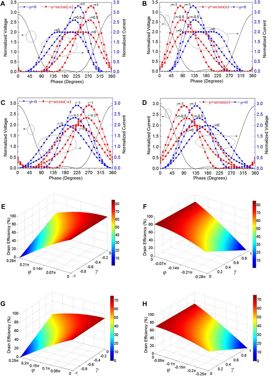
FIGURE 1. Theoretical voltage and current waveforms and drain efficiency. (A–D) Theoretical voltage and current waveforms when φ = arctan(-α), φ = 0, φ = arctan(α). (A)α = 43/37, β = 6/37, and φ
The DC and RF power of the PA can be calculated using the following expressions: Eqs 12 and 13. The drain efficiency (DE) of the modified hybrid inverse continuous modes can be calculated based on Eqs 3, 6, 12, and 13 as follows:
Using the above expression, the DE which is defined as the ratio of PRF to Pdc can be written as follows:
The DE of the hybrid inverse continuous mode PA, which depends on γ, α, and φ, can be clearly found from the above expression. According to the relation between γ and φ and the range of γ, α, and φ, DE will decrease with the increase in the absolute value of φ. By calculating, it is concluded that when the DE is greater than 60%, the range of γ will be reduced with the increase in the absolute value of φ and when α = 1 and α = 43/37, the corresponding relations for the theoretical DE are plotted in Figures 1E,F, respectively. Figure 1E shows DE at the boundary values of α = 43/37, β = 6/37, and φ ≥ 0. When φ = 0, the amplifier has a maximum DE of 82.17%, and the DE does not change with the γ. With the increase in φ, the DE decreases gradually. At the same time, the DE will decrease with the decrease in γ. The maximum value of DE also appears at φ = 0, as shown in Figure 1F. As the absolute value of φ increases, the DE decreases. When φ has a fixed value, the DE will also decrease with the increase in γ. Figure 1G,H show DE at the boundary values of α = 1 and β = 0. The DE has a similar variation law to those in Figure 1E,F.
In order to obtain the design space of the fundamental and second harmonic admittances for DE over 60%, the expressions in Eqs 8, 9, 11, and 14 must be combined. Figure 2B shows the fundamental and second harmonic design spaces for a = 1, a = 9/8, and a = 43/37. It can be seen from Figure 2B that the fundamental admittance space is a large continuous region, which improves the sufficient design space for us to design broadband power amplifiers. In addition, the second harmonic admittance has a completely new region compared with the traditional inverse continuous type, and the efficiency of the amplifier can be further improved by controlling the harmonic component.
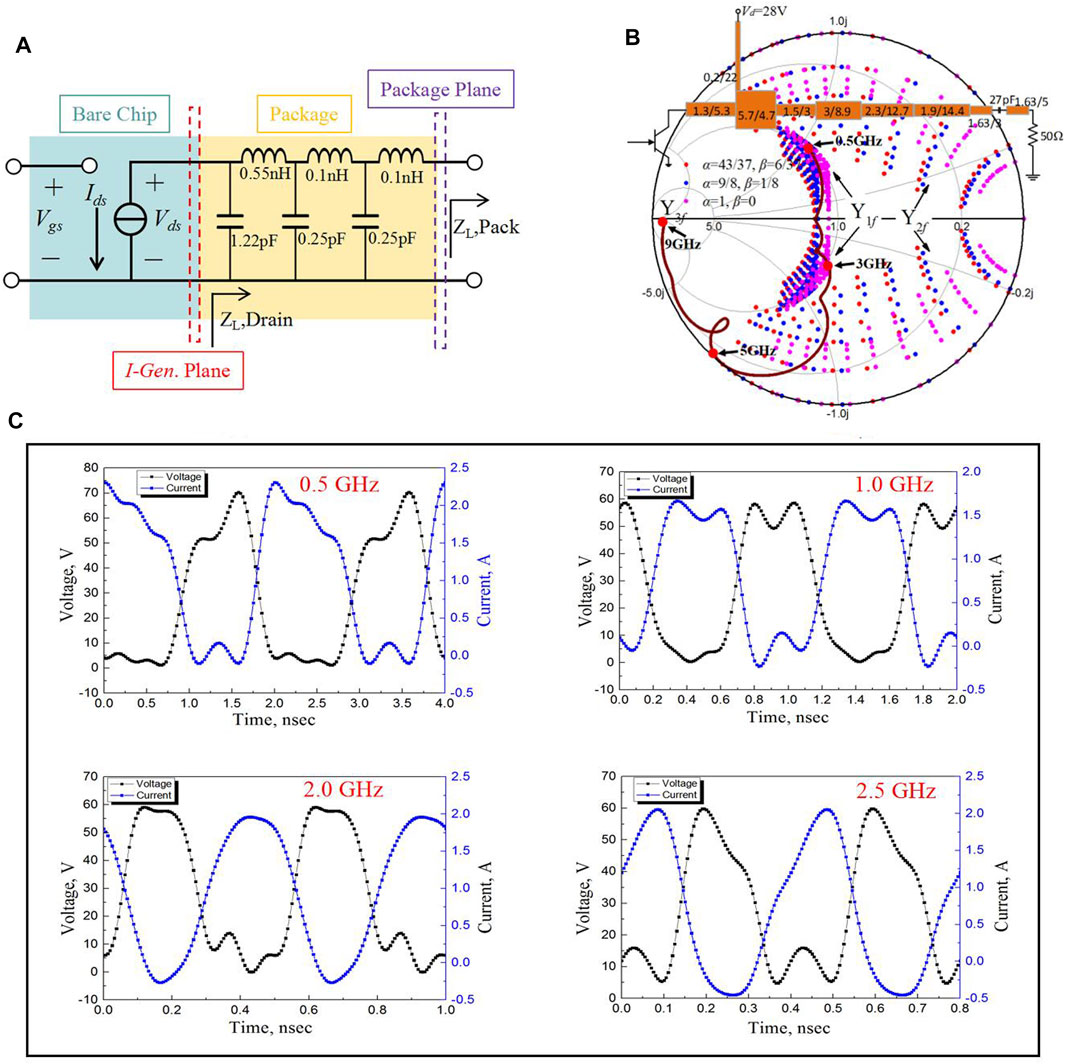
FIGURE 2. (A) Equivalent circuit model of transistor modeling showing the parasitics. (B) Output matching network and the admittances at the intrinsic drain plane. (C) De-embedded voltage and current waveforms of the PA at the I-gen plane.
Realization and Experimental Results
Output Network and Output Waveform
A 10-W Cree CGH40010F GaN HEMT packaged device was used for implementation. An ultra-wideband high-efficiency PA is designed to prove the theory proposed in this study. As the theoretical PA mode analysis refers to the intrinsic drain plane (I-generation plane), the parasitics of the transistor need to be properly modeled. Hence, computer-aided design (CAD)-based modeling can be performed in combination with bare sheet models and encapsulation models, which are provided by the manufacturer [25]. The typical equivalent-circuit model of this transistor is shown in Figure 2A, indicating the intrinsic and package parasitics [26].
The output matching network with the dimensions of transmission lines and the admittances at the intrinsic drain plane are shown in Figure 2B, where the fundamental impedance is consistent with the results obtained from the previous analysis. However, since the bandwidth of the PA exceeds one octave, the second harmonic admittance does not fully enter the ideal space. As a result, the efficiency of the PA will be affected before 1.5 GHz. In other words, the efficiency of the PA will be increased after 1.5 GHz. Additionally, when the frequency is higher than 2.5 GHz, the efficiency of the PA will decrease significantly.
To verify the operating mode of the designed PA, the simulated voltage and current waveforms at the intrinsic drain plane are investigated using the harmonic balance simulator available in ADS. Figure 2C shows the simulated voltage and current waveforms when the PA is operating at 0.5, 1.0, 2.0, and 2.5 GHz, respectively. The voltage and current waveforms are basically in agreement with those of the hybrid continuous inverse power amplifiers. The drain voltage is set to 28 V with a quiescent current of 62 mA.
Amplifier Circuit Fabrication and Testing
The circuit is fabricated on Rogers’s RO4350B with εr = 3.66 and H = 0.762 mm. The photograph of the proposed PA is presented in Figure 3A. The PA is first tested under the stimulus of a single-tone continuous wave signal from 0.5 to 2.5 GHz with a step of 0.1 GHz. The drain bias voltage and the gate bias voltage of the transistor are both set to the value that causes the best drain efficiency (DE) in the test.
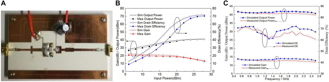
FIGURE 3. (A) Photograph of the proposed PA. (B) Simulated and measured drain efficiency, output power, and gain virus input power at 0.8 GHz. (C) Simulated and measured drain efficiency, output power, and gains of the designed PA.
The simulated and measured gain, drain efficiency, and output power of the designed amplifier versus the input power at 0.8 GHz are shown in Figure 3B. The simulated and measured results of the output power, drain efficiency, and gain of this PA over the entire frequency band are given in Figure 3C. The simulated and measured results show that the drain efficiency can reach more than 60% in the frequency range of 0.5–2.5 GHz (relative bandwidth 133%). The test results of drain efficiency are 60.7–71.5%. Over the same band, the measured output power from 39.8 to 41.9 dBm is obtained. The gain is 11.8–13.9 dB within the same frequency band. In addition, the simulation results of gain and output power are in good agreement with the measured results due to the EM simulation of the layout in the ADS. It can be seen from Figure 3C that the drain efficiency of the amplifier fluctuates in the operating frequency range. The reason is that the operating bandwidth of the amplifier is very wide, the operating modes of different frequencies are different, and the efficiency of different operating modes is different, so the drain efficiency of the amplifier will fluctuate in the entire frequency range.
Compared with the previous design, the proposed PA designed in this study has wider bandwidth, higher drain efficiency, and stable output power, as shown in Table 1.
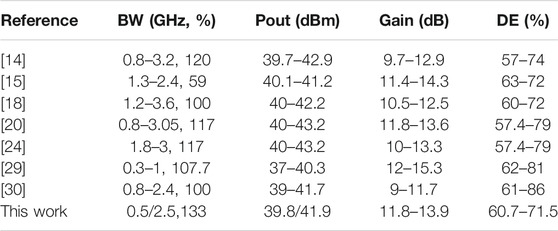
TABLE 1. Comparison with recently reported broadband PAs.
Conclusion
A high-efficiency and wideband hybrid continuous invert PA with phase shift parameters is presented in this article, the current equation of which has been rebuilt to gain greater design space. It is shown that the fundamental and second harmonic admittances change with the introduction of the phase shift parameters. On the basis of this theory, the drain efficiency of the designed PA is 60.7–71.5% and the output power is 39.8–41.9 dBm.
Data Availability Statement
The original contributions presented in the study are included in the article/Supplementary Material; further inquiries can be directed to the corresponding author.
Author Contributions
CN developed the concept and supervised the whole project. JL carried out the simulations. CN and HW analyzed the simulation data. JL designed the structure and fabricated the sample. ZZ and LZ performed the experiments. CN and JL contributed to writing and finalizing the manuscript. JZ perfected the final manuscript. MC contributed to manuscript revision and language editing. All authors participated in the discussion of the results.
Funding
This work was supported in part by the Key Natural Science Projects in the Education Commission of Anhui Province (Grant no. KJ2020A0105), in part by the Project of Anhui Province Key Laboratory (Grant no. 2019ZDSYSZY02), in part by the Research Project of the Provincial Research Platform of Hefei Normal University (Grant no. 2020PTZD10), and in part by the Anhui Science and Technology Project (Grant nos. 201904a05020061 and 202003a05020031). Anhui high education quality engineering Project (Grant no. 2020jyxm1576).
Conflict of Interest
The authors declare that the research was conducted in the absence of any commercial or financial relationships that could be construed as a potential conflict of interest.
References
Zheng SY, Liu ZW, Zhang XY, Zhou XY, Chan WS. Design of Ultrawideband High-Efficiency Extended Continuous Class-F Power Amplifier. IEEE Trans Ind Electron (2018) 65:4661–9. doi:10.1109/TIE.2017.2772163
Husna Hamza K, Nirmal D. A Review of GaN HEMT Broadband Power Amplifiers. Int J Electron Commun (Aeü) (2019) 116:1–11. doi:10.1016/j.aeue.2019.153040
Ding Y, Guo YX, Liu FL. High-efficiency Concurrent Dual-Band Class-F and Inverse Class-F Power Amplifier. Electron Lett (2011) 47:847–9. doi:10.1049/el.2011.1662
Negra R, Sadeve A, Bensmida S, Ghannouchi FM. Concurrent Dual-Band Class-F Load Coupling Network for Applications at 1.7 and 2.14 GHz. IEEE Trans Circuits Syst (2008) 55:259–63. doi:10.1109/TCSII.2008.918993
Sharma T, Darraji R, Ghannouchi F. A Methodology for Implementation of High-Efficiency Broadband Power Amplifiers with Second-Harmonic Manipulation. IEEE Trans Circuits Syst (2016) 63:54–8. doi:10.1109/TCSII.2015.2482139
Lu Z, Chen W. Resistive Second-Harmonic Impedance Continuous Class-F Power Amplifier with over One Octave Bandwidth for Cognitive Radios. IEEE J Emerg Sel Top Circuits Syst. (2013) 3:489–97. doi:10.1109/JETCAS.2013.2284615
Poluri N, De Souza MM. High-Efficiency Modes Contiguous with Class B/J and Continuous Class F $^{-1}$ Amplifiers. IEEE Microw Wireless Compon Lett (2019) 29:137–9. doi:10.1109/LMWC.2018.2886655
Du X, You CJ, Cai J, Helaoui M, Ghannouchi FM, Zhao Y, et al. Novel Design Space of Load Modulated Continuous Class-B/J Power Amplifier. IEEE Microw Wireless Compon Lett (2018) 28:156–8. doi:10.1109/LMWC.2017.2779883
Thian M, Barakat A, Fusco V. High-Efficiency Harmonic-Peaking Class-EF Power Amplifiers with Enhanced Maximum Operating Frequency. IEEE Trans Microwave Theor Techn. (2015) 63:659–71. doi:10.1109/TMTT.2014.2386327
Aldhaher S, Yates DC, Mitcheson PD. Modeling and Analysis of Class EF and Class E/F Inverters with Series-Tuned Resonant Networks. IEEE Trans Power Electron (2016) 31:3415–30. doi:10.1109/TPEL.2015.2460997
Liu S, Liu M, Yang S, Ma C, Zhu X. A Novel Design Methodology for High-Efficiency Current-Mode and Voltage-Mode Class-E Power Amplifiers in Wireless Power Transfer Systems. IEEE Trans Power Electron (2017) 32:4514–23. doi:10.1109/TPEL.2016.2600268
Yang Z., Yao Y, Liu Z, Li M, Li T, Dai Z. Design of High Efficiency Broadband Continuous Class-F Power Amplifier Using Real Frequency Technique with Finite Transmission Zero. IEEE Access (2018) 6:61983–93. doi:10.1109/ACCESS.2018.2875010
Steve CC, Paul JT, Alan LC, Jonathan L, Johannes B. On the Continuity of High Efficiency Modes in Linear RF Power Amplifiers. IEEE Microw Wirel Compon Lett (2009) 19:665–7. doi:10.1109/LMWC.2009.2029754
Wang J, He S, You F, Shi W, Peng J, Li C. Codesign of High-Efficiency Power Amplifier and Ring-Resonator Filter Based on a Series of Continuous Modes and Even-Odd-Mode Analysis. IEEE Trans Microwave Theor Techn. (2018) 66:2867–78. doi:10.1109/tmtt.2018.2819650
Saxena S, Rawat K, Roblin P. Continuous Class-B/J Power Amplifier Using a Nonlinear Embedding Technique. IEEE Trans Circuits Syst (2017) 64:837–41. doi:10.1109/tcsii.2016.2633300
Colantonio P, Giannini F, Giofrè R, Piazzon L. High-efficiency Ultra-wideband Power Amplifier in GaN Technology. Electron Lett (2008) 44:130–1. doi:10.1049/el:20083067
Cipriani E, Colantonio P, Giannini F, Giofrè R. Theoretical and Experimental Comparisons of Class F vs. Class F-1 PAs In Proc. Of EuMiC2010. Paris, France: IEEE (2010). p. 428–31.
Huang C, He S, Shi W, Song B. Design of Broadband High-Efficiency Power Amplifiers Based on the Hybrid Continuous Modes with Phase Shift Parameter. IEEE Microw Wireless Compon Lett (2018) 28:159–61. doi:10.1109/LMWC.2017.2787061
Tang Q, Li Y, Li W. Second Octave Power Amplifier Design Based on Resistive‐reactive Series of Continuous Inverse Modes. Electron Lett (2017) 53:510–2. doi:10.1049/el.2017.0044
Shi W, He S, Li Q, Qi T, Liu QA. Design of Broadband Power Amplifiers Based on Resistive-Reactive Series of Continuous Modes. IEEE Microw Wireless Compon Lett (2016) 26:519–21. doi:10.1109/LMWC.2016.2574823
Shariatifar M, Jalali M, Abdipour A. A Concurrent Dual-Band Continuous Class-F Power Amplifier with Intermodulation Impedance Tuning: Analysis and Design Technique. AEU - Int J Electronics Commun (2019) 111:152899–11. doi:10.1016/j.aeue.2019.152899
Cao T, Liu Y, Chen W, Yang C, Zhou J. Analytical Design Solution for Optimal Matching of Hybrid Continuous Mode Power Amplifiers Suitable for a High-Efficiency Envelope Tracking Operation. Electronics (2019) 8:621–12. doi:10.3390/electronics8060621
Liu G, Mu F, Qiu X, Leng Y, Peng X. Design of Broadband Power Amplifier Based on Continuous Class-F Mode with Frequency Parameterization. IEICE Electron Express (2019) 16:20190038. doi:10.1587/elex.16.20190038
Luo W, Tang Z, Ge B, Cao X. Design of Broadband Power Amplifier Based on a Series of Novel Continuous Inverse Modes. Electron Lett (2017) 53:685–7. doi:10.1049/el.2017.0674
Pengelly R, Millon B, Farrell D, Pribble B, Wood S. Application of Non-linear Models in a Range of Challenging GaN HEMT Power Amplifier Designs. Atlanta, GA, USA: Presented at the IEEE MTT-S Int. Microw. Symp (2008).
Paul JT, Johannes B. Waveform Inspired Models and the Harmonic Balance Emulator. IEEE Microwave Mag (2011) 12:38–54. doi:10.1109/MMM.2010.940101
Shi W, He S, Li Q. A Series of Inverse Continuous Modes for Designing Broadband Power Amplifiers. IEEE Microw Wireless Compon Lett (2016) 26:525–7. doi:10.1109/lmwc.2016.2574820
Li QR, He SB, Dai ZJ. Design of Broadband High-Efficiency Power Amplifiers Based on the Hybrid Continuous Inverse Mode. San Francisco, CA, USA: IEEE MTT-S Int. Microw. Sym. (IMS) (2016).
Sepehr ZH, Mohsen H, Marian KK, Hiroo S. Continuous Class-F Power Amplifier Using Quasi-Elliptic Low-Pass Filtering Matching Network. IEEE Trans Circuits Syst Exp Briefs (2020) 67:2407–11. doi:10.1109/TCSII.2020.2964895
Keywords: broadband, high-efficiency, continuous mode, power amplifier, second harmonic admittance
Citation: Ni C, Wang H, Liu J, Chen M, Zhang Z, Zhang L, Zhu J and Wu X (2021) A Broadband High-Efficiency Hybrid Continuous Inverse Power Amplifier Based on Extended Admittance Space. Front. Phys. 9:648127. doi: 10.3389/fphy.2021.648127
Received: 31 December 2020; Accepted: 21 June 2021;
Published: 15 July 2021.
Edited by:
Lei Guo, The University of Queensland, AustraliaReviewed by:
Guohua Liu, Hangzhou Dianzi University, ChinaNgocDuc Au, Soongsil University, South Korea
Copyright © 2021 Ni, Wang, Liu, Chen, Zhang, Zhang, Zhu and Wu. This is an open-access article distributed under the terms of the Creative Commons Attribution License (CC BY). The use, distribution or reproduction in other forums is permitted, provided the original author(s) and the copyright owner(s) are credited and that the original publication in this journal is cited, in accordance with accepted academic practice. No use, distribution or reproduction is permitted which does not comply with these terms.
*Correspondence: Chun Ni, chunni_hfnu@sina.com