Monolithic arrays of silicon sensors
 Ian Harding
 Wei Chen
 Gabriele Giacomini
 Anthony Kuczewski
 - Brookhaven National Laboratory, Upton, NY, United States
Monolithic arrays of silicon p-n junctions are commonly used to deliver spatial information on impinging radiation, with the advantages of low-noise and fast signal generation. Additionally, array geometries also allow for a segmentation of a large area into individual channels that can be read out in parallel, so that a high-event rate can be managed. To optimize the noise performance, however, some key points must be addressed to control the silicon/silicon oxide interface. Replacing the p-n junctions with silicon drift sensors avoids noise related to the interface states, at the expense of a more complicated process and slower signals. In this paper, some of the aspects needing consideration when engineering a monolithic array of silicon sensors are reviewed.
1 Introduction
Silicon is extensively used as a semiconductor material for radiation detecting sensors for a number of reasons. First, decades of commercial silicon-based integrated circuit development has lead to the capability of growing large-volume, low-defect, high-quality single-crystal material at relatively low cost while also paving the way for mature and readily available processing technology. Moreover, silicon detectors can operate close to room temperature, have a low Fano factor [1] which makes them useful for spectroscopy, and their sensitivity to charged particles and photons has a huge energy range - spanning from infrared to gamma rays. Its oxide (SiO2), thermally grown in dedicated furnaces in clean rooms, is of exceptional quality, providing insulation and protection of the substrate and can survive subsequent aggressive processing steps (as a counterexample, germanium oxide is soluble in water, limiting the processing options for germanium-based devices). While SiO2 is transparent to UV (its bandgap is larger than the energy of UV light), it can act as anti-reflective coating, alone or in association with nitrides or other dielectrics for light sensing applications [2]. SiO2 is characterized by a positive charge, usually present at the interface between silicon and SiO2 as well as within the oxide itself, which ranges from about 1010 cm−2 in 100 oriented wafers to on the scale of 1011 cm−2 for 111 wafers (these being the two mostly used crystal orientations) [3]. This oxide charge induces an electron accumulation layer at the Si/SiO2 interface that can create issues for detector performance if not properly treated.
Another reason for the success and broad use of silicon as the starting material for sensors is the possibility of finely patterning the electrodes to achieve either spatial information or to have independent sensitive units on the same substrate, therefore removing any dead areas at the edges of each of the sensing elements. The former allows for devices with a spatial resolution on the scale of 1 μm, the latter allows for a high acquisition rate when the electrodes are read out by independent electronic channels in parallel. In Figure 1 we show some typical ways to pattern the electrodes: pixels, microstrips, and pads.
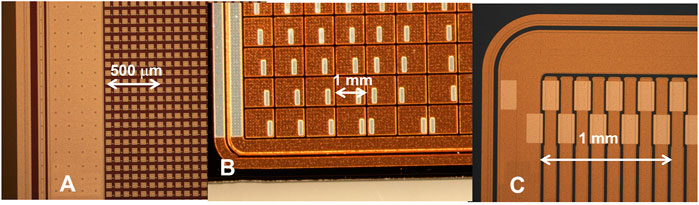
FIGURE 1. Examples of monolithic silicon sensor arrays fabricated by BNL: (A) silicon pixel sensor (55 μm pitch), (B) corner of the Maia silicon pad sensor (1 mm pitch, for high rate fluorescence spectroscopy), and (C) silicon strip sensor (120 μm pitch).
The advantages of the monolithic approach are evident: ease of assembly, exploitation of effects such as signal sharing to increase the spatial resolution, and almost unity fill factor. However, we must also consider some characteristics that make the arrays prone to a decrease in performance or even failure, as detailed in the sections below.
In the following sections, we make use of the TCAD numerical simulator SILVACO1 to support experimental findings and to help visualize the physical quantities that play a critical role in the behaviour of a device. It is good practice for the designer to perform simulations prior to the actual device fabrication, to address and even discover key points in the functioning of the detector.
2 Isolation of electrodes
2.1 n + electrodes
The electron accumulation layer induced by the positive charge in the oxide will short n + electrodes unless a compensating p-doped layer is used to interrupt it. Usually, one of two types of layer is used: p-spray [4] or p-stop [5]. A p-spray layer is formed through a low dose boron implant, typically on the scale of 1012cm−2, which is done at the beginning of the device process on a blank oxidized silicon wafer. In the following, we make use of a simple TCAD simulated structure, a silicon microstrip sensor partially shown in Figure 2. This particular geometry features a pitch of 100 μm, a gap between implants of 40 μm, a substrate thickness of 200 μm with a doping concentration of 1 × 1012 cm−3 to which a reverse bias of 100 V has been applied. The oxide charge density is 1 ⋅ 1011 cm−2, unless specified otherwise. Figure 2 refers to a structure with p-type substrate and n + electrodes on top, with p-spray, and it shows a schematic of the electron concentration and the electric field at the Si/SiO2 interface with the p-spray layer. Note that in the case of a p-type substrate, the interface is populated by holes from the boron doping. The p-spray is laterally depleted at the junction with the n-electrode, which creates the largest electric field value in the whole substrate.
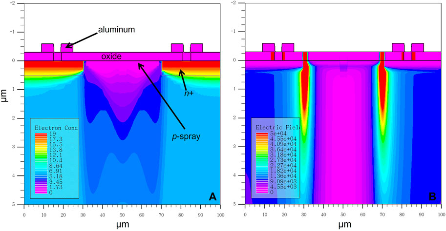
FIGURE 2. 2D TCAD simulations of (A) electron concentration (cm−3, log scale) and (B) electric field (V/cm, linear scale) maps in an example of a n-on-p sensor with p-spray. Red (violet) color maps high (low) -value regions for that quantity. The highest electric fields develop at the junction p-spray/n-implant.
The p-stop implantation is a patterned boron implantation which can be performed later in the device fabrication process and is generally more implanted than the p-spray. In this case, the electron accumulation layer extends from the n + electrode to the p-stop, and it is laterally depleted by the voltage difference present between the n + electrode and the floating p-stop, as seen in Figure 3. Contrary to the case of the p-spray layer, the highest electric fields are at the junction of the p-stop implantation and the accumulated electrons, which are ohmically connected to the n + electrode. In either case, the designer of such a device must evaluate the critical points for breakdown, which happens at the junction of the p-layer and the n-layer (either electron accumulation layer of phosphorus implant). To make a smoother electric field, the implantation layer can be made deeper by means of higher energy implantation and more rounded through longer annealing [6].
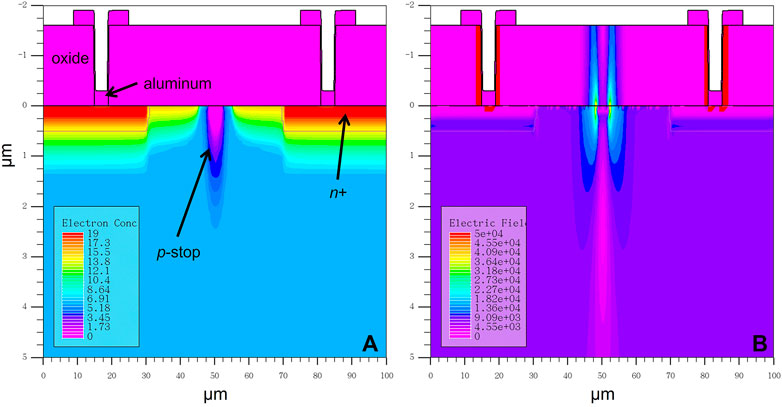
FIGURE 3. 2D TCAD simulations of (A) electron concentration (cm−3, log scale) and (B) electric field (V/cm, linear scale) maps in an example of a n-on-p sensor with p-stop. Red (violet) color maps high (low) -value regions for that quantity. The highest electric fields develop at the junction p-stop/electron accumulation layer.
However, in practice, these devices are more complicated than the simulations above. Specifically, these models do not account for the electrostatic state of the oxide surface which is exposed to air or vacuum. At the top side of the oxide, a layer formed by ions from the environment and by electrons from the contacts will slowly build up and create a high-resistive film, a gate, equipotential to the electrodes which are kept at the read-out electronics input voltage (Figure 4) [7,8]. Thus the correct way to model a silicon sensor under operating conditions is by simulating a grounded gate extended across the oxide (Figure 4B) and equipotential to the adjacent electrodes.
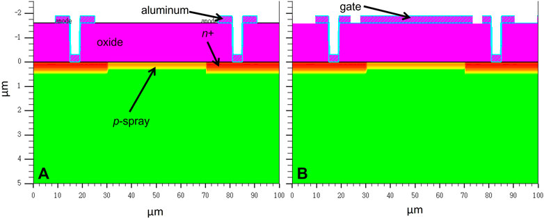
FIGURE 4. (A) Standard geometry used in TCAD simulations of an n-on-p sensor and (B) the same structure under stable conditions, i.e., with a gate equipotential to the electrodes, and placed over the external surface of the sensor to simulate the electrostatics of the silicon/silicon oxide interface after prolonged exposure to the environment.
In the present case of n + electrodes, the gate is positive with respect to the substrate (which being p-type is at negative voltage) and attracts electrons at the interface, as the oxide charge does. We can expect a slightly higher electric field at the p-stop/electron layer junction (as the concentration of electrons increases) and a slightly lower electric field at the p-spray/n + interface (as the p-spray is slightly depleted by the excess of electrons). Effects are expected to be generally small. Nevertheless, it is good practice to simulate the electrostatic in the final conditions, that depends on the substrate and oxide thickness, on the applied voltage, and on the overall geometry. This is much more important in p + electrodes, as explained in the following subsection.
2.2 p + electrodes
Next, let us consider p + electrodes on an n-type substrate.
Due to the positive charge trapped in the Si/SiO2 interface, one expects an electron accumulation layer at the non-implanted interface (gap between pixels), and thus p + pixels should always be insulated. However, as in the n + electrodes above, the fields are more complicated than this approximation. During operation, a gate builds at the outermost surface of the oxide (considering the oxide impermeable to charges) and this gate, with the prolonged application of bias, stays at the voltage of the electronics (nearby metals). This leads the interface to be either in accumulation, inversion, or depletion [9].
In accumulation, the system is similar to the basic model where the positive charge of the oxide creates a layer of electrons at the interface that can lead to noise. Conversely, the case of inversion is worse-the concentration of holes at the interface is larger than that of the electrons which creates parasitic resistance between neighbouring pixels and the noise is relatively high [3]. The last case, depletion, has the lowest relative capacity but has relatively higher leakage along the interface. Therefore, stable silicon devices operate with either a depleted or accumulated interface. The particular state of operation is dependent on a number of factors, including the array geometry, the doping concentration of the substrate, and the flat-band voltage of the Si/SiO2/gate system, where the flat-band voltage of a metal-oxide-semiconductor system is defined as: VFB = −Qox/Cox, where Qox is the charge densities into the oxide and Cox is the capacitance per unit area.
In Figure 5, we show the effect of three different charge densities into the oxide: 1 × 1010 cm−2, 3 × 1011 cm−2 and 1 × 1012 cm−2 which correspond to the cases of 100-oriented wafers, 111-oriented wafers, and after irradiation, respectively. The simulated geometry is similar to that of Figure 4, but with p + electrodes on an n-type substrate and without any p or n-spray. For a 1 μm oxide, the flat-band voltage for each of the three cases is 0.5, 15 and 48 V, respectively. As can be seen, for this particular geometry and for the applied bias voltage (100 V), the device works in inversion, depletion, and accumulation respectively. As was studied in [9], even a system characterized by a high flat-band voltage, as is 48 V in this example, can work with an interface depleted if a suitable high bias voltage is applied. This voltage, however, may be too high to be viable and the designer seeking best noise performance should tune the oxide thickness - given an oxide charge - as to have a flat-band voltage in the correct range to have depletion at a low-enough bias voltage. There is no analytical formula that predicts the maximum flat-band voltage to have depletion, and so TCAD simulations need to be performed for any specific substrate and electrode geometry.
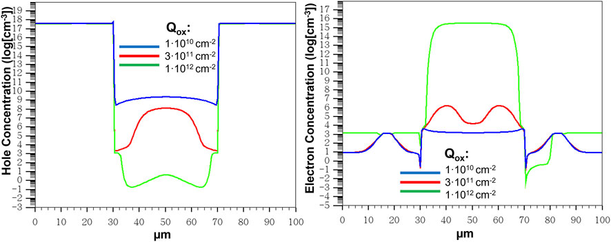
FIGURE 5. (A) Cutline at Y = 0 (i.e., at the interface silicon/silicon oxide) of the hole and (B) electron concentration for the geometry in Figure 4 and p + electrodes on n-type substrate (no spray). Charge into oxide is 1 × 10¹⁰, 3 × 10¹¹, or 1 × 1012 cm−2, as specified in the legends. Oxide thickness is 1 μm, Vbias = 100 V. Notice how the interface goes to (weak) inversion (red curve), depletion (green curve) or accumulation (blue curve) according to the oxide charge density, even without the presence of any spray.
It is increasingly difficult to purchase 111 wafers, and so 100 wafers are becoming standard. This crystallographic interface has a lower charge density, and to compensate for the accompanying lower charge into the oxide, charge is inserted into the device by ion-implanting a blank, uniform, low-dose phosphorus implant at the beginning of the process (“n-spray”). The n-spray introduces free electrons that simulate the accumulated electrons usually present at the Si/SiO2 interface in 111 wafers, and once the n-spray gets partially or totally depleted, the ionized phosphorus atoms simulate the positive charge within.
A good example of this situation is the Maia detector [10,11]. Maia is an array of 384 p-on-n pads at a pitch of 1mm, and it is used for X-ray spectroscopy in fluorescence experiments at synchrotron beamlines. Every pad is independently wire-bonded to a channel of a low-noise front-end electronics placed at the edge of the sensor itself. It consists therefore of almost 400 channels, read-out in parallel for an extremely high event throughput. Its noise has to be as low as possible, so the interface must be depleted during operation. To achieve this, as the Maia sensor was fabricated on 100 high-resistivity silicon substrates with oxide charge on the order of 1010 cm−2, an additional oxide charge was simulated by an n-spray implant with an implanted dose of 2 × 1011 cm−2, and the oxide thickness tuned after performing TCAD simulations so that the VFB sits between 5 and 10 V. A way to speed up the stabilization and the building up of the gate over the oxide can be to artificially introduce some moisture in the system by fluxing nitrogen through deionized water.
3 Sources of noise and signal losses
3.1 Noise from resistive layers
While critical to preventing shorting between pixels, p-spray and p-stop are found to introduce additional noise to the detector system. Besides the obvious increase in capacitance, which makes series and flicker noise more important (see section below), they are a source of Johnson (thermal) noise as they are resistive layers. This noise is capacitively coupled to the electrodes and has a particular frequency dependence that can be deduced by measuring the noise of the system as a function of the shaping time. For example, the strip detector considered in [12] was measured by a low-noise charge preamplifier and Johnson noise from p-stop was the main source of noise for a certain range of shaping times; notably, strip sensors with different geometry but fabricated on the same wafer (therefore sharing technology) showed a small effect on the noise due to this contribution even with the same read-out electronics.
Another non-standard source of noise is induced by the continuity of resistive layers such as n/p-spray or electron accumulation layers and has been observed in strip sensors [13]. We remark the fact that the continuity is necessary to have such noise, and the presence of these layers, say, in between the strips only and interrupted at the strip tip, does not give origin to this noise. This noise, having a peculiar noise dependence of
While these sources of noise cannot be completely avoided, it is important for the designer to be aware of them and possibly to find strategies to mitigate them.
3.2 Capacitance
The overall noise of the system is strongly affected by the capacitance, as series noise and 1/f noise are linearly dependent on it. As read-out is based on CMOS ASICs, 1/f noise usually is the dominant noise term. Furthermore, as modern read-out electronics are read out fast with short shaping times, series noise also plays an important role. The capacitance of one electrode towards the backside Cback can be roughly estimated by the parallel plate approximation:
where d is the depleted substrate thickness and A is the electrode area. In Figure 6, we see the results of a few 2-dimensional TCAD simulations of the capacitance of the cell depicted in Figure 2 for different substrate thickness with and without n-spray. As it can be seen, capacitance towards the backside scales inversely with the thickness [14].
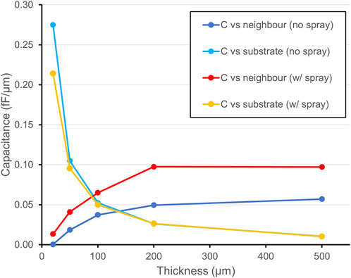
FIGURE 6. 2D TCAD simulations of the capacitance/micron towards the neighbour and toward the backside vs. thickness, with or without spray between the electrodes. 2D geometry is the one of Figure 4A. Frequency is 100 kHz. The capacitance towards the back is unaffected by the presence of a spray and is given by the parallel plane capacitor formula in Eq. 1; interstrip capacitance is less important in thin devices.
However, we must also consider the capacitance towards the neighbouring pixels, which can in fact be dominant with respect to the parallel plate value. For devices fabricated on thin substrates, such as LGADs (20–50 μm), the capacitance towards the neighbours is in fact negligible. In such devices, the back acts as an electrostatic shield that terminates the electrostatic lines, suppressing the capacitance towards the neighbours. On the other hand, it is known that for silicon microstrip detectors, whose standard thickness is 200–300 μm, the inter-strip capacitance dominates [15]. In Figure 6, the non-negligible contribution of a resistive layer in between the strips is shown. The resistive layers facilitate the coupling and therefore increase the inter-electrode capacitance, while leaving unaffected the capacitance towards the back.
As a further example, n-strips separated by p-spray have a capacitance which can be a factor of two or more larger: care must be taken during the phase of the development to calibrate the dose of the resistive layer as to limit the increase in capacitance [15].
Inter-electrode capacitance feeds the noise from neighbouring channels as well [16]. However, in a cluster of n strips, the overall noise is not
3.3 Charge sharing
If an ionizing event occurs in the gap between the implants, one would expect that the charge generated by the interaction to distribute among the nearby electrodes. For devices with read-out electronics sensitive enough to measure the amount of charge collected by each electrode with good enough resolution, it is possible to reconstruct with enhanced accuracy the hit position. However, if the collected charge falls below the threshold for detection, the event is not detected and the sensor loses efficiency.
A dramatic example of this is provided by pixel detectors for high energy physics. If the volume in-between the implants is fully sensitive before irradiation, after irradiation when the amount of charge collected is less (due to loss of signal due to charge trapping and recombination) and the noise increases (mainly due to the increase of the leakage current due to radiation damage), a certain loss of spacial efficiency at the interpixel regions is experienced [18].
There are applications when charge sharing has to be avoided, for example when channels need to be independent and position resolution is not an output of the system. One such example is the Maia microprobe array, which is used for high rate X-ray spectroscopy. The Maia utilizes a molybdenum mask to collimate the active area of pixels by absorbing X-rays that would hit the sensor in the region between the pixels.
3.3.1 Case study: LGADs
The charge sharing is particularly critical is the case of array of Low-Gain Avalanche Diodes (LGADs) [19], recently proposed as timing detectors for the ATLAS [20] and the CMS [21] experiments at CERN, as it leads to signal loss. In LGADs, a Junction Termination Edge [22] is placed at the border of the pad to protect the device from premature breakdown. A simple TCAD simulation of the electrostatic of the region of the gap reveals that signal electrons generated into the substrate below the JTE and in gap region drift towards the JTE and do not experience any multiplication and therefore signals here are below the threshold for detection. The gap and the JTE border of LGADs are therefore dead area and large pitches are necessary to have a decent fill factor [23] (Figure 7).
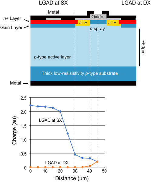
FIGURE 7. Sketch of the border region of a typical LGAD and plot of the charge collected by the two LGADs as function of the impinging point of a mip crossing vertically the silicon chip. The data points in the plot are obtained by mean of TCAD simulations.
4 Arrays of silicon drift detectors
In high rate spectroscopic applications, it is convenient to replace the array of PIN diodes with an array of Silicon Drift Detectors (SDD) (Figure 8). In this set-up, the capacitance at the input node is dominated by the anode capacitance towards the first ring, which is a few tens of femtofarads. The anode is as small as possible to be compatible with the interconnection method (for example, about 100 μm in diameter to allow for wire bonding, or tens of microns for bump-bonding). The capacitance towards the neighbours is suppressed, and so the noise coming from the other channel read-out is minimized and higher throughput possible (faster shaping times). For example, the measured energy resolution is 250 eV at 2 μm for the standard pin-based Maia [24] and 180 eV at 1 μs with the Maia SDD (called Hera) (David. P. Siddons, personal communication). Additionally, for SDD devices, the system is stable immediately after turn-on as the interface between anode and first ring (about 10 μm distance) can be in either state (depletion or accumulation), though most likely in depletion, due the high voltage difference applied between anode and first ring (10/20 V), which falls in a few microns. While the area outside the first ring is not that important, it is a good practice to keep it stable. This can be accomplished by avoiding exposing non-implanted silicon to the open air, where the potential is not defined. The outermost oxide surface should be either implanted or covered by metal. In Figure 8, there are only small non-implanted parts exposed to air, and as such the system proved stable.
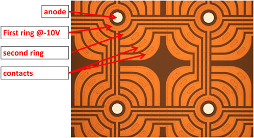
FIGURE 8. Microscope view of four pixels of Hera (pitch = 1 mm), a Silicon Drift Detector array replacing the pin-based array Maia. Brownish color is due to the polymide passivation. Details of the structure are indicated by arrows.
5 Conclusion
Technology maturity of silicon processing allows large area, monolithic arrays of silicon sensors to be fabricated. However, there are effects that must be considered for best performance. Such effects originate from the status of the silicon/silicon oxide interface in the gap in-between the electrodes. In this paper, the role of this interface on the noise in silicon-based radiation sensors is reviewed and discussed, including considerations for the effect of implantation in between pixels, charge sharing between pixels, and capacitance towards neighbouring pixels. When timing is not an issue and the best spectroscopic performance is sought-after, the deployment of silicon drift detectors in place of standard PIN diodes adds the advantage of an intrinsically stable detector.
Author contributions
IH wrote the paper in conjunction with GG, WC, and AR fabricated in the clean room most of the devices, AK performed the functional measurements on the devices, DS was responsible for the Maia project.
Funding
This material is based upon work supported by the US. Department of Energy under grant DE-SC0012704. This research used resources of the Center for Functional Nanomaterials, which is a US. DOE Office of Science Facility, at Brookhaven National Laboratory under Contract No. DE-SC0012704.
Acknowledgments
The authors wish to thank their colleagues at Brookhaven National Laboratory: Ronald Angona and Sean Robinson. They are indebted to Christopher Platte (University of Michigan in Ann-Arbor) for help in simulations.
Conflict of interest
The authors declare that the research was conducted in the absence of any commercial or financial relationships that could be construed as a potential conflict of interest.
Publisher’s note
All claims expressed in this article are solely those of the authors and do not necessarily represent those of their affiliated organizations, or those of the publisher, the editors and the reviewers. Any product that may be evaluated in this article, or claim that may be made by its manufacturer, is not guaranteed or endorsed by the publisher.
Footnotes
References
1. Lutz J, Schlangenotto H, Scheuermann U, De Doncker R. Semiconductor power devices. Berlin, Heidelberg: Springer Berlin Heidelberg (2011). doi:10.1007/978-3-642-11125-9
2. Acerbi F, Paternoster G, Capasso M, Marcante M, Mazzi A, Regazzoni V, et al. Silicon photomultipliers: Technology optimizations for ultraviolet, visible and near-infrared range. Instruments (2019) 3:15. doi:10.3390/instruments3010015
3. Giacomini G, Bosisio L, Rashevskaya I. Insulation issues in punch-through biased silicon microstrip sensors. IEEE Trans Nucl Sci (2016) 63:422–6. doi:10.1109/TNS.2015.2514195
4. Piemonte C. Device simulations of isolation techniques for silicon microstrip detectors made on p-type substrates. IEEE Trans Nucl Sci (2006) 53:1694–705. doi:10.1109/TNS.2006.872500
5. Unno Y, Kohriki T, Kondo T, Terada S, Ohsugi T, Iwata Y, et al. Novel p-stop structure in n-side of silicon microstrip detector. Nucl Instr Methods Phys Res Section A: Acc Spectrometers, Detectors Associated Equipment (2005) 541:40–6. doi:10.1016/j.nima.2005.01.036
6. Ghandhi SK. Semiconductor power devices: Physics of operation and fabrication technology. New York: Wiley (1977).
7. Longoni A, Sampietro M, Strueder L. Instability of the behaviour of high resistivity silicon detectors due to the presence of oxide charges. Nucl. Instr. Methods Phys. Res. A (1990):35–43.
8. Grove AS. Physics and technology of semiconductor devices. New York Chichester Brisbane [etc.]: J. Wiley and sons (1967).
9. Giacomini G, Chen W, Kuczewski A, Rumaiz AK, Siddons DP. Operational conditions of silicon pixel arrays for X-ray spectroscopy. IEEE Trans Nucl Sci (2019) 66:2245–51. doi:10.1109/TNS.2019.2943067
10. Siddons DP, Kirkham R, Ryan CG, De Geronimo G, Dragone A, Kuczewski AJ, et al. Maia X-ray microprobe detector array system. J Phys : Conf Ser (2014) 499:012001. doi:10.1088/1742-6596/499/1/012001
11. Ryan CG, Siddons DP, Kirkham R, Li ZY, de Jonge MD, Paterson DJ, et al. Maia X-ray fluorescence imaging: Capturing detail in complex natural samples. J Phys : Conf Ser (2014) 499:012002. doi:10.1088/1742-6596/499/1/012002
12. Giacomini G, Bosisio L, Rashevskaya I, Starodubtsev O. Noise characterization of double-sided silicon microstrip detectors with punch-through biasing. IEEE Trans Nucl Sci (2011) 58:569–76. doi:10.1109/TNS.2011.2107749
13. Giacomini G, Bosisio L, Rashevskaya I. Measurement of Johnson noise induced by p-stops in silicon microstrip detectors. IEEE Trans Nucl Sci (2013) 60:4022–5. doi:10.1109/TNS.2013.2276069
14. Giacomini G. Fabrication of silicon sensors based on low-gain avalanche diodes. Front Phys (2021) 9:618621. doi:10.3389/fphy.2021.618621
15. Rachevskaia I, Bosisio L, Potin S, Starodubtsev O. Test and quality control of double-sided silicon microstrip sensors for the ALICE experiment. Nucl Instr Methods Phys Res Section A: Acc Spectrometers, Detectors Associated Equipment (2004) 530:59–64. doi:10.1016/j.nima.2004.05.048
16. Spieler H. Semiconductor detector systems. Oxford; New York: Oxford University Press (2005). OCLC: 183673647.
17. Lutz G. Correlated noise in silicon strip detector readout. Nucl Instr Methods Phys Res Section A: Acc Spectrometers, Detectors Associated Equipment (1991) 309:545–51. doi:10.1016/0168-9002(91)90260-W
18. Weingarten J, Altenheiner S, Beimforde M, Benoit M, Bomben M, Calderini G, et al. Planar pixel sensors for the ATLAS upgrade: Beam tests results. J Instrum (2012) 7:P10028. doi:10.1088/1748-0221/7/10/P10028
19. Pellegrini G, Fernández-Martínez P, Baselga M, Fleta C, Flores D, Greco V, et al. Technology developments and first measurements of Low Gain Avalanche Detectors (LGAD) for high energy physics applications. Nucl Instr Methods Phys Res Section A: Acc Spectrometers, Detectors Associated Equipment (2014) 765:12–6. doi:10.1016/j.nima.2014.06.008
20. Collaboration A. Technical design report: A high-granularity timing detector for the ATLAS phase-II upgrade. In: Tech. rep Geneva: ATLAS Collaboration (2020).
21.CMS Collaboration. A MIP timing detector for the CMS phase-2 upgrade. In: Tech. rep Geneva: CERN (2019).
22. Fernández-Martínez P, Flores D, Hidalgo S, Greco V, Merlos A, Pellegrini G, et al. Design and fabrication of an optimum peripheral region for low gain avalanche detectors. Nucl Instr Methods Phys Res Section A: Acc Spectrometers, Detectors Associated Equipment (2016) 821:93–100. doi:10.1016/j.nima.2016.03.049
23. Apresyan A, Xie S, Pena C, Arcidiacono R, Cartiglia N, Carulla M, et al. Studies of uniformity of 50 μm low-gain avalanche detectors at the Fermilab test beam. Nucl Instr Methods Phys Res Section A: Acc Spectrometers, Detectors Associated Equipment (2018) 895:158–72. doi:10.1016/j.nima.2018.03.074
Keywords: noise, silicon drift sensors, silicon radiation detectors, silicon strip sensors, silicon sensor
Citation: Harding I, Chen W, Giacomini G, Kuczewski A, Rumaiz AK and Siddons DP (2022) Monolithic arrays of silicon sensors. Front. Phys. 10:927776. doi: 10.3389/fphy.2022.927776
Received: 25 April 2022; Accepted: 08 July 2022;
Published: 09 August 2022.
Edited by:
Natale Demaria, National Institute of Nuclear Physics of Turin, ItalyCopyright © 2022 Harding, Chen, Giacomini, Kuczewski, Rumaiz and Siddons. This is an open-access article distributed under the terms of the Creative Commons Attribution License (CC BY). The use, distribution or reproduction in other forums is permitted, provided the original author(s) and the copyright owner(s) are credited and that the original publication in this journal is cited, in accordance with accepted academic practice. No use, distribution or reproduction is permitted which does not comply with these terms.
*Correspondence: Ian Harding, iharding@bnl.gov