Research on vertical GaN devices based on gradient Al components
 Yonghe Chen
 Ye Yang
 Jianghui Zhai*
 - Guangxi Key Laboratory of Precision Navigation Technology and Application, Guilin University of Electronic Technology, Guilin, China
A groove-gate power device with a linearly gradient Al composition P-type AlGaN superjunction (abbreviated as LG-SJCAVET) is proposed, which uses polarized P-type AlGaN material instead of the traditional P-type GaN buried layer, avoiding the technical bottleneck of achieving high-aspect-ratio P-type doping in GaN materials. Simulation results show that, under the same structural parameters, the breakdown voltage of LG-SJCAVET reaches 2954V, and the on-resistance is 1.669
1 Introduction
With the further need for high breakdown voltage, low on-resistance, good reliability, and suppression of current collapse in transverse gallium nitride (GaN) devices, GaN vertical power devices have become a hot topic at present [1–9]. In 2013 [10], Zhongda Li and T. Paul Chow designed an enhanced vertical device with a superjunction structure, in which the aperture width, buffer layer thickness, and superjunction width were 6
However, the contradictory relationship between breakdown voltage and on-resistance of power devices has been a very important research topic in the field of vertical devices, and it is difficult to achieve high concentration of P-type doping in traditional GaN-based vertical power devices, which also restricts the in-depth research of devices [13–15].
To address the above practical issues, we utilized simulation software to design GaN-enhanced devices and proposed a groove-gate type power device with a P-type AlGaN superjunction with a linearly graded Al composition (referred to as LG-SJCAVET). The device buffer layer is composed of P-type AlGaN and N-type GaN columns, where polarized doped AlGaN material is used for the P column instead of the traditional P-type GaN buried layer. This allows for high hole concentration without physical doping, avoiding the technical bottleneck of highly doped P buried layer vertical devices in traditional techniques. The combination of P and N columns increases the depletion region area, reduces the electric field peak problem around the gate, mitigates the problem of uneven electric field distribution, improves the voltage resistance performance of the device, and is simple to implement in the manufacturing process.
2 Materials and methods
This section proposes a groove-gate power device with a P-type AlGaN superjunction with a linearly graded Al composition. The LG-SJCAVET is a groove-gate structure and the device, from top to bottom, consists of an N-type GaN substrate, a buffer layer composed of linearly graded P-type AlGaN column and N-type GaN column, a P-type GaN current blocking layer (CBL), an N-type GaN channel layer, an AlGaN barrier layer, a Si3N4 passivation layer, and an HfO2 gate dielectric layer.
Figure 1 shows the schematic structure of traditional GaN-based vertical devices CONV, traditional GaN-based vertical device SJ-CAVET with a super-junction structure, and LG-SJCAVET with a linearly gradient Al composition structure based on a vertical device. Since the device is completely symmetrical left and right, only the left half of the device is shown. The difference between LG-SJCAVET and SJ-CAVET is that the P-type GaN column structure in the buffer layer of the latter is replaced by a P-type AlGaN column structure with a linearly gradient Al composition.
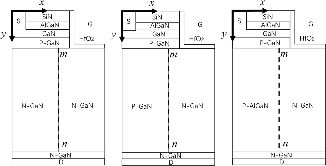
FIGURE 1. Structure diagram of CONV, SJ-CAVET and LG-SJCAVET.
CONV solves some of the problems existing in lateral devices, such as large leakage current, large device area, and uneven heating inside the device; SJ-CAVET solves the problem of smaller breakdown voltage of CONV by adding PN junction to the buffer layer to improve the voltage withstand characteristics of the device; and the new structure LG-SJCAVET solves the problem of difficult P-type doping existing in traditional devices, while having greater breakdown voltage.
During the simulation process, we introduced specific concentrations of N-type doping into the barrier layer, channel layer, and buffer layer to simulate unintentional doping introduced during material growth. The width, thickness, concentration, and Al component of the P-type AlGaN buffer layer are represented by the variables Wp, Tp, Np, and Xp, in that order, and the main structural parameters of the device are given in Table 1. A donor trap with a surface density of 5*1013 cm-2 and a level at 1.6 eV below the conduction band was also introduced at the interface between the passivation layer and the barrier layer to provide a two-dimensional electron gas at the heterojunction interface. A deep-level acceptor trap with a concentration of 1*1015 cm-3 and a level at 0.45 eV below the conduction band was introduced into the buffer layer to simulate the introduction of acceptor impurities during buffer layer growth.
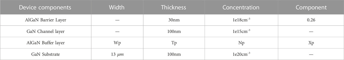
TABLE 1. LG-SJCAVET device main structure parameters.
The linear variation of Al composition in polarized-doped AlGaN along the growth direction results in a significant increase in the hole concentration and impurity activation rate inside AlGaN due to the polarization electric field. It also greatly enhances the thermal stability of the hole concentration [16].
Growing AlGaN along the negative y-axis direction on a GaN substrate, with the Al component increasing linearly from 0 to Xp, the spontaneous polarization and piezoelectric polarization increase with the increase of Al composition on the bottom surface of the AlGaN layer under the condition of constant thickness. The AlGaN material with gradient Al composition can be regarded as a crystal cell composed of several Al components increasing linearly from 0 to Xp, and the total polarization intensity inside the crystal cell is represented by a dipole moment. The intensity of the dipole moment in each crystal cell changes due to the gradual change in Al composition, which in turn leads to the gradual increase of the dipole moment along the positive y-axis and the formation of net polarization charges at the interfaces of adjacent crystal cells. Negative polarization charges in AlGaN material form a polarization field. In order to neutralize the polarization charges in AlGaN material, non-intentionally doped impurities with a concentration of 1*1015cm-3 are ionized under the effect of built-in polarization field, generating an equal number of holes. These holes, uniformly distributed in the AlGaN material due to the polarization effect, are called three-dimensional hole gas [17].
In the simulation software, the simulation environment temperature is set to 300K, and the physical model used in the simulation is based on the Ga-face polarity GaN material model with (0,001) crystal orientation. The default gate width of the device is 1
where
Figure 2 shows the electron concentration distribution near the groove gate during device turn-on and turn-off. As shown in Figure 2A, when the gate voltage Vgs = 0 V, the electron concentration on the sidewall of the groove is very low due to the depletion of holes in the CBL, which blocks the injection of electrons from the source and keeps the device in the off state. In Figure 2B, when the gate voltage Vgs rises to the threshold voltage, the holes in the CBL are repelled away from the gate sidewall, forming a conductive path on the sidewall. The electrons injected from the source pass through the electron channel between the barrier layer and the channel layer, and then enter the buffer layer through the electron channel on the gate sidewall, finally reaching the drain. Since the device is off when no voltage is applied to the gate, the device can be turned on only when the voltage applied to the gate is greater than the threshold voltage, and this type of device is an enhanced device.
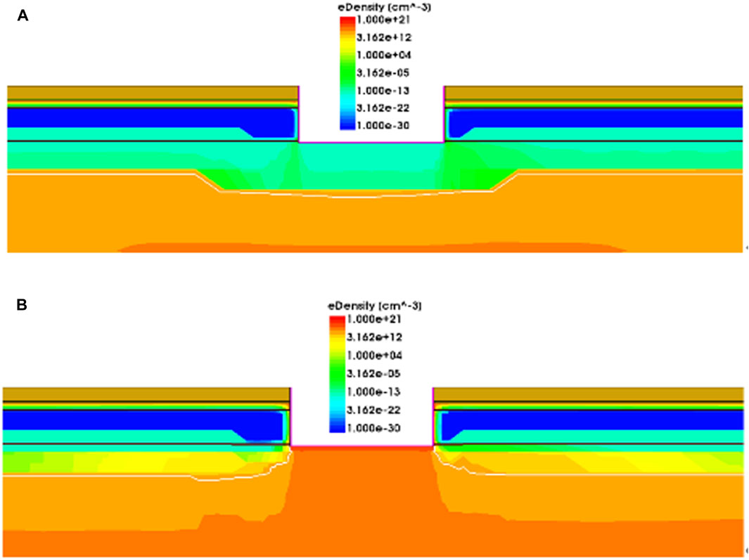
FIGURE 2. Electron concentration distribution (A) off state and (B) on state.
Figure 3 shows the transfer curves (Vds = 1 V) and output curves (Vgs = 5 V) of CONV, SJ-CAVET and LG-SJCAVET, where LG-SJCAVET is the simulated result of the device with unknown parameters of Tp = 9
FIGURE 3. Open-state characteristic curves of CONV, SJ-CAVET and LG-SJCAVET (A) transfer characteristic curve (B) output characteristic curve.
Figure 4 shows the breakdown curves of CONV, SJ-CAVET and LG-SJCAVET. When the voltage applied to the gate is less than the threshold voltage of the device, the device is in the reverse blocking state. Then, a forward voltage is gradually applied to the drain, and the breakdown voltage of the device is defined as the voltage when the drain current reaches 1*10−6A/mm or the peak electric field in the device reaches 4 MV/cm. It can be seen from the breakdown curves that the breakdown voltages of the three devices increase in order under the same conditions. The breakdown voltage of LG-SJCAVET is 2954 V, which is 25.74% higher than that of SJ-CAVET and 55.47% higher than that of CONV.
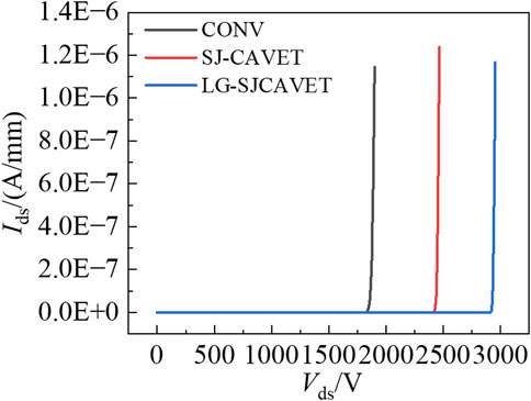
FIGURE 4. Off-state characteristic curves of CONV, SJ-CAVET and LG-SJCAVET.
Combining the simulation results of Figure 3 and Figure 4, we conclude that compared to the SJ-CAVET with the same device structure parameters, the LG-SJCAVET with a gradient AlGaN structure in the buffer layer can significantly increase the breakdown voltage of the device, while the change in the device’s on-resistance is not significant. To evaluate the performance of the devices with different breakdown voltages and on-resistances, we use the figure of merit (FOM) parameter of the power device. By calculating the FOM of the device using Eq. 5 [19], the FOM of the LG-SJCAVET is 5.27
From the above simulation results, it can be seen that the breakdown voltage of the conventional GaN VHFET is 1890 V and its on-resistance is 1.15
To deeply analyze the intrinsic mechanism of achieving high breakdown voltage and low on-resistance in LG-SJCAVET, we compared the current density distribution in the on-state between SJ-CAVET and LG-SJCAVET, as well as the equipotential lines and electric field distribution in the off-state.
The two-dimensional current density distribution of CONV, SJ-CAVET, and LG-SJCAVET are shown in Figure 5A. When the devices are all in the conducting state, only the N-type doping region can conduct current due to the reverse bias state of the N-substrate/P-pillar/junction and N-pillar/p-pillar/junction. The width of the current path in the N-type doping region is reduced due to the depletion region formed by the reverse bias of the PN junction. As can be seen from the distribution maps below, the current in the current path of LG-SJCAVET is slightly lower than that in SJ-CAVET due to the effect of the depletion region of the PN junction and the higher hole concentration caused by the linear gradient AlGaN buffer layer. This causes the current path of LG-SJCAVET to narrow and the saturated drain current to decrease, while also increasing the device’s on-resistance. Figure 5B shows the two-dimensional potential distribution of CONV, SJ-CAVET, and LG-SJCAVET under breakdown voltage. Compared with SJ-CAVET, the equipotential lines density between the N-pillar and P-pillar in LG-SJCAVET is slightly increased, which means that the electric field near the N-pillar and P-pillar will be enhanced. We can estimate the breakdown voltage of each device by the area enclosed by the one-dimensional electric field distribution curve in Figure 6 and the X-axis. Clearly, the enclosed area of LG-SJCAVET is the largest, followed by SJ-CAVET, and then CONV. This conclusion is consistent with the breakdown curves.
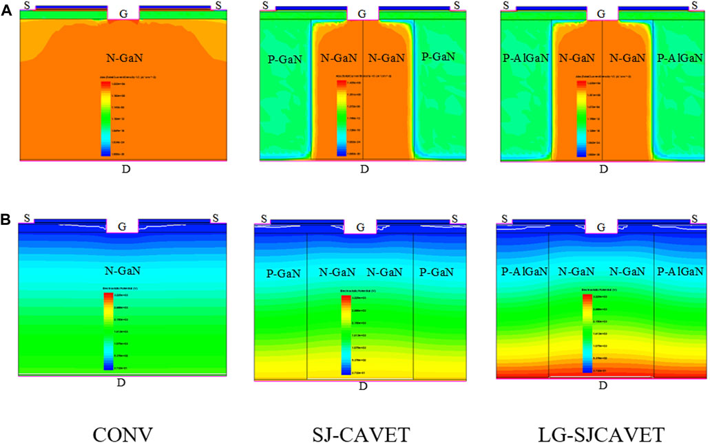
FIGURE 5. (A) Two-dimensional current density distribution and (B) two-dimensional potential distribution at breakdown voltage of CONV, SJ-CAVET and LG-SJCAVET.
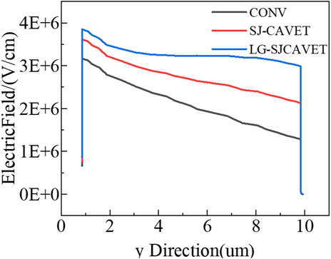
FIGURE 6. One-dimensional electric field distribution along the mn tangent for CONV, SJ-CAVET and LG-SJCAVET at breakdown voltage.
3 Results
3.1 Study of AlGaN buffer layer width
When Tp is 9
The transfer characteristics and output characteristics of LG-SJCAVET as a function of different AlGaN buffer layer widths are shown in Figure 7. From Figure 7A, it can be seen that the threshold voltage of the device remains almost constant with increasing AlGaN buffer layer width, while the saturation drain current decreases with increasing AlGaN buffer layer width. This is because the current path becomes narrower during conduction, leading to a decrease in the saturation drain current. When Wp = 1
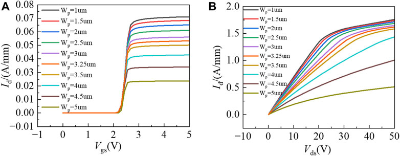
FIGURE 7. Trend of LG-SJCAVET open-state characteristic curves with different AlGaN buffer layer widths (A) Transfer characteristic curve (B) Output characteristic curve.
The trend of breakdown voltage, on-state resistance, and power figure of merit of the LG-SJCAVET with different widths of AlGaN buffer layer is shown in Figure 8. As shown in Figure 8A, both the breakdown voltage and on-state resistance of the device increase with the increasing width of AlGaN buffer layer. This is because in LG-SJCAVET, a larger width of AlGaN buffer layer leads to a narrower width of conductive N-pillar, which narrows the current path during conduction, resulting in a decrease of the saturation drain current and an increase of on-state resistance. The change of on-state resistance shows a trend from gentle to steep. When Wp is 1
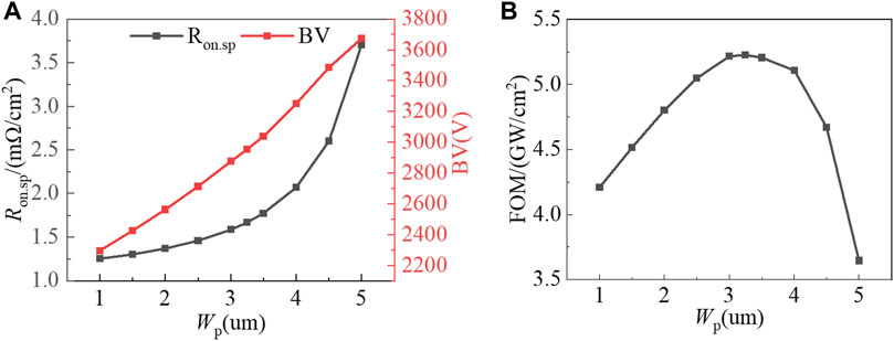
FIGURE 8. Trend of (A) breakdown voltage, on-resistance and (B) power figure of merit of LG-SJCAVET with different AlGaN drift layer widths.
3.2 Study of AlGaN buffer layer components
When Tp is 9
The transfer and output characteristics of the LG-SJCAVET with different maximum Al compositions of the AlGaN buffer layer are shown in Figure 9. As can be seen from Figure 9A, the saturation drain current of the device slightly decreases with the increase of the maximum Al composition of the AlGaN buffer layer. This is because the width of the current path in the device remains almost unchanged during the conduction process, while the total polarization intensity of the AlGaN material increases with the increase of the Al composition, resulting in an increase in the hole concentration generated by the polarization effect, thereby slightly reducing the drain current of the device. When Xp = 0.09, the saturation drain current of the device is 55 mA/mm, and when Xp = 0.81, the saturation drain current of the device is 52 mA/mm. As shown in Figure 9B, under the same gate bias, the slope of the output curve of the device slightly decreases with the increase of the maximum Al composition of the AlGaN buffer layer, while the on-resistance of the device slightly increases with the increase of the maximum Al composition of the AlGaN buffer layer. When Xp = 0.09, the on-resistance of the device is 1.63
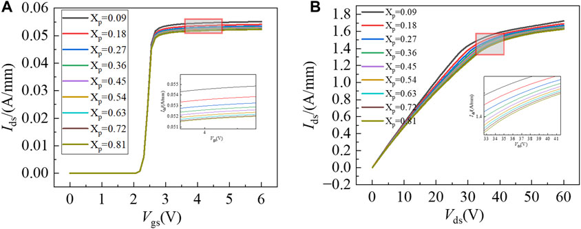
FIGURE 9. Trend of the open-state characteristic curve of LG-SJCAVET with the maximum Al component of different AlGaN drift layers (A) Transfer curve (B) Output curve.
Figure 10 shows the trend of breakdown voltage, on-resistance, and figure of merit (FOM) of the LG-SJCAVET with different maximum Al compositions in the AlGaN buffer layer. As shown in Figure 10A, the breakdown voltage of the device increases significantly with increasing Xp, and the on-resistance presents a slightly increasing trend with a gentle slope. When Xp is 0.09, the device has a breakdown voltage of 2600V, while it reaches 3971 V when Xp is 0.81. As Xp increases, the breakdown voltage of the device improves due to the higher voltage resistance of the buffer layer. The graded Al composition of the AlGaN buffer layer helps to distribute the electric field more uniformly. As shown in Figure 10B, the FOM of the device increases with the maximum Al composition of the AlGaN buffer layer. According to the definition of FOM, the device exhibits the best power performance when Xp is 0.81, with a breakdown voltage of 3971 V, which is significantly higher than that of CONV and SJ-CAVET. However, it is difficult to fabricate AlGaN materials with an Al composition greater than 0.8 in current engineering practice. Therefore, considering the simulation results and fabrication requirements, Xp = 0.72 is the optimal choice [22, 23].
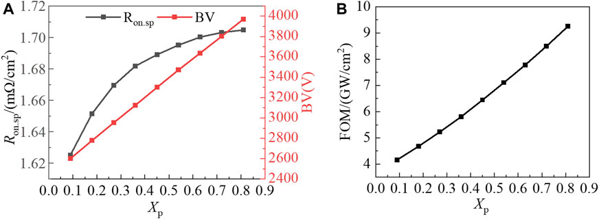
FIGURE 10. Trend of (A) breakdown voltage, on-resistance and (B) power figure of merit of LG-SJCAVET with different AlGaN drift layer maximum Al components.
Figure 11 gives a comparative analysis of the simulation results of this paper with domestic and international research works, and it can be seen from the figure that the new device structure designed in this paper exhibits good on-state and breakdown characteristics compared to devices of the same type [24–28], and at the same time is closer to the physical limit value of GaN material, and the device has a larger power figure of merit.
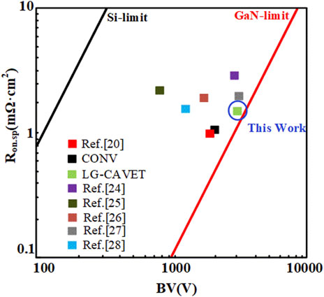
FIGURE 11. Comparison between devices in the related literature and the simulation results of this paper BV, Ron. sp.
4 Discussion
In this paper, the LG-SJCAVET structure is proposed, characterized by the use of polarization-doped AlGaN material instead of the traditional P-type GaN buried layer, and the use of the linear gradient of the AlGaN material can generate hole gas inside this feature, to achieve the P-type doping, and the material inside the hole gas concentration is large, good thermal stability. The operating principle of the device is analyzed, the structural parameters of the device are optimized, and the contradiction between high breakdown voltage and low on-resistance of the device is effectively solved, and the simulation results and laws with certain reference value are obtained. However, the results of this paper are based on numerical simulations, and the actual power characteristics of the device need to be further confirmed since they are not actually verified by flowing.
Data availability statement
The original contributions presented in the study are included in the article/Supplementary Material, further inquiries can be directed to the corresponding author.
Author contributions
YC conceived the project. YC and YY drafting and refining the manuscript. JZ and YS critical reading of the manuscript. All authors contributed to the article and approved the submitted version.
Funding
This work was supported by National Natural Science Foundation of China (No. 62041403), Guangxi Key Laboratory of Precision Navigation Technology and Application (No. DH201510), Guangxi Key Laboratory of Wireless Wideband Communication and Signal Processing (No. GXKL06200119).
Acknowledgments
The authors are grateful to the editors and referees for their valuable suggestions and comments, which greatly improved the presentation of this article.
Conflict of interest
The authors declare that the research was conducted in the absence of any commercial or financial relationships that could be construed as a potential conflict of interest.
Publisher’s note
All claims expressed in this article are solely those of the authors and do not necessarily represent those of their affiliated organizations, or those of the publisher, the editors and the reviewers. Any product that may be evaluated in this article, or claim that may be made by its manufacturer, is not guaranteed or endorsed by the publisher.
Supplementary material
The Supplementary Material for this article can be found online at: https://www.frontiersin.org/articles/10.3389/fphy.2023.1176519/full#supplementary-material
References
1. Wang M, Chen KJ. Off-state breakdown characterization in algan/Gan hemt using drain injection technique. IEEE Trans Electron Devices (2010) 57(7):1492–6. doi:10.1109/TED.2010.2048960
2. Baliga BJ. Power semiconductor device figure of merit for high-frequency applications. IEEE Electron Device Lett (1989) 10(10):455–7. doi:10.1109/55.43098
3. Jiang Q, Liu C, Chen Y, Chen KJ. 1.4-Kv algan/Gan hemts on a Gan-on-Soi platform. IEEE Electron Device Lett (2013) 34(3):357–9. doi:10.1109/led.2012.2236637
4. Dong Z, Tan S, Yong C, Chen H, Liu S, Xu J, et al. 5.3a/400v normally-off algan/Gan-on-Si mos-hemt with high threshold voltage and large gate swing. Electro Lett (2013) 49(3):221–2. doi:10.1049/el.2012.3153
5. Rongming C, Corrion A, Chen M, Ray L, Wong D, Zehnder D, et al. 1200-V normally off Gan-on-Si field-effect transistors with low dynamic on -resistance. Electron Device Letters, IEEE (2011) 32(5):632–4. doi:10.1109/led.2011.2118190
6. Medjdoub F, Zegaoui M, Grimbert B, Ducatteau D, Rolland N, Rolland PA. First demonstration of high-power Gan-on-Silicon transistors at 40 ghz. Electron Device Lett IEEE (2012) 33(8):1168–70. doi:10.1109/led.2012.2198192
7. Ben-Yaacov I, Seck YK, Heikman S, Denbaars SP, Mishra UK. Algan/Gan current aperture vertical electron transistors. In: Proceedings of the Drc Conference Digest Device Research Conference; June 2002; Santa Barbara, CA, USA (2002).
8. Ben-Yaacov I, Seck YK, Mishra UK, DenBaars SP. Algan/Gan current aperture vertical electron transistors with regrown channels. J Appl Phys (2004) 95(4):2073–8. doi:10.1063/1.1641520
10. Zhongda L, Chow T. Paul. Design and simulation of 5–20-kv Gan enhancement-mode vertical superjunction hemt. IEEE Trans Electron Devices (2013) 60(10):3230–7. doi:10.1109/TED.2013.2266544
11. Jiangfeng D, Zhao Z, Zhiyuan L, Bai Z, Li L, Mo J, et al. Design of high breakdown voltage Gan vertical hfets with P-Gan buried buffer layers for power switching applications. Superlattices and Microstructures (2015) 83:251–60. doi:10.1016/j.spmi.2015.03.039
12. Ji D, Laurent MA, Agarwal A, Li W, Mandal S, Keller S, et al. Normally off trench cavet with active Mg-doped Gan as current blocking layer. IEEE Trans Electron Devices (2017) 64(3):805–8. doi:10.1109/TED.2016.2632150
13. Shelton BS, Huang JJ, Lambert D, Zhu TG, Wong MM, Eiting CJ, et al. Algan/Gan heterojunction bipolar transistors grown by metal organic chemical vapour deposition. Electro Lett (2000) 36(1):80–1. doi:10.1049/el:20000053
14. Kozodoy P, Xing H, DenBaars SP, Mishra UK, Saxler A, Perrin R, et al. Heavy doping effects in Mg-doped Gan. J Appl Phys (2000) 87(4):1832–5. doi:10.1063/1.372098
15. Shenoy PM, Bhalla A, Dolny GM. Analysis of the effect of charge imbalance on the static and dynamic characteristics of the super junction mosfet. In: Proceedings of the 11th International Symposium on Power Semiconductor Devices and ICs. ISPSD'99 Proceedings (Cat. No.99CH36312); May 1999; Toronto, ON, Canada (1999).
16. Simon J, Protasenko V, Lian C, Xing H, Jena D. Polarization-induced hole doping in wide-band-gap uniaxial semiconductor heterostructures. Science (2010) 327:60–4. doi:10.1126/science.1183226
17. Zhang L, Ding K, Yan JC, Wang JX, Zeng YP, Wei TB, et al. Three-dimensional hole gas induced by polarization in (0001)-oriented metal-face iii-nitride structure. Appl Phys Lett (2010) 97(6):252105. doi:10.1063/1.3478556
18. Khan MA, Bhattarai A, Kuznia JN, Olson DT. High electron mobility transistor based on a GaN/AlxGa1−xN heterojunction. Appl Phys Lett (1993) 63(9):1214–5. doi:10.1063/1.109775
19. Saito W, Takada Y, Kuraguchi M, Tsuda K, Omura I, Ogura T, et al. High breakdown voltage AlGaN/GaN power-HEMT design and high current density switching behavior. IEEE Trans Electron Devices (2003) 50(12):2528–31. doi:10.1109/ted.2003.819248
20. Bernardini F, Fiorentini V, Vanderbilt D. Spontaneous polarization and piezoelectric constants of iii-V nitrides. Physrevb (1997) 56(16):10024–7. doi:10.1103/physrevb.56.r10024
21. Shibata D, Kajitani R, Ogawa M, Tanaka K, Tamura S, Hatsuda T 1.7 kV/1.0 mΩ·cm2 normally-off vertical GaN transistor on GaN substrate with regrown p-GaN/AlGaN/GaN semipolar gate structure. In: Proceedings of the 2016 IEEE International Electron Devices Meeting (IEDM); December 2016; San Francisco, CA, USA. IEEE (2016).
22. Li W, Zhu M, Nomoto K, Hu Z, Gao X, Pilla M, et al. Enhancement of punch-through voltage in Gan with buried P-type layer utilizing polarization-induced doping. In: Proceedings of the 2018 IEEE 30th International Symposium on Power Semiconductor Devices and ICs (ISPSD); May 2018; Chicago, IL, USA (2018).
23. Santi CD, Fabris E, Nomoto K, Hu Z, Li W, Gao X, et al. Demonstration of avalanche capability in polarization-doped vertical Gan pn diodes: study of walkout due to residual carbon concentration. In: Proceedings of the 2018 IEEE International Electron Devices Meeting (IEDM); December 2018; San Francisco, CA, USA (2018).
24. Du J, Liu D, Zhao Z, Bai Z, Li L, Mo J, et al. Design of high breakdown voltage GaN vertical HFETs with p-GaN buried buffer layers for power switching applications. Superlattices & Microstructures (2015) 83:251–60. doi:10.1016/j.spmi.2015.03.039
25. Ji D, Agarwal A, Li H, Li W, Keller S, Chowdhury S. 880V/2.7mΩ·cm2 MIS gate trench CAVET on bulk GaN substrates. IEEE Electron Device Lett (2018) 39:863–5. doi:10.1109/led.2018.2828844
26. Hui N, Diduck Q, Alvarez B, Edwards AP, Kayes BM, Zhang M 1.5-kV and 2.2-mΩ-cm2 vertical GaN transistors on bulk-GaN substrates. IEEE Electron Device Lett (2014) 35(9):939–41. doi:10.1109/LED.2014.2339197
27. Du J, Liu D, Bai Z, Liu Y, Yu Q. Design of high breakdown voltage GaN-based vertical HFETs with p-GaN island structure for power applications. Superlattices and Microstructures (2015) 85:690–6. doi:10.1016/j.spmi.2015.06.043
Keywords: vertical GaN-based power devices, super-junction, AlGaN polarization effect, breakdown voltage and specific on-resistance, power figure of merit
Citation: Chen Y, Yang Y, Zhai J and Sun Y (2023) Research on vertical GaN devices based on gradient Al components. Front. Phys. 11:1176519. doi: 10.3389/fphy.2023.1176519
Received: 28 February 2023; Accepted: 19 October 2023;
Published: 02 November 2023.
Edited by:
Mauro Guerra, New University of Lisbon, PortugalReviewed by:
Binghui Li, Chinese Academy of Sciences (CAS), ChinaMarco Mandurrino, National Institute of Nuclear Physics of Turin, Italy
Copyright © 2023 Chen, Yang, Zhai and Sun. This is an open-access article distributed under the terms of the Creative Commons Attribution License (CC BY). The use, distribution or reproduction in other forums is permitted, provided the original author(s) and the copyright owner(s) are credited and that the original publication in this journal is cited, in accordance with accepted academic practice. No use, distribution or reproduction is permitted which does not comply with these terms.
*Correspondence: Jianghui Zhai, 39808723@qq.com