Optical and electronic signal stabilization of plasmonic fiber optic gate electrodes: towards improved real-time dual-mode biosensing
 Roger Hasler1,2*
  Marie-Helene Steger-Polt2
  Ciril Reiner-Rozman2 Stefan Fossati1 Seungho Lee3 Patrik Aspermair1,2
  Christoph Kleber2
  Maria Ibáñez3
  Jakub Dostalek1,2,4
  Wolfgang Knoll1,2*
- 1AIT Austrian Institute of Technology GmbH, Tulln, Austria
- 2Laboratory for Life Sciences and Technology (LiST), Faculty of Medicine and Dentistry, Danube Private University, Krems, Austria
- 3Institute of Science and Technology Austria (ISTA), Klosterneuburg, Austria
- 4FZU-Institute of Physics, Czech Academy of Sciences, Prague, Czech Republic
The use of multimodal readout mechanisms next to label-free real-time monitoring of biomolecular interactions can provide valuable insight into surface-based reaction mechanisms. To this end, the combination of an electrolyte-gated field-effect transistor (EG-FET) with a fiber optic-coupled surface plasmon resonance (FO-SPR) probe serving as gate electrode has been investigated to deconvolute surface mass and charge density variations associated to surface reactions. However, applying an electrochemical potential on such gold-coated FO-SPR gate electrodes can induce gradual morphological changes of the thin gold film, leading to an irreversible blue-shift of the SPR wavelength and a substantial signal drift. We show that mild annealing leads to optical and electronic signal stabilization (20-fold lower signal drift than as-sputtered fiber optic gates) and improved overall analytical performance characteristics. The thermal treatment prevents morphological changes of the thin gold-film occurring during operation, hence providing reliable and stable data immediately upon gate voltage application. Thus, the readout output of both transducing principles, the optical FO-SPR and electronic EG-FET, stays constant throughout the whole sensing time-window and the long-term effect of thermal treatment is also improved, providing stable signals even after 1 year of storage. Annealing should therefore be considered a necessary modification for applying fiber optic gate electrodes in real-time multimodal investigations of surface reactions at the solid-liquid interface.
1 Introduction
Label-free biomolecular interaction analysis is of increasing importance in numerous fields of life sciences research, development of bioanalytical technologies and investigation of functional biointerfaces. It provides attractive means to directly observe interactions between biomolecular species and their affinity partners in real-time without the need of conjugation with markers. Several transducer principles have been introduced, among which surface plasmon resonance (SPR) biosensors [1] represent an established technology and electrolyte-gated field effect transistors (EG-FET) [2] are rapidly progressing in this field. The information obtained from such surface-sensitive techniques is particularly useful for real-time monitoring of affinity binding events [3–6] and involved biomolecule conformational changes [7, 8] at surfaces. More recently, parallel SPR and EG-FET analysis was reported and demonstrated that the time dependent electrical FET response can be directly correlated with mass adsorption [9]. Furthermore, it has been shown that such parallel dual monitoring of surface reactions in real-time, using a combination of SPR on the gate electrode of an EG-FET, provides new insights into complex processes occurring at the solid-liquid interface that are beyond the reach of the individual techniques [10]. The simultaneous real-time measurements allowed elucidating the effects of surface charge and mass adsorption and redistribution during the growth of differently charged polyelectrolyte multilayers. Typically, such effects would be inaccessible if measured by an endpoint readout with conventional implementations of SPR/FET. Along these lines, we recently developed a further modification of such a SPR/FET combined platform based on fiber optic (FO) SPR [11]. FO SPR sensors are easy to fabricate and have shown great potential for real-life applications, such as the detection of heavy metal ions in drinking water [12]. In combination with a FET the gold-coated FO tip allows for probing with a confined surface plasmon electromagnetic field the interface that simultaneously act as the gate electrode for the FET, yielding a miniaturized and portable multimodal sensor system.
A fundamental question that needs to be addressed when combining different transducing principles is how the combination thereof influences the individual signals. Since combining SPR with electrochemical methods, it has been clear that an applied electrochemical potential affects the plasmon resonances. It has been reported that metal films can undergo potential-induced crystal grain growth, leading to an irreversible blue-shift of the plasmon resonance [13]. Furthermore, applying an electrochemical potential influences the chemical equilibrium of the reversible ionic complex adsorption on the metal surface, mainly dominating the potential-induced plasmonic response [14].
On the other hand, morphological changes in the metal, e.g., gold, film can be induced by annealing [15, 16], allowing the formation of metallic islands which results in an enhanced plasmonic response [17]. This effect has been used to increase the sensitivity of FO-SPR tips for improved plasmonic biosensing [18]. Alternatively, gold surface morphological changes on FO substrates can also be induced by exposure to a harsh chemical medium [19]. Certainly, such changes in the electrode surface morphology are also expected to affect the electric double-layer capacitor and therefore influence not only the optical but also the electronic response [20]. Therefore, it is essential to understand how these material properties affect the overall device performance, especially for prolonged potential application when the device is operated for real-time sensing. Furthermore, such effects are expected to affect the signal stability of both transducing principles when used in combination. High signal stability is of great importance for the simultaneous real-time analysis of affinity binding interactions at the solid-liquid interface using the developed platform. Thus, it is crucial to identify the impact of the transducers’ surface morphology and the potential- or thermal-induced tunability thereof.
Hence, in this work, we investigate the influence of gold FO-SPR gate surface morphology changes induced by annealing on the resulting optical and electronic response. We discuss the impact thereof on the device performance factors and show that a thermal treatment of the FO-SPR gate after its coating with a thin gold film, provides a more reliable readout over an extended measurement time window. We show that the thermal exposure of the FO-SPR gate leads to superior optical and electronic signal stabilization when applied for its dual-mode purpose. This provides an alternative strategy to surface passivation with, e.g., a thiol self-assembled monolayer (SAM) typically utilized in FO-SPR/FET biosensors when applied for the probing of assays on their surface. Furthermore, thermally induced optical and electronic signal stability persists even after 1 year of storage, ensuring a prolonged shelf-life of FO-SPR gate electrodes without changes in their performance.
2 Materials and methods
(3-Aminopropyl)triethoxysilane (APTES, 99%), potassium chloride (≥99%), hydrazine monohydrate (64%–65%, reagent grade 98%) were purchased from Sigma Aldrich. Phosphate Buffered Saline (PBS) tablets, ethanol (absolute, 99.8%), and isopropanol were purchased from VWR. Graphene oxide (GO) water dispersion (0.4 wt%) was obtained from Graphenea. Alkane thiols, containing oligo ethylene glycol (OEG) units, with a terminal carboxyl group (thiol-OEG-COOH, HS-C11-EG6-OCH2-COOH) and hydroxyl group (thiol-OEG-OH, HS-C11-EG6) were obtained from ProChimia Surfaces. All chemicals were used as received without further purification.
FO-SPR gate electrodes were prepared according to a previously reported procedure [11]. Briefly, FO tips with a total length of 6.5 cm were prepared from TECS-clad step-index multimode optical fiber cable (Thorlabs Inc.) with a core diameter of 1 mm. At one end of the tip a 1 cm long SPR-active zone was constructed by removing the jacket layer with a dedicated stripping tool and the cladding layer by dissolution in acetone. To obtain a planar cut at the end face of the SPR-active zone a fiber scribe with a ruby blade was used. FO tips were cleaned with Milli-Q grade DI-H2O, followed by isopropanol, and blow dried with compressed air. The tips were coated with 50 nm of gold in an EM ACE600 sputter coater (Leica Microsystems) using a sputter rate of 0.11 nm/s. A rotational stage was used, allowing sample rotation around two axes, to ensure a homogenous coating of the FO tips.
As prepared tips where then either used directly without further temperature annealing (designated as “RT” = room temperature) or with a mild thermal annealing of the as-sputtered gold surface. Therefore, the tips were exposed to a temperature treatment in an oven (Heraeus T12) at 130, 180, and 230°C in a time range of 2, 7, or 12 h, according to a previously reported method [18]. Alternatively, on tips without thermal annealing a thiol SAM was formed by exposing them overnight to a 1 mM solution in ethanol of thiol-OEG-COOH/thiol-OEG-OH (molar ratio 1:4) (denoted as “COOH-OEG SAM”). As previously described, all tips were further modified with a layer of conductive silver paint (RS Components Ltd.) and a coating with liquid insulation tape (Performix Liquid Tape, Plastidip®, Plasti Dip Europe GmbH) to ensure a sufficient electrical connection across the transition to the optically and electrically active part of the FO-SPR gate electrode [11]. As-prepared FO-SPR gate electrodes were stored in argon until further usage. The surface morphology was characterized using Scanning Electron Microscopy (SEM) (Zeiss SUPRATM 40 Field Emission Scanning Electron Microscope).
FETs were fabricated using a previously described procedure [21]. Briefly, commercially available substrates with interdigitated source-drain electrodes (channel width 10 μm, channel length 490 mm, MicruX Technologies) were pre-functionalized by immersion in a 1% APTES-solution in ethanol and subsequently GO (0.019 wt%, in Milli-Q grade DI-H2O) was spin coated (1800 rpm, 60s) over their surface. The obtained GO-coated substrates were chemically reduced in hydrazine vapor at 80°C followed by annealing at 200°C for 2 h.
FO-SPR gate electrodes were connected simultaneously to an optical and electronic setup as previously described [11]. Briefly, FO-SPR gate electrodes were inserted into a bare fiber terminator (Thorlabs Inc.), modified with conductive copper tape (Reichelt Elektronik GmbH and Co. KG) to ensure an electrical contact for the use as gate electrode. Polychromatic light from a halogen light source (12 V, HL-2000-LL, Ocean Insight) was launched into the input arm of a Y-optical splitter and guided to the tip. The light back reflected at the tip was collected to the output arm of the Y-optical splitter connected to a spectrometer (HR4000, Ocean Insight). The acquired spectrum was normalized with that of the FO-SPR gate in air. Optically connected fiber tips were used simultaneously as gate electrode in an EG-FET configuration (Figure 1A). Therefore, the FO-SPR gate was dipped into a reaction chamber containing the electrolyte solution. At the bottom of the chamber the FET substrate was inserted and connected to a Keithley 4200-SCS probe station. For all experiments, a drain-source voltage of 50 mV was applied.
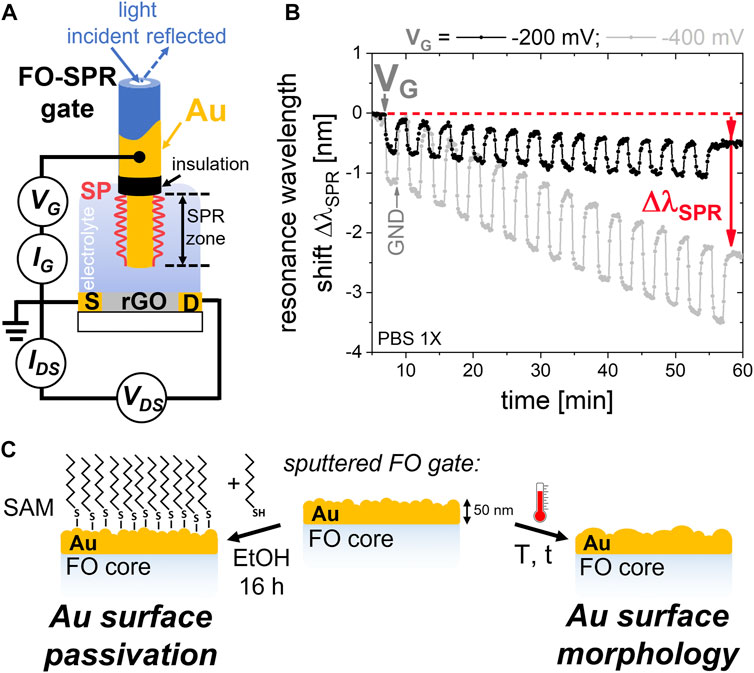
FIGURE 1. (A) Schematic representation of the FO-SPR/FET platform. (B) Resonance wavelength shift obtained upon cycling the gate potential Vg between OFF (“GND” = ground) and −200 mV or −400 mV. Red arrows indicate the overall blue-shift. (C) Possible strategies for FO-SPR gate stabilization via gold surface passivation with a SAM or thermal treatment influencing the gold surface morphology.
3 Results and discussion
3.1 Dual-mode operation of the FO-SPR/FET setup
The gold-coated part of the FO-SPR gate electrode is electrically contacted with the SPR active zone and immersed into the electrolyte solution on the top of the FET substrate, as illustrated in Figure 1A. A gate voltage is applied, and the resulting drain-source current modulation can be described in the linear region of EG-FET devices,
where
3.2 Thermal annealing: impact on the optical signal characteristics
As-sputtered FO-SPR gates were therefore thermally annealed at 130, 180, and 230°C for 2, 7, and 12 h. This range of investigated temperatures has been previously reported to induce structural changes in the thin gold layer without damaging the other layers of the fiber optic probe, leaving the possibility for optical sensing intact [18]. Figure 2A shows the SEM images of the FO-SPR gate surface after sputtering and after annealing at 180°C for 7 h, respectively. After sputtering, the gold surface shows a pronounced granular morphology. The thermal treatment leads to a coalescence of the Au grains into larger domains. This agrees with a previously reported study that shows that this temperature and time range does not lead to a significant change of the surface roughness but rather a strong increase of the average grain size lateral dimension [18]. Similar effects on increasing the grains lateral dimension upon annealing have been reported using scanning tunneling microscopy (STM) [15]. The observed grain growth depends on the strength and time duration of the applied temperature increase. At elevated temperatures, thin, continuous gold films are known to form island-like structures with voids [26]. It has been reported that surface diffusion dominates the thermal annealing process of thin gold films with a relatively low thermal activation energy [15, 25, 27, 28]. As a result, the optical signal shows a significant blue-shift of ΔλSPR = −52.3 ± 1.2 nm (Figure 2B and Supplementary Figure S1) and, furthermore, a significant reduction in full width half maximum (FWHM) of the plasmonic dip (Supplementary Figure S1) of ΔFWHM = −25.7 ± 4.9 nm, compared to the signal of the FO-SPR gate after sputtering without thermal treatment (denoted as “RT”). This further indicates that the dominating effect is not an increase in surface roughness since an increased surface roughness would lead to a broadening of the SPR dip in the reflectivity spectrum [29, 30] due to the more pronounced damping of surface plasmons [29, 31]. More importantly, the FWHM impacts the optical signal’s spectral resolution and is, therefore, an important measure of the quality of the FO-SPR gate. Mild thermal annealing not just shifts the resonance dip to lower wavelengths which opens a larger measurement window but also leads to a narrowing of the resonance dip, improving the overall resolution.
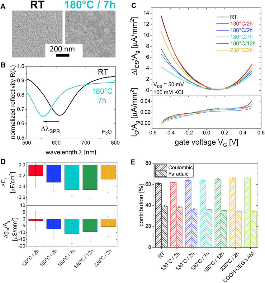
FIGURE 2. (A) Representative SEM images of the FO-SPR gate after sputtering and after thermal treatment at 180°C for 7 h, and (B) corresponding SPR spectrum obtained before and after thermal exposure. (C) IDSVG transfer curves and leakage current (IG) for differently annealed FO-SPR gate electrodes, normalized by the gate surface area Ag. (D) Change in total interfacial capacitance and maximum transconductance for different annealing conditions. (E) Deconvolution of Coulombic and Faradaic contributions for different annealing conditions or surface passivation with a COOH-OEG SAM.
It has to be noted that the annealing step also impacts the bulk refractive index sensitivity SB of the FO-SPR gate. In a previously reported study a significant increase in bulk sensitivity was observed after annealing the FO tips in the investigated temperature range [18]. The authors of this study associate this sensitivity improvement with an increased plasmonic behavior at the semi-continuous domains created due to the thermal treatment. We have not observed such a sensitivity increase but rather a decrease, associated with the spectral blue-shift of the resonance wavelength. It has been shown with ellipsometry that various annealing temperatures below 300°C cause changes of the (effective) optical constants of gold films deposited on silicon substrates [32]. This results in a change of the resonance condition and a blue-shift of the resonance wavelength. The determined SB after the thermal annealing is in accordance with the analytical model based on Fresnel multilayer reflectivity that suggests SB decreasing when decreasing the SPR wavelength (Supplementary Figure S2). However, even the reduced SB provides a high enough sensitivity for the intended application of the FO-SPR gate for multimodal biosensing and is not the only parameter to consider when discussing the overall quality of the optical signal. As shown in Supplementary Figure S3, the spectral quality (Q-factor) as well as the refractive index resolution is improved for all annealing conditions compared to as-sputtered FO-SPR gate electrodes.
3.3 Thermal annealing: impact on the electronic signal characteristics
To evaluate the impact of the surface morphology change due to thermal annealing on the electronic sensing, such FO-SPR gates were connected in an EG-FET configuration using FETs with reduced graphene oxide (rGO) as channel material. The FO-SPR gates were then immersed in the reaction chamber containing 100 mM KCl as electrolyte and the FET substrate at the bottom (Figure 1A). IDSVG transfer curves for different annealing conditions were recorded, with a VDS of 50 mV, using the same FET substrate immersed in the electrolyte and exchanging the FO-SPR gate consecutively. For rGO, typical ambipolar transfer curves were obtained, with the minimum being denoted as Dirac point Vi. The recorded curves have been aligned by subtracting the minimum current at the Dirac point IDS(Vi), therefore plotting the drain-source current shift ΔIDS = IDS(VG)—IDS(Vi), to eliminate a possible signal drift. As previously reported, the electronic signal obtained from this FO-SPR gate electrodes strongly depends on the FO-SPR gate surface area Ag [11]. The obtained drain-source current shifts were normalized by the geometrical surface area Ag for the given FO-SPR gate (average Ag: 29 ± 2 mm2) to avoid the influence thereof due to differences in length for the differently annealed fiber tips. Obtained results for the transfer curve and the leakage current IG are shown in Figure 2C. The surface morphology change of the FO-SPR gate causes a significant impact on the gate-electrolyte interfacial capacitance and therefore affects the slope of the hole and electron accumulation branch, respectively.
The microscopic changes of the FO-SPR gate surface affect the electronically active surface area A and, thus, the formation of the electrical double layer. The associated change in capacitance can be related to a change in surface area by the well-known capacitor equation
As previously described [11], by recording the leakage current at different scan rates while sweeping VG, it is possible to deconvolute Coulombic and Faradaic contributions. Untreated FO-SPR gate electrodes show an increase in Faradaic currents as a result of increasing the geometrical FO-SPR gate area by using a larger fiber core diameter [11]. Potential Faradaic side reactions occurring during EG-FET operation might form reactive side products that could harm the devices’ biological functionalization or lead to accelerated degradation [35]. Interestingly, upon thermal annealing, the Faradaic contribution can be reduced, possibly overcoming this drawback to some extent (Figure 2E). A table summarizing the optical and electronic performance factors obtained after the different thermal treatments can be found in the SI (Supplementary Table S1).
Alternatively, the FO-SPR gate can be passivated using a standard carboxy-terminated thiol SAM. It has been reported that applying a thiol SAM on the gate in a top-gated EG-FET configuration leads to a decrease in capacitance [36]. This results in shallower slopes and reduced transconductance for SAM-coated FO-SPR gates (data not shown). However, the terminal end groups of the SAM molecules provide possible anchor points for surface functionalization typically used in bioassays. Similar to the shallower transfer curves of thermally annealed FO-SPR gates, the electronic performance is still deemed to be sufficient for sensing applications. Moreover, as expected, the gate surface passivation with a SAM reduces the Faradaic contributions to a minimum (Figure 2E).
3.4 Dual-mode signal stabilization
To investigate the possible effect on optical signal stabilization, FO-SPR gate electrodes were connected optically and electronically with and without annealing. The optical signal was recorded by tracking the resonance wavelength λSPR over time and a gate potential of VG = −500 mV was applied in pulses of 30 s. Pulses were applied by switching VG ON and OFF (GND) and the drain-source current was recorded at a constant drain-source voltage for a period of 1 h. The simultaneously obtained optical and electronic signals are shown in Figures 3A, B. As can be seen in these data the potential cycles significantly impact the optical signal and a strong blue-shift of the SPR wavelength is observed for as-prepared FO-SPR gate electrodes over the period of 1 h. After the potential cycling is terminated, the resonance wavelength stays shifted, illustrating the irreversibility of this effect. A mild thermal treatment of 130°C for 2 h does not lead to a significant improvement. In both cases, an irreversible blue-shift of approximately −3 nm was measured (Supplementary Figure S4C). However, all other thermal treatments led to superior optical signal stability, showing no significant signal drift and irreversible blue-shift of the resonance wavelength (Figure 3A). We assume that the thermal stress saturates the surface morphology changes that otherwise would be gradually imposed by applying an electrochemical potential. Interestingly, the current signal also shows improved stability compared to the untreated FO-SPR gate electrode (Figure 3B). Especially in the first 20 min of applying VG cycles, a significant drift of the ON current was observed. In contrast, for a FO-SPR gate exposed to 180°C for 2 h, the ON current levels off and a significant variation is observed only in the first 3 cycles. A pertinent attribute of the transistor is the ION/IOFF ratio. As illustrated in Figure 3B, without thermal annealing, a significant variation of the ION/IOFF ratio was obtained whereas with a thermally treated FO-SPR gate a constant ION/IOFF ratio was observed. This is expected as the same surface morphology changes that affect the optical signal also influence the gate-electrolyte interfacial capacitance, as discussed above. The morphological changes induced by the applied gate potential lead to a decrease of the interfacial capacitance, resulting in lower ION over time. The prior annealing of the FO-SPR gate saturates such changes, as shown in Figure 2D, ensuring a constant ION/IOFF ratio over time.
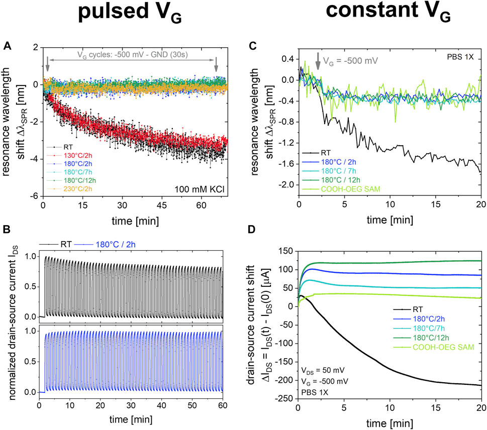
FIGURE 3. Simultaneous real-time measurements of the resonance wavelength shift (A,C) and the drain-source current (B,D) obtained for a pulsed (left) or constant (right) application of VG. A VDS of 50 mV was applied and the signal stability was evaluated using a VG of −500 mV.
Counterions from the electrolyte, e.g., halides, can strongly bind to the surface of the gold electrode [37] and experience high local field strengths upon applying an electrochemical potential [38, 39]. Previous studies suggest that the potential-induced grain growth is related to a gold surface reconstruction induced by counterion adsorption [13]. It has been shown that double-layer charging can cause morphology changes and affects the crystallinity of small gold rods [40]. Therefore, the grain boundaries are expected to act as electrochemical cells, at which atomic reconstruction occurs spontaneously due to reversible interactions with counterions, promoted by the applied potential [13]. The thermal treatment implies a tension on the thin Au layer of the FO-SPR gate and induces grain growth leading to a reduction of grain boundaries compared to the granular surface morphology obtained after sputtering. We hypothesize that this accounts for preventing a further influence of an applied electrochemical potential, leading to the observed optical and electronic signal stabilization. Supplementary Figure S4 shows the obtained spectra before and after 1 h of VG cycles for an untreated and a thermally annealed (180°C/7 h) FO-SPR gate electrode. It is worth noting that the thermally treated FO-SPR gate shows no significant change in the obtained spectrum after the potential cycles. Untreated FO-SPR gates, on the other hand, show a significant blue-shift as already seen for the real-time optical signal. Furthermore, a significant increase in FWHM was also observed (Supplementary Figure S4D). This could be associated with plasmonic damping due to potential-induced changes of the surface morphology. Thermal annealing not just prevents a spectral blue-shift but also the spectral broadening of the resonance dip is eliminated, ensuring a constant optical resolution throughout a dual-mode assay.
High signal stability is of great importance for the real-time dual-mode operation of the FO-SPR/FET platform. In this mode of operation, a constant VG is applied to the FO-SPR gate. As for pulsed VG application, a constant VG of −500 mV also results in a significant signal drift for both the optical and the electronic signal of untreated FO-SPR gate electrodes (Figures 3C, D). This must be carefully considered and corrected when performing adsorption processes on the FO-SPR gate gold surface. As shown in Figure 3C, thermal annealing of the FO-SPR gate leads to superior optical signal stability during VG application. Upon applying a gate voltage, an abrupt decrease of the resonance wavelength is observed. As previously reported, this offset is reversible and is linearly dependent on the applied gate voltage [11]. Only a minor offset of the resonance wavelength of approximately −0.4 nm was observed, possibly due to the change of the equilibrium for ionic complex formation on the surface [14]. For an as-prepared FO-SPR gate this is superimposed with an irreversible blue-shift and therefore a continuous decrease of the resonance wavelength. Thermal annealing prevents the irreversible blue-shift and thus ensures a constant offset of the resonance wavelength upon applying a gate voltage. This is an important characteristic when the FO-SPR gate is operated in its dual-mode purpose. More importantly, also superior stability of the electronic signal was observed due to the thermal pretreatment of the FO-SPR gates (Figure 3D). The measured drain-source current stabilizes within the first 5 min and stays constant, whereas untreated FO-SPR gates showed a continuous decrease in drain-source current, with drift saturation after approximately 20 min. Considering an initial stabilization period of 10 min, an optical signal drift (ΔλSPR/SB)/t, of −0.019 mRIU/min and an electronic signal drift (ΔIDS/IDS (t = 0))/t, of −0.3%/min remains for an as-sputtered FO-SPR gate, evaluated at VG = −500 mV. Thermal exposure of the FO-SPR gate to 180°C for 7 h prior to the measurement yields an improvement of the signal drift by over an order of magnitude, namely, to −0.001 mRIU/min and −0.01%/min for the optical and electronic signal, respectively. The optical signal drift upon prolonged gate-voltage application can be attributed to surface recrystallization of the Au film [13]. The propagation constant of the surface plasmon at a metal-dielectric interface is tightly related to the optical constant of the metal film [1]. Thus, surface morphology changes alter the resonance condition and lead to a shift of the resonance wavelength. The electronic signal on the other hand is tightly related to the interfacial capacitance (Eq. 1). The surface morphology changes induced by the prolonged application of the gate-voltage affect the interfacial area and therefore its capacitance which results in a change of the measured drain-source current. Thermal treatment of the as-sputtered Au film saturates such surface morphology changes and results in Au films that are less affected by the applied gate voltage. Thermal annealing therefore leads simultaneously to superior optical and electronic signal stability, providing an immediate stable readout for the operation of FO-SPR gates in real-time without potential-induced changes of the metal-electrolyte interface and concomitant changes of the SPR and FET characteristics. Alternatively, a similar optical and electronic signal stabilization was achieved by passivating the FO-SPR gate surface with a thiol SAM (Figures 3C, D). Correspondingly, improved current stability over time was observed for FO-SPR gate electrodes coated with a fully swelled antifouling polymer brush biointerface, allowing the application of this platform in complex liquid samples [41].
3.5 Long-term stability
The long-term stability of the fabricated FO-SPR gate is of high importance since it is a key for developing new applications of the FO-SPR/FET platform. Therefore, the FO-SPR gates stored under argon were re-evaluated after 1 year of storage. Simultaneously obtained optical and electronic signals upon application of a constant VG = −500 mV for 20 min are shown in Figure 4. As can be seen in the case of thermal treatment at 180°C for 7 h, the thermal exposure of the FO-SPR gate ensures superior signal stabilization even after 1 year of storage. Untreated FO-SPR gates show a less pronounced but still significant signal drift, with a faster stabilization period, after long-term storage compared to the measurement right after fabrication. This is expected for a temperature-induced surface morphology change with a slower kinetic when stored at room temperature. It has been known that for metal films, e.g., with electroplated copper, a spontaneous “self-annealing” can occur over long periods [42–44]. This illustrates the change of the signal characteristics when such probes are applied in timely separated measurements. Therefore, it is crucial for obtaining comparable results and consistent performance when using such FO-SPR gates that the surface is either immediately passivated with a thiol SAM or thermally treated before storage. However, thiol SAM-coated FO-SPR gates might be used for a short time since during long-term storage a degradation of the thiol SAM molecules affecting the thiol SAM quality and structure is expected due to oxidation of the gold-thiolate bond under ambient conditions [45]. FO-SPR gates after thermal exposure would allow long-term storage with possible pre-cleaning of the surface prior to usage, e.g., via UV/ozone or cyclic voltammetry. Therefore, thermal annealing provides more robust FO-SPR gate electrodes and leads to superior optical and electronic signal stability for applying the FO-SPR/FET platform in real-time measurements.
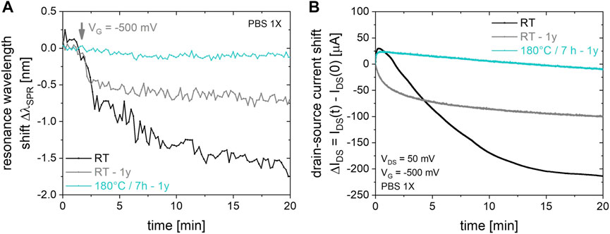
FIGURE 4. Evaluation of long-term stability on the real-time measurement of the resonance wavelength shift (A) and the drain-source current shift (B) after 1 year of storage for untreated FO-SPR gates after sputtering (RT) and after thermal exposure to 180°C for 7 h respectively.
4 Conclusion
In summary, we have shown that thermal treatment of FO tips offers a superior stabilization of the simultaneous optical and electronic readout when such tips are used as gate electrode in a FO-SPR/FET platform. The morphological changes induced by such thermal annealing prevent undergoing of further changes in the thin gold film when a gate voltage is applied upon the FET readout. Hence this approach provides a reliable and stable dual SPR/FET response which eliminates the need for long preconditioning periods commonly used for establishing a stable baseline prior to the experiment. Furthermore, the improved stability is preserved even after 1 year storage of the FO tips in argon atmosphere. Such minimizing of spontaneous “self-annealing” during the storage ensures a comparable performance of the FO-SPR gates for carrying out measurements that span over long time periods. This provides an attractive alternative to surface passivation for studies where a pre-functionalization of the gold surface with a thiol SAM is not possible, such as in electro-polymerization studies of ultrathin and degradable polymeric films [46]. Furthermore, such FO tips are expected to exhibit improved stability when used in combination with electrochemical methods, including the combination of SPR with synchronized cyclic voltammetry [47]. We found that thermal annealing at 180°C for 2 h after deposition of the thin gold film improved signal stability yet did not significantly compromise the other key characteristics of the electronic and optical transducer readout. Additionally, Faradaic contributions could be reduced by adjustments of the gate surface morphology. We envision this FO-SPR gate optimization as an essential modification for the FO-SPR/FET platform to allow real-time dual-mode investigation of surface-bound reactions under flow conditions.
Data availability statement
The datasets presented in this study can be found in online repositories. The names of the repository/repositories and accession number(s) can be found below: DOI: 10.5281/zenodo.7716920.
Author contributions
All authors listed have made a substantial, direct, and intellectual contribution to the work and approved it for publication.
Funding
This project has received funding from the European Union’s Horizon 2020 Research and Innovation Programme under the Marie Skłodowska-Curie grant agreement No. 813863–BORGES. We further thank the office of the Federal Government of Lower Austria, K3-Group–Culture, Science and Education, for their financial support as part of the project “Responsive Wound Dressing”. We gratefully acknowledge the financial support from the Austrian Research Promotion Agency (FFG; 888067).
Acknowledgments
We thank the Electron Microscopy Facility at IST Austria for their support with sputter coating the FO tips and Bernhard Pichler from AIT for software development to facilitate data evaluation.
Conflict of interest
The authors declare that the research was conducted in the absence of any commercial or financial relationships that could be construed as a potential conflict of interest.
Publisher’s note
All claims expressed in this article are solely those of the authors and do not necessarily represent those of their affiliated organizations, or those of the publisher, the editors and the reviewers. Any product that may be evaluated in this article, or claim that may be made by its manufacturer, is not guaranteed or endorsed by the publisher.
Supplementary material
The Supplementary Material for this article can be found online at: https://www.frontiersin.org/articles/10.3389/fphy.2023.1202132/full#supplementary-material
References
1. Homola J. Surface plasmon resonance sensors for detection of chemical and biological species. Chem Rev (2008) 108(2):462–93. doi:10.1021/cr068107d
2. Torricelli F, Adrahtas DZ, Bao Z, Berggren M, Biscarini F, Bonfiglio A, et al. Electrolyte-gated transistors for enhanced performance bioelectronics. Nat Rev Methods Primers (2021) 1(1):66. doi:10.1038/s43586-021-00065-8
3. Saftics A, Kurunczi S, Peter B, Szekacs I, Ramsden JJ, Horvath R. Data evaluation for surface-sensitive label-free methods to obtain real-time kinetic and structural information of thin films: A practical review with related software packages. Adv Colloid Interf Sci (2021) 294:102431. doi:10.1016/j.cis.2021.102431
4. Soltermann F, Struwe WB, Kukura P. Label-free methods for optical in vitro characterization of protein–protein interactions. Phys Chem Chem Phys (2021) 23(31):16488–500. doi:10.1039/d1cp01072g
5. Xu S, Zhan J, Man B, Jiang S, Yue W, Gao S, et al. Real-time reliable determination of binding kinetics of DNA hybridization using a multi-channel graphene biosensor. Nat Commun (2017) 8(1):14902. doi:10.1038/ncomms14902
6. Bonazza C, Zhu J, Hasler R, Mastrogiacomo R, Pelosi P, Knoll W. Responses of the pheromone-binding protein of the silk moth Bombyx mori on a graphene biosensor match binding constants in solution. Sensors (2021) 21(2):499. doi:10.3390/s21020499
7. Hall WP, Modica J, Anker J, Lin Y, Mrksich M, Van Duyne RP. A conformation- and ion-sensitive plasmonic biosensor. Nano Lett (2011) 11(3):1098–105. doi:10.1021/nl103994w
8. Kim Y, Inoue Y, Hasegawa H, Yoshida Y, Sakata T. In situ electrical monitoring of methylated DNA based on its conformational change to G-quadruplex using a solution-gated field-effect transistor. Anal Chem (2021) 93(49):16709–17. doi:10.1021/acs.analchem.1c04466
9. Scotto J, Cantillo AL, Piccinini E, Fenoy GE, Allegretto JA, Piccinini JM, et al. Using graphene field-effect transistors for real-time monitoring of dynamic processes at sensing interfaces. Benchmarking performance against surface plasmon resonance. ACS Appl Electron Mater (2022) 4(8):3988–96. doi:10.1021/acsaelm.2c00624
10. Aspermair P, Ramach U, Reiner-Rozman C, Fossati S, Lechner B, Moya SE, et al. Dual monitoring of surface reactions in real time by combined surface-plasmon resonance and field-effect transistor interrogation. J Am Chem Soc (2020) 142(27):11709–16. doi:10.1021/jacs.9b11835
11. Hasler R, Reiner-Rozman C, Fossati S, Aspermair P, Dostalek J, Lee S, et al. Field-effect transistor with a plasmonic fiber optic gate electrode as a multivariable biosensor device. ACS Sens (2022) 7(2):504–12. doi:10.1021/acssensors.1c02313
12. Verma R, Gupta BD. Detection of heavy metal ions in contaminated water by surface plasmon resonance based optical fibre sensor using conducting polymer and chitosan. Food Chem (2015) 166:568–75. doi:10.1016/j.foodchem.2014.06.045
13. Dahlin AB, Sannomiya T, Zahn R, Sotiriou GA, Vörös J. Electrochemical crystallization of plasmonic nanostructures. Nano Lett (2011) 11(3):1337–43. doi:10.1021/nl104424q
14. Dahlin AB, Zahn R, Vörös J. Nanoplasmonic sensing of metal–halide complex formation and the electric double layer capacitor. Nanoscale (2012) 4(7):2339. doi:10.1039/c2nr11950a
15. Porath D, Bar-Sadeh E, Wolovelsky M, Grayevsky A, Goldstein Y, Millo O. Annealing study of gold films using scanning tunneling microscopy. J Vacuum Sci Tech A: Vacuum, Surf Films (1995) 13(3):1165–70. doi:10.1116/1.579855
16. Karakouz T, Holder D, Goomanovsky M, Vaskevich A, Rubinstein I. Morphology and refractive index sensitivity of gold island films. Chem Mater (2009) 21(24):5875–85. doi:10.1021/cm902676d
17. Pavaskar P, Hsu IK, Theiss J, Hsuan Hung W, Cronin SB. A microscopic study of strongly plasmonic Au and Ag island thin films. J Appl Phys (2013) 113(3):034302. doi:10.1063/1.4775784
18. Antohe (Arghir) I, Schouteden K, Goos P, Delport F, Spasic D, Lammertyn J. Thermal annealing of gold coated fiber optic surfaces for improved plasmonic biosensing. Sensors Actuators B: Chem (2016) 229:678–85. doi:10.1016/j.snb.2016.02.034
19. Arghir I, Spasic D, Verlinden BE, Delport F, Lammertyn J. Improved surface plasmon resonance biosensing using silanized optical fibers. Sensors Actuators B: Chem (2015) 216:518–26. doi:10.1016/j.snb.2015.04.069
20. Torabi S, Cherry M, Duijnstee EA, Le Corre VM, Qiu L, Hummelen JC, et al. Rough electrode creates excess capacitance in thin-film capacitors. ACS Appl Mater Inter (2017) 9(32):27290–7. doi:10.1021/acsami.7b06451
21. Reiner-Rozman C, Hasler R, Andersson J, Rodrigues T, Bozdogan A, Bintinger J, et al. The top performer: Towards optimized parameters for reduced graphene oxide uniformity by spin coating. Micro Nano Lett (2021) 16(8):436–42. doi:10.1049/mna2.12070
22. Gao X, Edens G J, Hamelin A, Weaver MJ. Charge-dependent atomic-scale structures of high-index and (110) gold electrode surfaces as revealed by scanning tunneling microscopy. Surf Sci (1994) 318(1–2):1–20. doi:10.1016/0039-6028(94)90336-0
23. Chan HSO, Ho PKH, Zhou L, Luo N, Ng SC, Li SFY. In situ atomic force microscopy of the electrochemical dissolution of a copper grain. Langmuir (1996) 12(10):2580–6. doi:10.1021/la950918h
24. Hoogvliet JC, Dijksma M, Kamp B, van Bennekom WP. Electrochemical pretreatment of polycrystalline gold electrodes to produce a reproducible surface roughness for self-assembly: A study in phosphate buffer pH 7.4. Anal Chem (2000) 72(9):2016–21. doi:10.1021/ac991215y
25. Nan L, Allan D, Gang-yu L. In situ STM study of thermal annealing of Au thin films: An investigation on decay of nanometer Au clusters and 2D islands. Acta Phys Sin (Overseas Edn) (1997) 6(7):531–49. doi:10.1088/1004-423x/6/7/009
26. Gimpl ML, McMaster AD, Fuschillo N. Amorphous oxide layers on gold and nickel films observed by electron microscopy. J Appl Phys (1964) 35(12):3572–5. doi:10.1063/1.1713272
27. Beszeda I, Szabó IA, Gontier-Moya EG. Morphological evolution of thin gold films studied by Auger electron spectroscopy in beading conditions. Appl Phys A (2004) 78(7):1079–84. doi:10.1007/s00339-003-2170-0
28. Lin TS, Chung YW. Measurement of the activation energy for surface diffusion in gold by scanning tunneling microscopy. Surf Sci (1989) 207(2–3):539–46. doi:10.1016/0039-6028(89)90140-4
29. Kolomenski A, Kolomenskii A, Noel J, Peng S, Schuessler H. Propagation length of surface plasmons in a metal film with roughness. Appl Opt (2009) 48(30):5683. doi:10.1364/ao.48.005683
30. Kanso M, Cuenot S, Louarn G. Roughness effect on the SPR measurements for an optical fibre configuration: Experimental and numerical approaches. J Opt A: Pure Appl Opt (2007) 9(7):586–92. doi:10.1088/1464-4258/9/7/008
31. Heinz R. Surface plasmons on smooth and rough surfaces and on gratings, X. Heidelberg: Springer Berlin (1988). p. 136.
32. Lee K, Lue JT. Annealing effect on the optical properties of gold films deposited on silicon substrates. Appl Opt (1988) 27(6):1210. doi:10.1364/ao.27.001210
33. Douglass EF, Driscoll PF, Liu D, Burnham NA, Lambert CR, McGimpsey WG. Effect of electrode roughness on the capacitive behavior of self-assembled monolayers. Anal Chem (2008) 80(20):7670–7. doi:10.1021/ac800521z
34. Zhao YP, Wang GC, Lu TM, Palasantzas G, De Hosson J. Surface-roughness effect on capacitance and leakage current of an insulating film. Phys Rev B (1999) 60(12):9157–64. doi:10.1103/physrevb.60.9157
35. Giovannitti A, Rashid RB, Thiburce Q, Paulsen BD, Cendra C, Thorley K, et al. Energetic control of redox-active polymers toward safe organic bioelectronic materials. Adv Mater (2020) 32(16):1908047. doi:10.1002/adma.201908047
36. Leonardi F, Tamayo A, Casalini S, Mas-Torrent M. Modification of the gate electrode by self-assembled monolayers in flexible electrolyte-gated organic field effect transistors: Work function vs. capacitance effects. RSC Adv (2018) 8(48):27509–15. doi:10.1039/c8ra05300f
37. Gao P, Weaver MJ. Metal-adsorbate vibrational frequencies as a probe of surface bonding: Halides and pseudohalides at gold electrodes. J Phys Chem (1986) 90(17):4057–63. doi:10.1021/j100408a045
38. Kolb DM. Electrochemical surface science. Angew Chem Int Ed (2001) 40(7):1162–81. doi:10.1002/1521-3773(20010401)40:7<1162::aid-anie1162>3.0.co;2-f
39. Abelès F, Lopez-Rios T, Tadjeddine A. Investigation of the metal-electrolyte interface using surface plasma waves with ellipsometric detection. Solid State Commun (1975) 16(7):843–7. doi:10.1016/0038-1098(75)90876-5
40. Novo C, Mulvaney P. Charge-induced Rayleigh instabilities in small gold rods. Nano Lett (2007) 7(2):520–4. doi:10.1021/nl062649t
41. Hasler R, Vísová I, Vrabcová M, Houska M, Spasovová M, Lísalová H, et al. Fiber optic probe with antifouling polymer brush biointerface for bi-modal biosensing in complex liquid samples. In: Biophotonics in point-of-care II. Strasbourg, France: Proc. SPIE 12145 (2022). p. 1214505.
42. Stangl M, Militzer M. Modeling self-annealing kinetics in electroplated Cu thin films. J Appl Phys (2008) 103(11):113521. doi:10.1063/1.2937249
43. Lee H, Nix WD, Wong SS. Studies of the driving force for room-temperature microstructure evolution in electroplated copper films. J Vac Sci Technol B (2004) 22(5):2369. doi:10.1116/1.1788680
44. Ying A, Witt C, Jordan-Sweet J, Rosenberg R, Noyan IC. A quantitative analysis of room temperature recrystallization kinetics in electroplated copper films using high resolution x-ray diffraction. J Appl Phys (2011) 109(1):014907. doi:10.1063/1.3514096
45. Willey TM, Vance AL, van Buuren T, Bostedt C, Terminello LJ, Fadley CS. Rapid degradation of alkanethiol-based self-assembled monolayers on gold in ambient laboratory conditions. Surf Sci (2005) 576(1–3):188–96. doi:10.1016/j.susc.2004.12.022
46. Marchesi D’Alvise T, Sunder S, Hasler R, Moser J, Knoll W, Synatschke CV, et al. Preparation of ultrathin and degradable polymeric films by electropolymerization of 3-amino- l -tyrosine. Macromol Rapid Commun (2022) 2200332. doi:10.1002/marc.202200332
Keywords: fiber optic, surface plasmon resonance, field-effect transistor, annealing, signal stabilization, real-time sensing
Citation: Hasler R, Steger-Polt M-H, Reiner-Rozman C, Fossati S, Lee S, Aspermair P, Kleber C, Ibáñez M, Dostalek J and Knoll W (2023) Optical and electronic signal stabilization of plasmonic fiber optic gate electrodes: towards improved real-time dual-mode biosensing. Front. Phys. 11:1202132. doi: 10.3389/fphy.2023.1202132
Received: 07 April 2023; Accepted: 04 July 2023;
Published: 14 July 2023.
Edited by:
Chao Liu, Northeast Petroleum University, ChinaReviewed by:
Satyendra Kumar Mishra, Technical University of Denmark, DenmarkRoli Verma, Tel Aviv University, Israel
Mubarak A. Mujawar, Florida International University, United States
Copyright © 2023 Hasler, Steger-Polt, Reiner-Rozman, Fossati, Lee, Aspermair, Kleber, Ibáñez, Dostalek and Knoll. This is an open-access article distributed under the terms of the Creative Commons Attribution License (CC BY). The use, distribution or reproduction in other forums is permitted, provided the original author(s) and the copyright owner(s) are credited and that the original publication in this journal is cited, in accordance with accepted academic practice. No use, distribution or reproduction is permitted which does not comply with these terms.
*Correspondence: Roger Hasler, Roger.Hasler@dp-uni.ac.at; Wolfgang Knoll, wolfgang.knoll@ait.ac.at