Effects of thermal treatment on the complex structure of luminescence emission of Li-doped ZnO screen-printed films
 O. Chukova1,2*
  L. Borkovska3
  L. Khomenkova3,4
  N. Korsunska3
  S. Ponomaryov3
  M. Androulidaki5
  E. Stratakis5
- 1Deutsches Elektronen-Synchrotron (DESY), Hamburg, Germany
- 2Faculty of Physics, Taras Shevchenko National University of Kyiv, Kyiv, Ukraine
- 3V. Lashkaryov Institute of Semiconductor Physics, National Academy of Sciences of Ukraine, Kyiv, Ukraine
- 4National University “Kyiv Mohyla Academy”, Kyiv, Ukraine
- 5Institute of Electronic Structure and Laser, Foundation for Research and Technology Hellas (IESL-FORTH), Heraklion, Greece
The ZnO–Li films were synthesized and investigated in an attempt to explore and develop RE-free phosphor materials capable of emitting intense visible light in a wide spectral range. The effects of both heterovalent doping with lithium and high-temperature annealing on the optical properties of ZnO films were studied. The films were deposited on the Al2O3 substrate using the screen-printing method and annealed at 800–1,000°C in air for 0.5–3 h. Both doping and annealing result in the transformation of the shape of reflectance spectra in the range of 300–400 nm and the shift of absorption edge to the long-wavelength region. At the same time, the bandgap value estimated taking into account the exciton peak position and its binding energy is independent of Li-doping. The feature at 300–400 nm and the shift of absorption edge are ascribed to the appearance of the absorption band that excited the yellow photoluminescence band. The photoluminescence spectra of undoped and Li-doped films show the emission bands in the ultraviolet and visible spectral ranges. The ultraviolet emission is due to ZnO exciton recombination. The visible emission band comprises several components peaked at 430, 482, 540, 575, and 640 nm. Their relative intensities depend on Li-doping, annealing temperature, and annealing duration. The 430- and 482-nm luminescence bands were observed in Li-doped films only. Their excitation spectra show the peak located at 330–340 nm, indicating that the energy significantly exceeds the ZnO bandgap energy. Consequently, the 430- and 482-nm luminescence bands are attributed to an additional crystal phase formed under annealing. Other components of visible emission bands are ascribed to the defect-related emission of ZnO. The possible nature of these bands is further discussed. Li-doping and annealing at intermediate temperatures result in blue emission and an enhancement of other visible bands, which makes ZnO–Li films a perspective material in photonic applications.
1 Introduction
Earth-abundant materials suitable for several modern applications have attracted great interest due to the development of eco-friendly and low-cost basic compounds for electronic devices. The most promising earth-abundant materials currently considered for solar energy production and optoelectronic applications include (but will not be limited to) sulfides/selenides, nitrides, phosphides, and oxides [1–5]. Optoelectronics needs the development of earth-abundant luminescent materials instead of rare-earth-activated luminophores that are currently used in many devices because the high-technology and environmental applications of the RE elements have grown dramatically in diversity and importance over the last 4 decades [6–8]. However, there are some applications for which the usage of RE ions is critical and cannot be substituted with alternative elements. As such substitution is possible for luminescent applications, the search for RE-free luminescent materials becomes a significant task. For a long time, ZnO-based materials have attracted considerable attention for possible applications in optoelectronic devices, particularly in the ultraviolet (UV) light emitters [9–12]. Visible-light-emitting materials with various spectral properties could also be obtained on the basis of ZnO because both blue luminescence and green luminescence have already been reported in the modified ZnO structures [13–17]. The presence of several visible emission bands can be useful for the development of white-light-emitting device. Additionally, the ZnO matrix seems promising due to its cheap and non-toxic constituting compounds. For this purpose, the enhancement of visible emission bands is considered more appropriate. To achieve this, two approaches can be considered: i) increasing the intensity of self-activated photoluminescence (PL) via different treatments and ii) doping ZnO with different impurities. In addition, the investigation of the effect of various treatments on PL spectra of these materials can help identify the nature of different emission centers.
Meanwhile, the origin of different visible emission bands in ZnO compounds is investigated occasionally, and they are not fully assumed. Such a situation leads to different controversial hypotheses in the literature [17]. It was clearly shown that the bands of visible luminescence of ZnO are connected with the structural defects of their crystal lattice [17–21]. It was established that the short-wavelength visible emission of ZnO is correlated with the density of interstitial zinc (Zni) defects [19–21]. Transitions from Zni shallow defect levels to the top of the valence band are usually ascribed to the violet emission band at approximately 400–415 nm [17, 21–23]. However, some authors ascribed the noted transition to the blue emission band at 430–440 nm [19, 20]. Another possible explanation of the blue band is the transition from the conduction band to the deep defect levels related to Zn vacancies (VZn) [15, 21–23]. Green luminescence bands centered near 480–490 nm and 530–540 nm were ascribed to the defect centers induced by oxygen vacancies (VO) [15, 17, 22], zinc interstitials [24], and zinc vacancies [25, 26]. In addition, some authors have found other emission bands connected with interstitial oxygen (Oi) atoms [21–23].
To separate the contribution of different bands, a selective excitation can be applied. This approach was used in [19, 20], where several sub-bands in the blue emission of the ZnO nanoparticles peaked near 415, 440, 455, and 488 nm were observed and assigned to different sub-states of the Zni and ex-Zni defect centers. However, the determination of the contribution of different emission bands to the complex PL spectrum and the effect of various factors on PL spectrum shape along with the elucidation of the emission origin still remains a challenge.
It is known that the structural, optical, and electrical properties of ZnO materials can be modified by doping them with the heterovalent impurities. For instance, the implantation of single-valence ions (H+, Li+, and Cu+) induces blue and green emission bands in the ZnO-based materials [27–29]. It is interesting that doping with Li+ can also affect the ZnO sample structure. Particularly, it can suppress or promote the growth of ZnO particles during their synthesis as well as control the grain sizes in the polycrystalline ZnO films and ceramics upon annealing [30].
Among different approaches used for the fabrication of ZnO materials, the screen-printing technique was considered appropriate in this work due to its simplicity and low cost [31–33]. In the present work, the optical and light-emitting properties of Li-doped ZnO films fabricated using the screen-printing approach were investigated versus annealing treatment using different excitation light wavelengths and the temperature of measurements.
2 Synthesis of the films and experiment
2.1 Samples
The studied ZnO films were fabricated using the screen-printing technique [31–33] on Al2O3 (R-plane) substrates with the dimension of 1 × 1 cm2 and thickness of 1 mm. The substrates were consecutively cleaned in acetone, alcohol, and water. Cleaning in water was carried out in an ultrasound bath at 60°C for 30 min. The corresponding pastes for printing were prepared using ZnO powder (99.99%) from Sigma-Aldrich. The powder was mixed with distilled H2O or LiNO3:H2O solutions and milled with agate balls. The printing process was performed under ambient conditions with a 45° deflection angle and less than 1 mm distance between the applying wing and the substrate. After drying under normal conditions for 24 h, the samples were annealed at TA = 800°C, 900°C, and 1,000°C for tA = 0.5, 1, 2, and 3 h in air. The thickness of sintered films was approximately 40 μm. The Li content in the films was [Li] = 0.3 wt%.
2.2 Experimental methods
The morphology and chemical composition of the samples were investigated using a JAMP-9500F (JEOL) tool equipped with EDX and an Auger microprobe. The spatial resolution in the secondary electron image mode was 3 nm. The microprobe was equipped with a sensitive hemispheric Auger spectrometer with energy resolution ΔE/E ranging from 0.05% to 0.6% and an ion-etching gun for layer-by-layer analysis with the Ar+ ion beam diameter of 120 μm, capable of moving by raster of dimension 1 × 1 mm. The variation range of the Ar+ ion beam energy is from 0.01 to 4 keV, while minimal beam current is 2 μA with 3 keV. To obtain chemical maps using the EDX method, preliminary etching with Ar ions was used to remove the surface layer of approximately 100 nm and to clean the samples from contamination. The UV-vis reflectance spectra of the samples were measured using the PerkinElmer LAMBDA 950 spectrometer. In the used mode, the monochromator was placed before the samples, and all light reflected from the sample surface was collected using the photometric sphere. The photoluminescence (PL) spectra were investigated using an ACTONi (500) monochromator with grating 150 grooves/mm (blaze @ 300 nm), slit on 50 micron, and liquid N2-cooled CCD registration. The PL excitation (PLE) spectra were investigated using an SDL-2 monochromator with grating 600 grooves/mm, slit on 200 micron, and PMT registration. The PL spectra were excited with a 325-nm diode laser or powerful xenon lamp (325 and 375 nm). The spectra were corrected on the spectral response of the setups. The temperature of measurements was 4.2 K, 15–80 K, and 300 K. All samples were placed simultaneously in the cryostat system given the opportunity for correct comparison of their PL properties.
3 Results
3.1 SEM and EDX study of the films
The SEM and EDX data for ZnO and annealed ZnO–Li films are shown in Figure 1. All the films consist of the sintered grains with the sizes varying in the range of 0.5–1.5 microns (Figure 1, insets). In addition, no additional binder was used in ZnO-based pastes, which led to the formation of pores. However, the ZnO–Li films are of lower porosity than their ZnO counterparts. Thus, one can suppose that Li-doping favors better sintering of the films. The EDX study of ZnO films revealed the presence of Zn and O elements (Figure 1, curve 1). The presence of Al was also detected in ZnO–Li films (Figure 1, curve 2). One can assume that Li favors the penetration of Al from underlying sapphire substrates into the films’ volume. At the same time, the Li signal in EDX spectra is absent due to the Be window using in the SEM/EDX setup. It is worth noting that in our previous study, the presence of Li ions in the films prepared using the approach described above was revealed using the SIMS method (not shown here), and it was found that Li content changed insignificantly with annealing treatment.
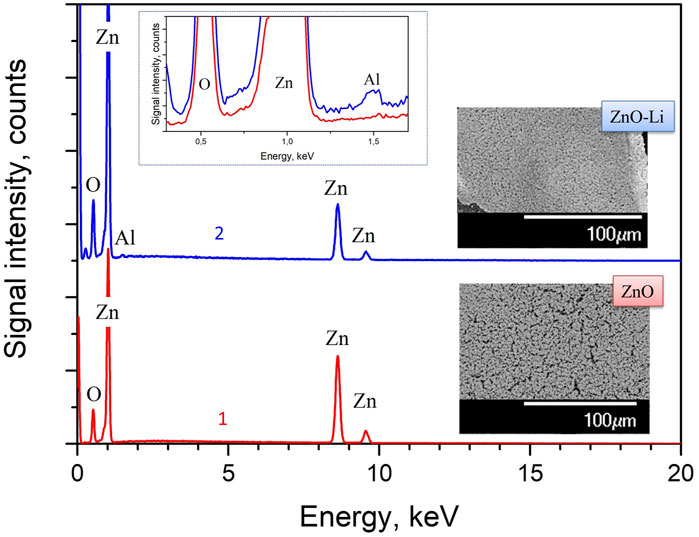
FIGURE 1. EDX data for ZnO (1) and ZnO–Li (2) films annealed at 1,000°C for 1 h in air. The insets show the SEM COMPO images of the surface of these films and enlarged EDX spectra for 0.3–1.7 keV range.
3.2 Reflectance spectra
Room-temperature UV-vis reflectance spectra of the undoped ZnO films annealed at TA = 800°C demonstrate high reflectivity in the visible spectral range with sharp absorption edge near 380 nm. The spectra also show some peculiarities in the 300–375 nm spectral range (Figure 2A). In the samples annealed at higher temperatures (1,000°C), only the sharp edge is detected (Figure 2,a, curve 1). Thermal treatment also results in the transformation of the reflectance spectra of ZnO–Li films. The films annealed at 900 and 1,000°C for 30 min have shown the shift of the long-wavelength absorption edge toward ∼405 nm (Figure 2A). The reflectance spectra of all annealed ZnO–Li films show the peculiarities in the 300–400 nm spectral range (Figure 2) whose contribution changes non-monotonically with annealing time (Figure 2B). The comparison of undoped and Li-doped ZnO films shows that doping with Li results in the appearance of additional reflectance minimum near 390–400 nm, whose contribution increases with the increase in annealing temperature and time. In addition, the additional features at lower wavelength were observed.
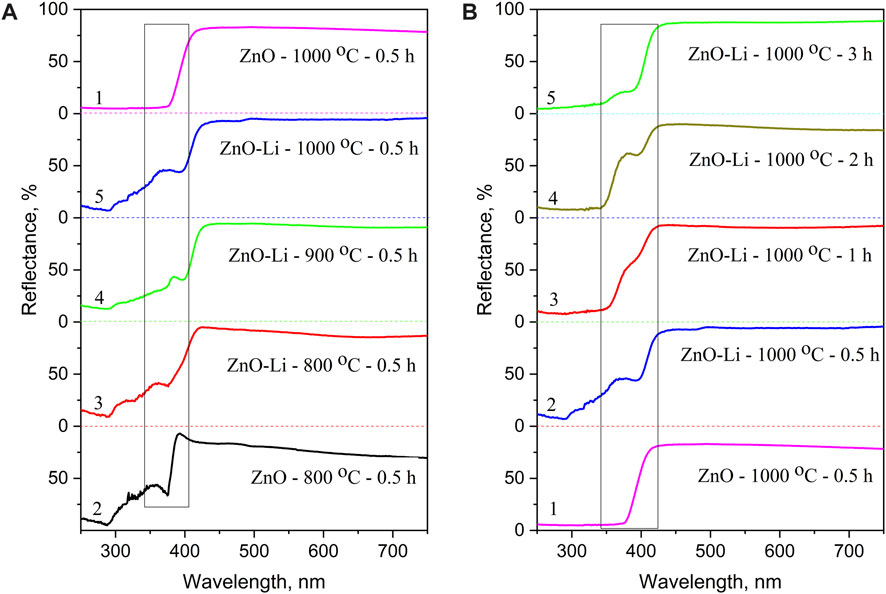
FIGURE 2. UV-vis reflectance spectra: (A) undoped (1,2) and Li-doped ZnO films (3–5) annealed for 30 min at 800 (2, 3), 900 (4), and 1,000°C (1,5); (B) undoped (1) and Li-doped ZnO (2–5) films annealed at 1,000°C for 0.5 (2), 1 (3), 2 (4), and 3 h (5).
3.3 Luminescence
The room-temperature photoluminescence spectra of undoped ZnO films are complex and consist of the narrow UV band (in the 350–420 nm range) and wide visible band (in the 430–800 nm range). The former is ascribed to exciton emission, and the latter is ascribed to the defect-related band. The intensities of these PL bands depend on annealing treatment, excitation wavelength, and temperature of measurements. The typical spectrum of the films annealed at TA = 800°C for tA = 0.5 h is shown in Figure 3. It demonstrates an intense UV band and visible band of low intensity. An annealing at TA = 900 and 1,000°C results in the UV band quenching and the enhancement of the visible band with a peak position at 530–560 nm (Figure 3), which is similar to situations observed in [30] for the screen-printed ZnO film. In Li-doped ZnO films, UV emission is significantly lower than the visible emission, and for the most of the samples, it is hardly registered (Figure 3).
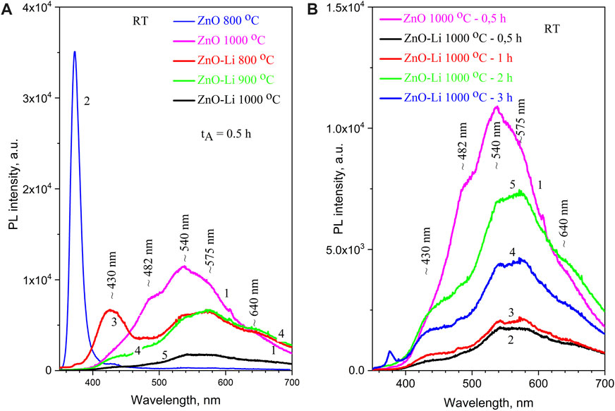
FIGURE 3. Room-temperature PL spectra: (A) ZnO (1,2) and ZnO–Li (3–5) films annealed at 800 (2,3), 900 (4), and 1,000°C (1,5) for 0.5 h; (B) ZnO (1) and ZnO–Li (2-5) films annealed at 1,000°C for 0.5 (2), 1 (3), 3 (4), and 2 h (5). The excitation wavelength is 325 nm.
The analysis of PL spectra reveals their multicomponent nature. Several PL bands with the peaks near ∼430, ∼482, ∼540 (intensive), ∼575 (the most intensive), and ∼640 nm (weak) can be distinguished. Most of them show similar variations with annealing temperature and duration. However, the intensity of the 430 nm band strongly decreases with TA increase (Figure 3).
The low-temperature PL spectra of undoped and Li-doped samples are shown in Figure 4 and Figure 5. In the UV spectral range (350–420 nm), the peaks that are usually ascribed to zero-phonon lines and phonon replica of free- and donor-bound excitons in ZnO at ∼368.5, ∼374.5, ∼383, and ∼391 nm are observed [30]. These peaks are characterized by different rates of temperature quenching. Figure 3,a shows that in ZnO–Li samples annealed at 800°C, the intensity of the 368.5-nm peak decreases with temperature more significantly (decreases six times with a temperature increase from 16 to 80 K) than the intensity of other three peaks (the 374.5-nm and 383-nm peaks decreased by 2 and 1.2 times, respectively). It should also be emphasized that the relative contribution of UV emission to the total PL spectra of Li-doped films increases with the decrease in measurement temperature (Figure 4; Figure 5). At room temperature, this band is observed as a weak component only in the spectra of ZnO–Li films annealed at 800°C (Figure 4B).
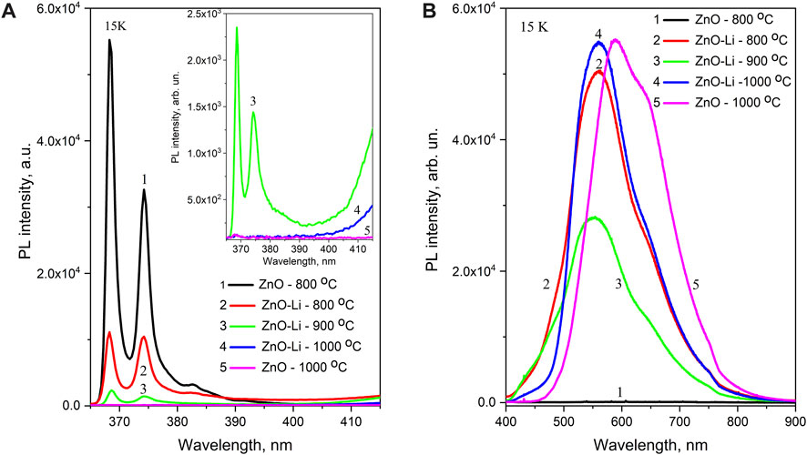
FIGURE 4. PL spectra recorded at 15 K for ZnO and ZnO–Li films annealed at 800 (1,2), 900 (3), and 1,000°C (4,5) for 0.5 h and presented for 365–415 nm (A) and 400–900 nm (B) spectral ranges. The excitation wavelength is 325 nm. The inset in (A) shows the UV exciton emission for ZnO (5) and ZnO–Li (3,4) films annealed at 900°C (3) and 1,000°C (4,5).
At low temperatures, the intensity of the 350–420 nm emission band in the spectra of ZnO–Li films annealed at 800°C is 3–4 times higher than the intensity of the 430–800 nm band (Figure 5A). The comparably weak 350–420 nm band is also observed in the low-temperature spectra of ZnO–Li films annealed at 900°C (Figure 5B). For ZnO–Li films annealed at 1,000°C, the 350–420 nm band is not observed even at low temperatures (Figure 5C). Thus, we can assume that the increase in annealing temperature of the ZnO–Li films leads to the decrease in contribution of 350–420 nm emission bands to their total emission spectra.
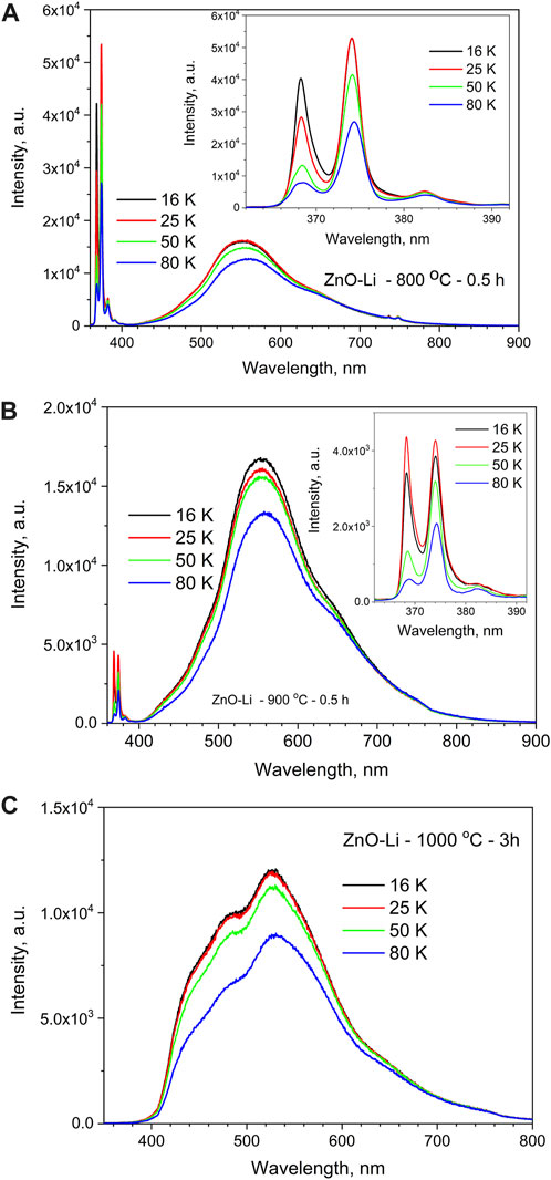
FIGURE 5. PL emission spectra of the ZnO–Li films annealed at 800°C for 0.5 h (A), 900°C for 0.5 h (B), and 1,000°C for 3 h (C) and recorded under 325 nm laser excitation at different temperatures. Insets in (A) and (B) show the exciton-related PL bands in the UV spectral range.
The low-temperature spectra of the visible emission band comprise of five components mentioned above, but, unfortunately, these components remain wide and strongly overlapped even at 16 K (Figure 5, a–4, c). The relative contributions of all the five components of the films annealed at 800°C and 900°C do not depend on temperature in the 16–50 K range. Their intensity slightly decreases with the increase in temperature from 50 K. However, the low-temperature spectra of ZnO–Li films annealed at 1,000°C differ from their spectra measured at room temperature. The main difference lies in the considerable decrease in contribution of the 575-nm component to the total spectra. The contribution of the 540-nm component also decreases, but it is difficult to estimate its rate due to a strong mutual overlapping of all the components even at low temperatures (Figure 2, c; 4, c).
The excitation spectra of the wide visible PL band recorded at different wavelengths near the peak positions of its components (Figure 6) comprised several strongly overlapped bands with maxima at approximately 330–335 nm, 345–350 nm, and 380 nm. The first excitation band is found only for 430 and 485 nm PL bands, and the remaining two are observed only at the 540- and 575-nm PL bands. In fact, the low-temperature emission spectrum of Li-doped films recorded under 375 nm excitation shows a maximum near 580 nm and shoulders at 510 and 640 nm, while under 325 nm excitation, emissions in the blue–green spectral range increases strongly, shifting the PL peak to 500 nm (Figure 7). The excitation maximum at 345–350 nm corresponds to energies close to the bandgap energy of ZnO and can be explained by band-to-band transitions in ZnO. This means that at least the green and yellow–red PL bands originated from ZnO. It should also be noted that these PL bands are different from blue and cyan PL bands due to their dependence of the PL intensity on excitation power. In particular, the comparison of the PL spectra of the same Li-doped film recorded under excitation using laser (Figure 5C) and xenon lamp (Figure 6) light shows that the PL intensity of the 540 nm emission band increases more with excitation power than that of 430 and 482 nm bands.
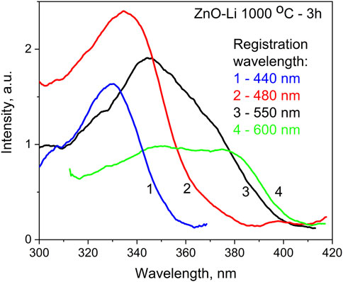
FIGURE 6. Excitation spectra for the ZnO–Li films annealed at 1,000°C for 3 h. Spectra recorded at 4.2 K for 440, 480, 550, and 600 nm.
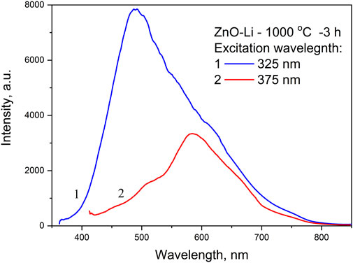
FIGURE 7. Emission spectra of the same films recorded at 4.2 K under the excitation using a xenon lamp at 325 and 375 nm wavelengths.
4 Discussion
4.1 Effects of Li-doping on the optical properties of the films
UV-vis diffuse reflectance spectra of the investigated Li-doped films have revealed two main phenomena: an appearance of spectral features in the 300–400 nm spectral range and a shift of absorption edge toward longer wavelengths. The first phenomenon is a result of an optical scheme used for experiments. In this scheme, the monochromator is placed before the sample. The light of a certain wavelength selected by a monochromator reaches the sample, then reflects, and is collected by the diffuse sphere. If the sample luminesces, then emission is also collected together with the reflected light. Therefore, in case of intense luminescence, the detected spectra will be a sum of reflectance and PL excitation spectra. In particular, the feature at approximately 320–330 nm in the reflectance spectra of the ZnO–Li film (Figure 2) is a result of luminescence contribution, which is in agreement with PLE spectra detected at 600 nm (Figure 6). The comparison of the reflectance spectra in the UV spectral range (300–400 nm) with PL excitation spectra recorded at specific registration wavelengths (Figure 8) confirms the proposed explanation. Indeed, for both undoped and Li-doped films, various bands found in the UV range in the reflectance spectra are in good agreement with those observed in PL excitation spectra.
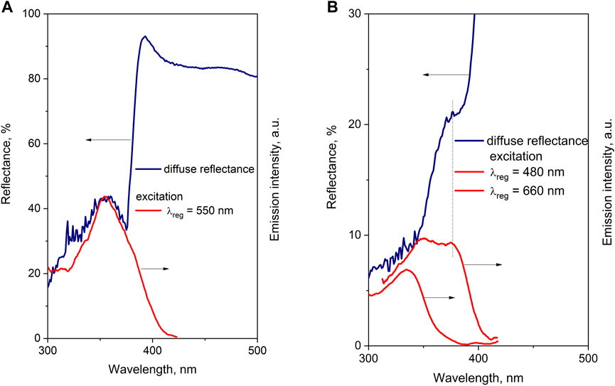
FIGURE 8. Comparison of reflectance spectra of the ZnO film annealed at 800 C (A) and reflectance spectra of the ZnO–Li film annealed at 1000 C for 3 h (B) and excitation spectra of the ZnO–Li film annealed at 1000 C for 3 h.
The presence of the 390 nm feature in the reflectance spectra (Figure 8) significantly changes the absorption edge for the Li-doped films. Apart from this, no exciton feature was found in the reflectance spectra of both the undoped and doped samples annealed at 1,000°C (Figure 2). This can be caused by the significant contribution of band tail absorption that shows an Urbach behavior. Two main remarks follow from the discussed feature of the measured reflectance spectra: i) the reflectance peaks observed in the setup described in this study correspond to the light absorption participated in the luminescence excitation; ii) particularly, for ZnO materials, the contribution of exciton absorption along with significant “impurity” absorption should be taken into account if it is required to estimate the bandgap energy. It is worth noting that the absorption at 390 nm observed in Li-doped films is apparently caused by an oxygen vacancy defect, as demonstrated for ZnO ceramic samples doped with group I elements [34].
In spite of different attempts made to estimate the ZnO bandgap value using well-known relationships of absorption coefficient versus energy [34, 35], it can be accurately estimated only from the exciton peak position by taking into account its binding energy (60 meV). In this study, the ZnO bandgap value of films annealed at 800oC can only be obtained from the reflectance spectra (Figure 2). However, the exciton peak position can also be extracted from PL spectra. This allows for the estimation of the bandgap value of the films annealed at both 800 and 900°C, as well as at 1,000°C, for 3 h (Figure 4). The exciton peak position was found to be similar for all these samples, which indicates that all of them have similar bandgap values despite of the effect of Li-doping on the absorption edge. The estimated bandgap values of our samples are 3.41 eV (at 16 K) and 3.35 eV (at 300 K). The latter value is close to that reported for perfect ZnO crystals (3.3 eV [36–38]).
4.2 Transformations of luminescence spectra of the Li-doped films with temperature
The emission bands in the range of 350–420 nm correspond to well-known and widely studied ZnO exciton luminescence. In the low-temperature PL spectra (Figure 4; Figure 5), the peak near 368.5 nm can be attributed to a zero-phonon line of donor-bound exciton, and the other peaks can be attributed to the phonon replica of free exciton. The increase in temperature from 16 to 80 K results in a stronger decrease in intensity of the 368.5 nm band compared to other exciton-related peaks (Figure 5) that can be explained by small binding energy of donor-bound exciton. The absence of a zero-phonon line of free exciton in the low temperature PL spectra can be explained by enhanced band tail absorption. In all Li-doped films, visible PL bands peaked at ∼430, 482, 540 (the most intensive for the annealed samples), 575 (the most intensive for the unannealed samples), and 640 nm (weak for the annealed samples) were detected (Figures 2–5). The majority of these PL bands changed in the same manner with annealing temperature and duration, except the 430-nm component whose intensity strongly decreased with the increase in annealing temperature (Figure 3B). Each PL component is discussed in the following sub-sections.
4.2.1 Blue emission
As mentioned in Introduction, there are two different opinions in the literature about the origin of the blue 430–440 nm emission band in ZnO materials. The first one considers radiative transitions from shallow Zni defect levels to the valence band [39–43]. However, the energy of the transitions from shallow Zni defect levels (located at 0.05 eV below the conduction band) cannot explain the 430-nm PL emission.
The second opinion assumes that this PL emission could originate from the carrier transition from the conduction band to VZn deep defect levels [44–46]. The level of VZn of our ZnO–Li samples estimated from the PL peak position can be approximately 0.4 eV from the top of the valence band, which is consistent with the values reported by other authors (0.3–0.5 eV) [17, 21]. Despite such an agreement, the analysis of corresponding PL excitation spectra reveals that this emission is excited by the 320–330 nm light (3.64–3.75 eV) where the energy significantly exceeds the ZnO bandgap value (3.3–3.4 eV). Thus, one can assume that 430-nm PL emission can originate from the other phase with a larger bandgap value. One of the possible reasons of the appearance of such phase can be the formation of the Li2O phase (with the bandgap of ∼7.5 eV). Another reason can be the diffusion of the substrate atoms into the film volume (for instance, Al diffusion from underlying sapphire substrate (Figure 1) and the formation of the LixAlOy phase with a bandgap of ∼4.64–4.85 eV). Similar effect was reported previously for ZnO films grown on Si substrates where the formation of Zn silicate was observed [35].
4.2.2 Cyan emission
The cyan band centered near 482 nm is observed for ZnO–Li films. The luminescence band with a close spectral position had been reported previously by several authors for ZnO [21–23, 47–50]. The reported difference in the maximum position of this band in various studies can be connected with difficulties in determining the peak position due to a considerable mutual overlapping of several visible emission bands and with some variations in the defect-level positions in different ZnO-based materials such as bulk crystals, nanocrystals, and doped films. Most of the authors attributed this cyan-green emission to oxygen vacancies (VO) in the ZnO crystal lattice and explained by the recombination of electrons at the VO level with photoexcited holes in the valence band [47–50]. At the same time, the excitation spectrum of 482-nm PL band shows the peak at approximately 335 nm which corresponds to energy larger than ZnO bandgap energy (Figure 7). In addition, it is found only in Li-doped films. Therefore, similar to the 430-nm PL band, cyan emission cannot originate from ZnO and should be ascribed to another crystal phase with larger bandgap values.
4.2.3 Green emission
The band at approximately 540 nm is the most intense band in the PL spectra of the undoped ZnO films annealed at 1,000°C (Figure 3A) and in the low-temperature PL spectra of Li-doped films (Figures 5B,C). Despite this band being observed in Li-doped films, its existence in undoped samples provides the possibility to ascribe it to native defects or uncontrolled impurities. The well-known green luminescence band in ZnO is peaked in the range of 500–530 nm and ascribed by different authors to singly ionized oxygen vacancies [15, 21–23], residual copper impurities [51], zinc vacancies [52], or complex defect including zinc interstitials [24]. It has been proposed [53] that the green PL in ZnO can be caused by transitions from two separate shallow donors to a deep acceptor. In [24], Zni shallow donors were identified as a part of complex defect responsible for a 520-nm green emission in undoped ZnO. Point Li-induced defects in the ZnO crystal lattice are interstitial Li ions (Lii) and Li cations in Zn positions (LiZn) and the former type of the defects is most probable [37]. It is likely possible that Lii defects can participate in the formation of similar defect complexes and be responsible for the 540-nm band. Two different types of Lii defects with different symmetries of their crystal (LiiO octahedral and LiiT tetrahedral) surrounding the ZnO crystal lattice were considered in [37, 38] which can explain the difference in peak positions.
Regarding our films, the residual copper impurities could be present in raw ZnO powders. Similarly, green emission was previously reported for the ZnO samples doped with Cu+, Li+, or H+ [27–29, 31, 50, 54–56]. Our experiment on ZnO ceramics doped with Cu revealed that the 540-nm PL band was enhanced with the increase in Cu content [31]. Its PL excitation spectra were similar to those recorded for Li-doped ZnO films at 540–550 nm wavelength (Figure 7). Thus, we consider that the 540-nm PL emission in our undoped and Li-doped films is rather caused by CuZn defects.
4.2.4 Yellow–red emission
Annealing at higher temperatures enhances luminescence in the yellow–red spectral region. The yellow emission band is peaked within 575–600 nm (Figures 3B,C) and clearly shows excitation via ZnO band-to-band transitions (Figure 6). In the undoped films, this emission is usually ascribed to the native defects, particularly related to interstitial oxygen (Oi) [19, 57]. This assignment was done based on the results obtained for ZnO films subjected to annealing in various atmospheres. It is considered that Oi is a deep acceptor, and its energy level is located at 0.7 or 1.5 eV above the top of the valence band [50, 58]. In our undoped films, we cannot exclude that the yellow band is related to Oi defects. At the same time, in Li-doped films, the yellow PL band is caused by the LiZn acceptor [59]. The main arguments for this assumption are as follows: i) similar PL band has been observed for ZnO–Li ceramics where it enhanced with Li content [34]; ii) in the PL excitation spectrum of the yellow band, a selective maximum at 390–400 nm is observed (Figure 6), which is similar to ZnO ceramics and layers doped with group I elements [30, 34]. It should be noted that according to our observations and results of other authors, the Li concentration in the Li-doped ZnO samples does not depend on the temperature and duration of annealing, and at least such effect was not revealed in the investigations of influence of annealing on their conductivity behavior, piezoelectric property, and ferroelectric property [60–63].
Another PL component peaked at 640 nm was observed in the undoped ZnO films annealed at 1,000°C. This band is also considered to be correlated with excess oxygen-related defects. It has been proposed that the 640-nm PL component is due to the transitions between Zni and Oi defect levels [50, 64, 65], which is doubtful taking into account the well-known energy position of the Zni defect levels (0.05 eV below the conduction band). Thus, the origin of this emission needs further investigation.
5 Conclusion
The undoped and Li-doped ZnO films were prepared using the screen-printing approach on the Al2O3 substrate and sintered at 800–1,000°C in air. It was found that the heterovalent Li-doping leads to the transformation of PL spectra, namely, the quenching of exciton UV emission (in the 350–420 nm range) and the enhancement of visible PL emission (in the 430–800 nm range). This interrelation depends on the annealing temperature and duration. Li-doping results in the transformation of the shape of reflectance spectra over the 300–400 nm range and the shift of the absorption edge toward the long-wavelength region. At the same time, the bandgap value estimated by taking into account the exciton peak position and its binding energy is found to be independent of Li-doping. The feature at 300–400 nm and the shift of absorption edge are ascribed to the appearance of the absorption band that excited the yellow PL band. For UV exciton emission, more intense quenching of the zero-phonon line of donor-bound exciton compared to the phonon replica of free exciton with temperature of measurements was observed, and the absence of a zero-phonon line of free exciton in the low temperature PL spectra was explained by enhanced band tail absorption. The visible PL band comprises several components peaked at approximately 430, 485, 540, 575, and 640 nm. Their relative intensities depend on Li-doping and regimes of thermal treatment. The yellow band at 575–600 nm is ascribed to the Oi defect centers in undoped ZnO films and LiZn defects in Li-doped films. This LiZn-related PL component is characterized by a specific PL excitation spectrum. The most intensive low-temperature PL band observed at 540 nm can be ascribed to CuZn defects present in raw materials. The 430-nm and 482-nm PL bands appearing in Li-doped films are supposed to originate from the other crystal phases of a larger bandgap value.
Data availability statement
The datasets presented in this study can be found in online repositories. The names of the repository/repositories and accession number(s) can be found at: https://bib-pubdb1.desy.de/record/597223.
Author contributions
OC: conceptualization, data curation, formal analysis, investigation, methodology, project administration, visualization, writing–original draft, validation, and writing–review and editing. LB: conceptualization, formal analysis, validation, and writing–review and editing. LK: conceptualization, data curation, investigation, validation, visualization, writing–review and editing, formal analysis, and writing–original draft. NK: formal analysis, supervision, validation, and writing–review and editing. MA: data curation, investigation, validation, and writing–review and editing. ES: funding acquisition, investigation, project administration, resources, validation, writing–review and editing, and methodology.
Funding
The author(s) declare that financial support was received for the research, authorship, and/or publication of this article. This project has received funding through the MSCA4Ukraine project, which is funded by the European Union and from the Horizon Europe Research and Innovation Program having benefited from the access provided by the Institute of Electronic Structure and Laser of the Foundation for Research and Technology-Hellas (FORTH) in Heraklion, Crete, Greece, within the framework of the NFFA-Europe Pilot Transnational Access Activity. The research performed by LKh and SP was supported by the National Research Foundation of Ukraine from the state budget, project 2020.02/0380 “Structure Transformation and Non-equilibrium Processes in Wide Bandgap Metal Oxides and Their Solid Solutions”.
Acknowledgments
OC acknowledges the support of Deutsches Elektronen-Synchrotron (DESY) Hamburg, Germany supported by the European Union within the Project 101120397—APPROACH. Views and opinions expressed are, however, those of the authors only, and the European Union nor the granting authority can be held responsible for them. LB and NK acknowledge the support of National Academy of Sciences of Ukraine.
Conflict of interest
The authors declare that the research was conducted in the absence of any commercial or financial relationships that could be construed as a potential conflict of interest.
Publisher’s note
All claims expressed in this article are solely those of the authors and do not necessarily represent those of their affiliated organizations, or those of the publisher, the editors, and the reviewers. Any product that may be evaluated in this article, or claim that may be made by its manufacturer, is not guaranteed or endorsed by the publisher.
References
1. Nazligul AS, Wang M, Choy KL. Recent development in earth-abundant kesterite materials and their applications. Sustainability (2020) 12:5138. doi:10.3390/su12125138
2. MacDonald L, McGlynn JC, Irvine N, Alshibane I, Bloor LG, Rausch B, et al. Using earth abundant materials for the catalytic evolution of hydrogen from electron-coupled proton buffers. Sust Energ Fuels (2017) 1:1782–7. doi:10.1039/C7SE00334J
3. Nkabiti LL, Baker PGL. Earth abundant metals as cost effective alternatives in photocatalytic applications: a review. Adv Mater Res (2020) 1158:133–46. doi:10.4028/www.scientific.net/amr.1158.133amr.1158.133
4. Adachi S. Earth-abundant materials for solar cells: Cu2-II-IV-VI4 semiconductors. MRS Bull (2016) 41:1017–8. doi:10.1557/mrs.2016.288
5. Subba Ramaiah Kodigala . Thin film solar cells from earth abundant materials. Amsterdam, Netherlands: Elsevier (2014). p. 184. doi:10.1016/C2011-0-06984-3
6. Balaram V. Rare earth elements: a review of applications, occurrence, exploration, analysis, recycling, and environmental impact. Geosci Front (2019) 10:1285–303. doi:10.1016/j.gsf.2018.12.005
7. Haxel GB, Hedrick JB, Orris GJ, Stauffer PH, Hendley JW. Rare earth elements: critical resources for high technology. U.S Geol Surv (2002). doi:10.3133/fs08702
8. Cen P, Bian X, Liu Z, Gu M, Wu W, Li B. Extraction of rare earths from bastnaesite concentrates: a critical review and perspective for the future. Minerals Eng (2021) 171:107081. doi:10.1016/j.mineng.2021.107081
9. Yang X, Shan CX, Lu YJ, Xie XH, Li BH, Wang SP, et al. Transparent ultraviolet photovoltaic cells. Opt Lett (2016) 41:685–8. doi:10.1364/OL.41.000685
10. Kang JW, Kim BH, Song H, Jo YR, Hong SH, Jung GY, et al. Radial multi-quantum well ZnO nanorod arrays for nanoscale ultraviolet light-emitting diodes. Nanoscale (2018) 10:14812–8. doi:10.1039/C8NR03711F
11. Lapp J, Thapa D, Huso J, Canul A, Norton GM, McCluskey MD, et al. Enhancement of the ultraviolet photoluminescence of ZnO films: coatings, annealing, and environmental exposure studies. AIP Adv (2020) 10:085217. doi:10.1063/5.0016510
12. Liu X, Shan C, Jiao C, Wang S, Zhao H, Shen D. Pure ultraviolet emission from ZnO nanowire-based p-n heterostructures. Opt Lett (2014) 39:422–5. doi:10.1364/OL.39.000422
13. Dellis S, Pliatsikas N, Kalfagiannis N, Lidor-Shalev O, Papaderakis A, Vourlias G, et al. Broadband luminescence in defect-engineered electrochemically produced porous Si/ZnO nanostructures. Scientific Rep (2018) 8:6988. doi:10.1038/s41598-018-24684-6
14. Crapanzano R, Villa I, Mostoni S, D’Arienzo M, Di Credico B, Fasoli M, et al. Morphology related defectiveness in ZnO luminescence: from bulk to nano-size. Nanomaterials (2020) 10:1983. doi:10.3390/nano10101983
15. Di Mari GM, Mineo G, Franzò G, Mirabella S, Bruno E, Strano V. Low-cost, high-yield ZnO nanostars synthesis for pseudocapacitor applications. Nanomaterials (2022) 12:2588. doi:10.3390/nano12152588
16. Xiong H-M. Photoluminescent ZnO nanoparticles modified by polymers. J Mater Chem (2010) 20:4251–62. doi:10.1039/b918413a
17. Vempati S, Mitra J, Dawson P. One-step synthesis of ZnO nanosheets: a blue-white fluorophore. Nanoscale Res Lett (2012) 7:470. doi:10.1186/1556-276X-7-470
18. Grigorjeva L, Millers D, Pankratov V, Kalinko A, Grabis J, Monty C. Blue luminescence in ZnO single crystals, nanopowders, ceramic. J Phys Conf Ser (2007) 93:012036. doi:10.1088/1742-6596/93/1/012036
19. Thapa D, Huso J, Morrison JL, Corolewski CD, McCluskey MD, Bergman L. Achieving highly-enhanced UV photoluminescence and its origin in ZnO nanocrystalline films. Opt Mater (2016) 58:382–9. doi:10.1016/j.optmat.2016.05.008
20. Zeng H, Duan G, Yue L, Yang S, Xu X, Cai W. Blue luminescence of ZnO nanoparticles based on non-equilibrium processes: defect origins and emission controls. Adv Funct Mater (2010) 20:561–72. doi:10.1002/adfm.200901884
21. Rajkumar C, Srivastava RK. UV–visible photoresponse properties of self-seeded and polymer mediated ZnO flower-like and biconical nanostructures. Results Phys (2019) 15:102647. doi:10.1016/j.rinp.2019.102647
22. Wen X, Zhang Q, Shao Z. Magnetron sputtering for ZnO:Ga scintillation film production and its application research status in nuclear detection. Crystals (2019) 9:263. doi:10.3390/cryst9050263
23. Schmidt-Mende L, Mac Manus-Driscoll JL. ZnO nanostructures, defects, and devices. Mater Today (2007) 10:40–8. doi:10.1016/S1369-7021(07)70078-0
24. Korsunska NO, Borkovska LV, Bulakh BM, Lyu K, Kushnirenko VI, Markevich IV. The influence of defect drift in external electric field on green luminescence of ZnO single crystals. J Lumin (2003) 102–103:733–6. doi:10.1016/S0022-2313(02)00634-8
25. Egelhaaf HJ, Oelkrug D. Luminescence and nonradiative deactivation of excited states involving oxygen defect centers in polycrystalline ZnO. J Cryst Growth (1996) 161:190–4. doi:10.1016/0022-0248(95)00634-6
26. Kohan AF, Ceder G, Morgan D, Van de Walle CG. First-principles study of native point defects in ZnO. Phys Rev B (2000) 61:15019–27. doi:10.1103/PhysRevB.61.15019
27. Lv J, Li C, Chai Z. Defect luminescence and its mediated physical properties in ZnO. J Lumin (2019) 208:225–37. doi:10.1016/j.jlumin.2018.12.050
28. Chan KS, Ton-That C, Vines L, Choi S, Phillips MR, Svensson BG, et al. Effects of high temperature annealing on defects and luminescence properties in H implanted ZnO. J Phys D: Appl Phys (2014) 47:342001. doi:10.1088/0022-3727/47/34/342001
29. Eustis S, Meier DC, Beversluis MR, Nikoobakht B. Analysis of copper incorporation into zinc oxide nanowires. ACS Nano (2008) 2:368–76. doi:10.1021/nn700332r
30. Khomenkova L, Kushnirenko VI, Osipyonok MM, Syngaivsky OF, Zashivailo TV, Pekar GS, et al. Structural, electrical and luminescent properties of ZnO:Li films fabricated by screen-printing method on sapphire substrate. Phys Status Solidi C (2015) 12:1144–7. doi:10.1002/pssc.201400232
31. Gonçalves BF, LaGrow AP, Pyrlin S, Owens-Baird B, Botelho G, Marques LSA, et al. Large-scale synthesis of semiconducting Cu(in,Ga)Se2 nanoparticles for screen printing application. Nanomaterials (2021) 11:1148. doi:10.3390/nano11051148
32. Kumar V, Agarwal S, Dwivedi DK. Study on optical investigations and DC conduction mechanism in polycrystalline chalcogenide (Cd, Zn) semiconductor films grown by screen-printing method. J Mater Sci Mater Electron (2017) 28:1715–9. doi:10.1007/s10854-016-5717-5
33. Zargar RA, Khan SUD, Khan MS, Arora M, Hafiz AK. Synthesis and characterization of screen printed Zn0.97Cu0.03O thick film for semiconductor device applications. Phys Res Int (2014) 2014:1–5. doi:10.1155/2014/464809
34. Korsunska N, Markevich I, Stara T, Kozoriz K, Melnichuk L, Melnichuk O, et al. Peculiarities of photoluminescence excitation in ZnO ceramics doped with group-I elements. Ukrainian J Phys (2022) 67:209. doi:10.15407/ujpe67.3.209
35. Korsunska N, Borkovska L, Khomenkova L, Sabov T, Oberemok O, Dubikovsky O, et al. Redistribution of Tb and Eu ions in ZnO films grown on different substrates under thermal annealing and its impact on Tb-Eu energy transfer. Appl Surf Sci (2020) 528:146913. doi:10.1016/j.apsusc.2020.146913
36. Kamarulzaman N, Kasim MF, Rusdi R. Band gap narrowing and widening of ZnO nanostructures and doped materials. Nanoscale Res Lett (2015) 10:346. doi:10.1186/s11671-015-1034-9
37. Srikant V, Clarke DR. On the optical band gap of zinc oxide. J Appl Phys (1998) 83:5447–51. doi:10.1063/1.367375
38. Davis K, Yarbrough R, Froeschle M, Whitea J, Rathnayake H. Band gap engineered zinc oxide nanostructures via a sol–gel synthesis of solvent driven shape-controlled crystal growth. RSC Adv (2019) 9:14638–48. doi:10.1039/C9RA02091H
39. Kumari C, Pandey A, Dixit A. Zn interstitial defects and their contribution as efficient light blue emitters in Zn rich ZnO thin films. J Alloys Comp (2018) 735:2318–23. doi:10.1016/j.jallcom.2017.11.377
40. Park CH, Zhang SB, Wei S-H. Origin of p-type doping difficulty in ZnO: the impurity perspective. Phys Rev B (2002) 66:073202. doi:10.1103/PhysRevB.66.073202
41. Wardle MG, Goss JP, Briddon PR. Theory of Li in ZnO: a limitation for Li-based p-type doping. Phys Rev B (2005) 71:155205. doi:10.1103/PhysRevB.71.155205
42. Pramanik S, Mukherjee S, Dey S, Mukherjee S, Das S, Ghosh T, et al. Cooperative effects of zinc interstitials and oxygen vacancies on violet-blue photoluminescence of ZnO nanoparticles: UV radiation induced enhanced latent fingerprint detection. J Lumin (2022) 251:119156. doi:10.1016/j.jlumin.2022.119156
43. Smanata PK, Kamilya T, Amit KB. Structural and optical properties of ultra-long ZnO nanorods. Adv Sci Eng Med (2016) 8:1–3. doi:10.1166/asem.2016.1833
44. Pavón F, Urbieta A, Fernández P. Characterization, luminescence and optical resonant modes of Eu-Li Co-doped ZnO nano- and microstructures. Appl Sci (2022) 12:6948. doi:10.3390/app12146948
45. Kaftelen H, Ocakoglu K, Thomann R, Tu S, Weber S, Erdem E. EPR and photoluminescence spectroscopy studies on the defect structure of ZnO nanocrystals. Phys Rev B (2012) 86:014113–9. doi:10.1103/PhysRevB.86.014113
46. Klason P, Børseth TM, Zhao Q, Svensson BG, Kuznetsov AY, Bergman PJ, et al. Temperature dependence and decay times of zinc and oxygen vacancy related photoluminescence bands in zinc oxide. Solid State Comm (2008) 145:321–6. doi:10.1016/j.ssc.2007.10.036
47. Čížek J, Valenta J, Hruška P, Melikhova O, Procházka I, Novotný M, et al. Origin of green luminescence in hydrothermally grown ZnO single crystals. Appl Phys Lett (2015) 106:251902. doi:10.1063/1.4922944
48. Xiong G, Pal U, Serrano JG. Correlations among size, defects, and photoluminescence in ZnO nanoparticles. J Appl Phys (2007) 101:024317. doi:10.1063/1.2424538
49. Gong Y, Andelman T, Neumark GF, O’Brien S, Kuskovsky IL. Origin of defect-related green emission from ZnO nanoparticles: effect of surface modification. Nanoscale Res Lett (2007) 2:297–302. doi:10.1007/s11671-007-9064-6
50. Hsieh PT, Chin HS, Chang PK, Wang CM, Chen YC, Houng MP. Effects of the annealing environment on green luminescence of ZnO thin films. Physica B: Condensed Matter (2010) 405:2526–9. doi:10.1016/j.physb.2010.03.021
51. Dingle R. Luminescent transitions associated with divalent copper impurities and the green emission from semiconducting zinc oxide. Phys Rev Lett (1969) 23:579–81. doi:10.1103/PhysRevLett.23.579
52. Morkoç H, Özgür Ü. Zinc oxide: fundamentals, materials and device technology. Weinheim: WILEY-VCH Verlag GmbH and Co. KGaA (2009). p. 488. doi:10.1002/9783527623945
53. Reynolds DC, Look DC, Jogai B. Fine structure on the green band in ZnO. J Appl Phys (2001) 89:6189–91. doi:10.1063/1.1356432
54. Reshchikov MA, Avrutin V, Izyumskaya N, Shimada R, Morkoç H, Novak SW. About the Cu-related green luminescence band in ZnO. J Vacuum Sci Tech B: Microelectronics Nanometer Structures Process Meas Phenomena (2009) 27:1749–54. doi:10.1116/1.3110023
55. Volnianska O, Bogusławski P. Green luminescence and calculated optical properties of Cu ions in ZnO. J Alloys Comp (2019) 782:1024–30. doi:10.1016/j.jallcom.2018.12.252
56. Nayak J, Kimura S, Nozaki S. Enhancement of the visible luminescence from the ZnO nanocrystals by Li and Al co-doping. J Lumin (2009) 129:12–6. doi:10.1016/j.jlumin.2008.07.005
57. Studenikin SA, Golego N, Cocivera M. Fabrication of green and orange photoluminescent undoped ZnO films using spray pyrolysis. J Appl Phys (1998) 84:2287–94. doi:10.1063/1.368295
58. Aida MS, Hjiri M. Temperature-dependent photoluminescence of Li-doped ZnO. J Mater Sci Mater Electron (2020) 31:10521–30. doi:10.1007/s10854-020-03600-7
59. Özgür Ü, YaI A, Liu C, Teke A, Reshchikov MA, Doğan S, et al. A comprehensive review of ZnO materials and devices. J Appl Phys (2005) 98:041301. doi:10.1063/1.1992666
60. Wang B, Tang L. Analysis of Li-related defects in ZnO thin films influenced by annealing ambient. Bull Mater Sci (2014) 37:35–9. doi:10.1007/s12034-014-0619-8
61. Shu-Yi T, Hon M-H, Lu Y-M. Annealing effect on conductivity behavior of Li–doped ZnO thin film and its application as ZnO-based homojunction device. J Cryst Growth (2011) 326:85–9. doi:10.1016/j.jcrysgro.2011.01.058
62. Lin CC, Chang CC, Wu CJ, Tseng ZL, Tang JF, Chu SY, et al. In-situ post-annealing technique for improving piezoelectricity and ferroelectricity of Li-doped ZnO thin films prepared by radio frequency magnetron sputtering system. Appl Phys Lett (2013) 102(10):102107. doi:10.1063/1.4795525
63. Vines L, Monakhov EV, Schifano R, Mtangi W, Auret FD, Svensson BG. Lithium and electrical properties of ZnO. J Appl Phys (2010) 107(10):103707. doi:10.1063/1.3415551
64. Shakti N, Devi C, Patra AK, Gupta PS, Kumar S. Lithium doping and photoluminescence properties of ZnO nanorods. AIP Adv (2018) 8:015306. doi:10.1063/1.5008863
Keywords: zinc oxide, luminescence, Li-doping, wide-band emission, crystal structure, interstitial ions, oxygen vacancies, thermal treatment
Citation: Chukova O, Borkovska L, Khomenkova L, Korsunska N, Ponomaryov S, Androulidaki M and Stratakis E (2023) Effects of thermal treatment on the complex structure of luminescence emission of Li-doped ZnO screen-printed films. Front. Phys. 11:1305114. doi: 10.3389/fphy.2023.1305114
Received: 30 September 2023; Accepted: 29 November 2023;
Published: 21 December 2023.
Edited by:
Ying Huang, North Dakota State University, United StatesReviewed by:
Xingyu Wang, North Dakota State University, United StatesWei Ren, Xi’an University of Posts and Telecommunications, China
Copyright © 2023 Chukova, Borkovska, Khomenkova, Korsunska, Ponomaryov, Androulidaki and Stratakis. This is an open-access article distributed under the terms of the Creative Commons Attribution License (CC BY). The use, distribution or reproduction in other forums is permitted, provided the original author(s) and the copyright owner(s) are credited and that the original publication in this journal is cited, in accordance with accepted academic practice. No use, distribution or reproduction is permitted which does not comply with these terms.
*Correspondence: O. Chukova, oksana.chukova@desy.de