Operational experience with Adaptive Gain Integrating Pixel Detectors at European XFEL
 Jolanta Sztuk-Dambietz1*
  Vratko Rovensky1‡
  Alexander Klujev2§
  Torsten Laurus2 Ulrich Trunk2 Karim Ahmed1 Olivier Meyer1 Johannes Möller1 Andrea Parenti1 Natascha Raab1 Roman Shayduk1
  Marcin Sikorski1 Gabriele Ansaldi1 Ulrike Bösenberg1 Lopez M. Luis1 Astrid Muenich1 Thomas R. Preston1
  Philipp Schmidt1 Stephan Stern2† Richard Bean1
  Anders Madsen1
  Luca Gelisio1
  Steffen Hauf1 Patrick Gessler1 Krzysztof Wrona1
  Heinz Graafsma2,3
  Monica Turcato1
- 1European X-Ray Free-Electron Laser Facility, Schenefeld, Germany
- 2Deutsches Elektronen-Synchrotron DESY, Hamburg, Germany
- 3Mid Sweden University, Sundsvall, Sweden
The European X-ray Free Electron Laser (European XFEL) is a cutting-edge user facility that generates per second up to 27,000 ultra-short, spatially coherent X-ray pulses within an energy range of 0.26 to more than 20 keV. Specialized instrumentation, including various 2D X-ray detectors capable of handling the unique time structure of the beam, is required. The one-megapixel AGIPD (AGIPD1M) detectors, developed for the European XFEL by the AGIPD Consortium, are the primary detectors used for user experiments at the SPB/SFX and MID instruments. The first AGIPD1M detector was installed at SPB/SFX when the facility began operation in 2017, and the second one was installed at MID in November 2018. The AGIPD detector systems require a dedicated infrastructure, well-defined safety systems, and high-level control procedures to ensure stable and safe operation. As of now, the AGIPD1M detectors installed at the SPB/SFX and MID experimental end stations are fully integrated into the European XFEL environment, including mechanical integration, vacuum, power, control, data acquisition, and data processing systems. Specific high-level procedures allow facilitated detector control, and dedicated interlock systems based on Programmable Logic Controllers ensure detector safety in case of power, vacuum, or cooling failure. The first 6 years of operation have clearly demonstrated that the AGIPD1M detectors provide high-quality scientific results. The collected data, along with additional dedicated studies, have also enabled the identification and quantification of issues related to detector performance, ensuring stable operation. Characterization and calibration of detectors are among the most critical and challenging aspects of operation due to their complex nature. A methodology has been developed to enable detector characterization and data correction, both in near real-time (online) and offline mode. The calibration process optimizes detector performance and ensures the highest quality of experimental results. Overall, the experience gained from integrating and operating the AGIPD detectors at the European XFEL, along with the developed methodology for detector characterization and calibration, provides valuable insights for the development of next-generation detectors for Free Electron Laser X-ray sources.
1 Introduction
This paper examines the integration, functioning, characterization, and calibration of the first generation of AGIPD detectors, and discusses how these findings can be used to shape the development of new detectors for the European XFEL.
1.1 Overview of European XFEL facility
The European X-ray Free Electron Laser (European XFEL) [1, 2] is an international user research facility located in the Hamburg area that started operation in 2017. It currently features three free-electron laser x-ray sources, providing spatially coherent X-rays for seven experimental stations [3–8] in the energy range of approximately 260 eV to 25 keV. The sources can deliver up to 2,700 pulses with a repetition rate of up to 4.5 MHz in 10 equidistant X-ray pulse trains per second.
Various important scientific applications at the European XFEL, such as serial crystallography, single particle and material science experiments, require specific detectors that can cope with the MHz repetition rate of the machine and the unique time structure of the European XFEL, as well as a wide dynamic range of up to 104 photon/pixel/pulse whilst at the same time providing single-photon sensitivity at the same energy [9]. In order to address these challenges, three detector consortia successfully developed 2D area detectors for the European XFEL. Out of these, two have focused on detectors optimized for the hard X-ray energy range, delivering optimal performance at photon energies exceeding 10 keV: the Large Pixel Detector (LPD) [10] and the Adaptive Gain Integrating Pixel Detector (AGIPD) [11]. The DEPFET Sensor with Signal Compression (DSSC) [12] is designed for experiments utilizing lower-energy X-rays, down to a few hundred eV.
1.2 The AGIPD detectors for the European XFEL
The AGIPD detector [13], was developed for the European XFEL by an international consortium led by DESY, in collaboration with partners from renowned international institutions, including the Paul Scherrer Institute, University of Bonn, and Hamburg University. It features a classical hybrid pixel array with readout ASICs bump-bonded to a 500 μm thick silicon sensor [14]. The ASIC [15, 16] is designed using 130 nm CMOS technology and employs an adaptive gain switching technique to cover a wide dynamic range: from single photon to 104 photons per pixel per pulse at E = 10 keV. To achieve such a high dynamic range, each pixel utilizes a charge-sensitive preamplifier with three gain settings that dynamically switch during the charge integration process. A comparator monitors the preamplifier’s output voltage, which corresponds to the detected charge level. The preamplifier starts with its highest gain, and when the output voltage reaches the threshold, the comparator triggers gain switching by introducing an additional capacitor into the preamplifier’s feedback loop. This results in a lower gain setting and higher noise. By progressively adding a maximum of two more capacitors to the initial one, the system allows for three gain settings: high (HG), medium (MG), and low (LG) gain. It also utilizes analog memory storage cells to store recorded images during the 0.6 ms duration of the pulse train. These images are subsequently read out and digitized during the 99.4 ms interval between pulse trains arriving at 10 Hz as it is shown in Figure 1D. The analog memory comprises two types of storage cells, one for amplitude values and the other for encoded gain settings. It is designed to store 352 images, equivalent to 352 samples per pixel, each pixel having a size of 200 μm × 200 μm. The storage cell matrix consists of 11 rows and 32 columns and occupies approximately 80% of the pixel area. Therefore, the number of storage cells is a compromise between the size of the pixels and the number of X-ray pulses that AGIPD can record. To optimize the use of this limited storage depth by overwriting unwanted images, the memory operates in random access mode. Furthermore, both the sensor and the ASIC components of the detector are optimized to withstand exposure to X-ray radiation [17].
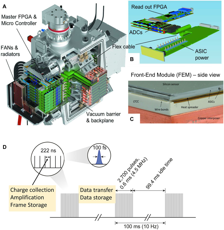
FIGURE 1. (A) CAD model of the AGIPD1M detector with sections cut away to reveal the arrangement of the electronics, both inside and outside of the vacuum vessel (B) The electronics of a single detector module. (C) A photograph of the edge of a Front-End Module (FEM) including annotations of the main components. Figures are sourced from [11]. (D) Pulse structure of the European XFEL and its impact on the requirements for detector data collection.
Each ASIC is composed of a matrix of 64 × 64 pixels; 16 ASICs are bump-bonded to a 512 × 128 pixel silicon sensor, forming the sensitive hybrid assembly unit of the AGIPD detector. This hybrid assembly is then glued to the Low Temperature Co-fired Ceramic (LTCC) board, which is thermally and mechanically connected to the copper interposer, forming the fundamental detector unit - the Front-End Module (FEM). The FEM is connected by means of 500-pin SAMTEC connector to the back-end electronics. A photograph of the edge of a Front-End Module is shown in Figure 1C.
The one-megapixel detector consists of 16 FEMs, grouped into four independently moving quadrants, and is designed to operate in a vacuum environment. Figure 1A shows the CAD model of the AGIPD1M detector with cuts to reveal the arrangement of the electronics both inside and outside the vacuum vessel. From a control point of view, the AGIPD1M detector forms two electronically independent halves (called “wings”). The back-end electronics of each half consist of the ADC boards and the control and data IO board of each module (one set each per module, 8 modules per wing); a vacuum backplane board, which acts as a vacuum barrier and routes signals in and out of the vacuum vessel; a micro controller board for slow control; and a master FPGA board. These boards are located outside the vacuum chamber in a thermally sealed, water-cooled housing. The two master FPGA boards, one for each side, provide the interface to the European XFEL timing system and control the detector FEMs. Another part of the back-end are the boards located in vacuum, they provide power to ASICs and IO signal connectivity between the FEM and the backplane. More details can be found in [11].
Two 1 Megapixel AGIPD detectors are used as primary detectors for experiments at the Single Particles, Clusters, and Biomolecules and Serial Femtosecond Crystallography (SPB/SFX) [3] and Material Imaging and Dynamics (MID) [5] instruments of the European XFEL. The SPB/SFX AGIPD1M system has been installed since the start of operation in 2017, while the MID AGIPD1M followed in November 2018. Both AGIPD1M detectors at the European XFEL are based on the same hardware and firmware, currently using the AGIPD 1.1 ASIC version [16].
It should be mentioned that the second generation of the AGIPD detector is under development and is already in use at the European XFEL as the AGIPD500K prototype, which was installed in September 2020 at the HED Instrument [18]. The AGIPD500K comprises eight modules and is operated in air. This second-generation AGIPD features a new version of electronic boards, new back-end electronics architecture, and uses the new AGIPD1.2 ASIC version [19]. Unlike the AGIPD1M systems, which used complex configurations of several boards with a single function on each, as shown in Figure 1B, the new, more compact readout board incorporates a streamlined design that houses both the analog-to-digital converter (ADC) and a new FPGA, along with all-optical communication via multi-fiber Gbit transceivers. Despite being a prototype, the AGIPD500K detector at HED has been employed in a number of successful user experiments [20, 21] and more are planned.
2 Detector integration and infrastructure
The complexity of integrating a detector into an instrument and the amount of infrastructure required to operate it are illustrated in Figure 2A. The mechanical integration of the detector as well as necessary infrastructure (i.e., cooling, vacuum and powering) was carefully considered to match each instrument’s requests. Furthermore, the detectors have been integrated into the European XFEL control and data acquisition system from a software perspective. The framework of the User Facility generates additional constraints in terms of operability: the detectors are used continuously during long periods (up to 6 days in a row) and run by various teams. Those constraints imply to make the detector setup reliable, secure (interlock systems), maintainable (access to the consumable components) and easy to operate (specific control interfaces), Before being placed at the instrument, the detector was installed in the laboratory for comprehensive testing. This enabled the identification and solving of initial problems and a more efficient installation in the instrument.
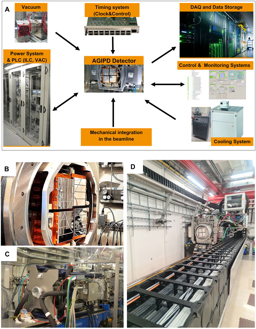
FIGURE 2. (A) Schematic overview of the required infrastructure for AGIPD detector integration. (B) Close-up image of AGIPD1M installation at SPB, showcasing the Front-End Modules (FEMs) in detail. (C) Back view of AGIPD1M installation at SPB, featuring the detector with all cables and pipes connected to the vessel. (D) AGIPD1M installation at MID, with a focus on the drag chain in the foreground, highlighting the detector cables.
2.1 Mechanical integration into the instrument
Both AGIPD1M detectors were required to operate in a vacuum environment. These considerations also factored in the impact of vacuum forces and aimed to ensure the isolation of the detector vacuum from the instrument sample chamber, minimizing the need for frequent system rewarming. Given the multitude of cables required for power, cooling, motors, data acquisition (DAQ), and control, comprehensive support structures were essential. Additionally, accessibility to the Front-End Modules (FEMs) needed to be as straightforward as possible.
Preparation for the mechanical integration of the detector into the beamline began in parallel with detector development. This dual-track approach required adjustments on both fronts to meet the instrument requirements and the needs of the detector development team. The outcome of this integration process is illustrated in Figures 2B–D.
In the current installations, it is relatively straightforward to access the front of the detector, where the FEMs are installed, and this process typically takes only a few hours to 1 day. This is the result of a design decision, since the FEMs are the detector components deemed by far most likely to experience damage–from radiation, by cooling and vacuum accidents, and due to mechanical mishaps. However, gaining access to the rear of the detector poses a significant challenge in terms of both time and the increased risk of damaging critical detector or beamline components. If access to the vacuum boards within the vacuum vessel becomes necessary - for maintenance, repairs or replacements due to malfunctions - a considerable effort is required to access and then open the rear flange of the detector.
2.2 Power system
The AGIPD1M detector electronics is powered by a set of WIENER [22] power supplies, which include Low-Voltage (LV) and High-Current MVP8016 and MVP8008 MPOD multichannel power supplies, providing 16V/5A and 8V/8A power output, respectively. The sensor bias voltage (ranging from 300 to 500 V) is supplied by a High-Voltage (HV) and Low-Current ISEG unit. These power modules are installed and controlled via MPOD crates.
The assignment of MPOD voltage channels (including LV sense) to the detector-head input connectors and cables is carried out near the terminal block, often referred to as patch-panel. Moreover, the terminal block serves the purpose of connecting interlock signals from the power supplies to a PLC (Programmable Logic Controller) and establishing connections for relevant interlock lines between the detector head and the PLC.
In particular, there are no internal DC/DC converters implemented at the detector level in the first generation systems. Instead, each detector board and sensor receive dedicated power from an external power supply. It is worth mentioning that no operational or stability problems have been observed with this power system. The MPOD high-precision supplies meet the electrical requirements (voltage, current, and interlock functionality) of the detectors and can handle the lengths of the cables (30–40 m) used, which is significant. This approach has certain limitations, mainly due to the large number of cables (>100) required to operate AGIPD1M, including 56 power cables, 20 control cables, 16 data cables, and 16 cooling pipes. The thickness of the power cables ranges from 1.5 to 2 cm each, while the cooling lines are composed of pipes ranging from 2 to more than 10 cm in diameter. Therefore, effective cable management and mechanical support are essential when moving the detector within the hutches, as shown in Figure 2D. A more compact design, such as the implementation of DC/DC converters and the reduction of the distance between the detector and dedicated power supplies, would enhance the flexibility of the system and reduce the risk of damaging the detector or power cables during movement.
2.3 Cooling system
The AGIPD1M systems require two cooling circuits: one for the electronics located outside vacuum (with a power consumption of more than 2 kW) and another for the electronics in vacuum (with a power consumption of less than 0.5 kW). For cooling the detector components outside vacuum, we employ a water-based cooling system utilizing commercially available dedicated chillers. No issues have been observed with the cooling of electronics outside vacuum, and the monitored temperatures on the electronic boards remain consistently below 40°C.
Cooling the in-vacuum part of the detector presents considerably greater challenges. In-vacuum electronics are cooled using a customized Julabo water-cooled chiller with silicone oil serving as coolant. The chiller is located in the experiment rack room and requires long (30–40 m) well-insulated cooling pipes to deliver the coolant to the detector cooling blocks. It is essential to note that silicone oil can be difficult to clean and poses a potential hazard to other components of the beamline if it leaks. Fortunately, over the years, no evidence of silicone oil leakage in vacuum has emerged. However, there have been some leaks in the cooling system, particularly in the oil distribution between the chiller and the detector.
The temperature difference between the coolant in the chiller (−32°C) and the temperature of the detector cooling blocks, when no power is applied to the detector head, exceeds 5°C. When the ASICs are active, the temperature of the cooling blocks increases further to above −24°C. FEM temperature measurements, obtained using PT100 sensors installed on the back side of the LTCC board, indicate temperature values ranging from −3°C to +15°C. These readings suggest that the cooling efficiency is limited and that the target temperature (−20°C) cannot be achieved. The gradient between the coolant temperature at the chiller and the attained temperatures on the FEMs is quite substantial, reaching up to 50°C, as illustrated in Figure 3C. The primary cause of the thermal gradient is the limited heat transfer efficiency from the ASICs, which are the main source of heat (approximately 30–40 W per module), in the FEM assembly to the cooling block. The current design, as illustrated in Figure 1C, includes several stacked thermal interfaces, resulting in multiple layers of thermal resistances. Additionally, a large 500-pin connector on the back of the LTCC board hinders heat transfer efficiency, especially in the vacuum environment. Lowering the temperature of the coolant is not feasible, as it can lead to overcooling and malfunction of certain components of the electronic boards installed in the vacuum vessel. Nevertheless, the temperature of the FEMs stabilizes after several minutes and remains constant without fluctuations that could impact the detector characteristics (i.e., the temperature change over time remains below 1°C).
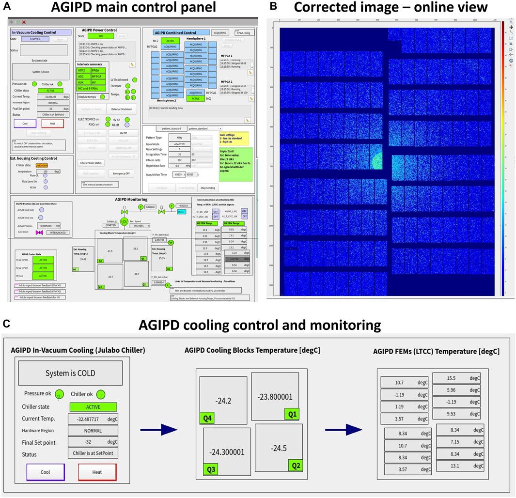
FIGURE 3. (A) Primary AGIPD1M control panel. (B) Illustration of an online-corrected image displayed in the Karabo GUI. (C) Real-time control and monitoring of in-vacuum cooling through the control system, providing temperature information for the cooling blocks and Front-End Modules (FEMs).
To address this problem in the next-generation of detectors, a dedicated R&D program has been initiated. The goal is to explore more efficient cooling methods, such as micro-channel cooling [23], to enhance overall cooling performance. The advantage of this cooling method lies in the positioning of micro-channels directly under the readout ASICs, optimizing heat dissipation.
2.4 Interlock system for detector protection
The interlock system for the AGIPD1M detectors is based mainly on programmable logic controllers (PLCs) [24]. These PLCs monitor the vacuum quality and cooling efficiency, reading out temperatures of the detector cooling blocks; pressure values from the sensors installed at the detector vessel and in the connected sample chamber; chiller conditions; and internal detector conditions evaluated by the detector slow-control board, such as hardware conditions and temperatures of the FEMs. If necessary, the PLCs take appropriate actions. The interlock logic implemented for the AGIPD1M detectors is shown in Table 1.
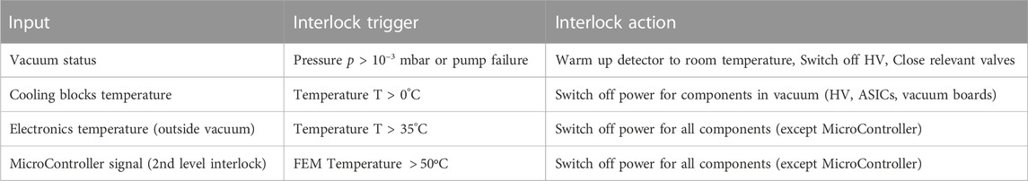
TABLE 1. Interlock triggers and actions.
Over several years of practical experience, this system has proven to be highly effective in protecting the detector against unexpected failures, such as pump or chiller failures, power outages, or inadvertent cooling shutdowns. This level of protection is absolutely indispensable for smooth detector operation within a user facility like the European XFEL. Ideally, the detector system has to possess self-protective capabilities.
Another category of incidents refers to radiation damage resulting from the primary or scattered/diffracted beam. Such incidents can occur, and components primarily affected by radiation, such as ASICs and sensors, should be explicitly designed to be radiation-hard, as protecting them from such events is generally challenging. In most cases, radiation damage is caused by high-intensity X-ray radiation generated in a single shot, which leaves no time to react. However, there is a class of incidents that can be prevented or significantly minimized. An example is the formation of ice on the sample injection nozzle. This can be monitored, and if ice is observed, the beam must be attenuated or the shutter must be closed. Such a protection system has recently been developed and is planned to be used at the SPB/SFX instrument.
2.5 Control and monitoring system for AGIPD1M
The control system for the AGIPD1M detector, together with its associated infrastructure including power supplies, cooling and interlock systems, has been integrated into the European XFEL control framework known as Karabo [25]. Its core relies on transparently distributable servers, offering functionality through pluggable “devices”. These devices can function as control interfaces for tasks such as motor control or detector control, monitoring interfaces for measurements such as pressure readings, or computational devices for data processing.
Karabo also supports complex procedures, such as detector startup, by employing “middle-layer devices”. These devices do not directly interact with hardware but instead coordinate with other control devices, consolidate incoming data, and execute the necessary steps. These high-level interfaces enable detector operators, including instrument scientists, to efficiently manage these systems independently. In addition, they serve as a second-level safety mechanism which will not allow to perform actions that can be dangerous for the detector hardware (i.e., powering the detector when the temperatures or pressure are not in the expected range). These interfaces facilitate various tasks, including power management, configuration adjustments, and the efficient acquisition of calibration data needed for the production of calibration constants used for raw data corrections. As an example, Figure 3A displays the AGIPD main control panel, while Figure 3B presents an online-corrected image.
Interactivity is provided through either a command line interface (CLI) using IPython with automatic command completion or a PyQt-based graphical user interface (GUI). The GUI consolidates parameters, control and data flows, state information, and error feedback, enabling the creation of complex control and processing configurations, including data analysis pipelines such as the data correction pipeline.
Any newly developed operational features undergo rigorous integration and testing procedures before being deployed for user operations. Consequently, the control system for the AGIPD1M detectors demonstrates impressive stability and is free of significant issues or instabilities.
2.6 Data collection and storage infrastructure
Acquiring meaningful data from the detector requires precise synchronization with the European XFEL beam, a feature accomplished through the Clock and Control (C&C) system [26]. This system plays a crucial role in ensuring synchronization by providing essential components such as clocks, bunch, and train-related information. Importantly, the C&C system can also issue veto signals to discard undesirable bunches, although it is pertinent to mention that AGIPD currently does not employ this functionality. The information from the C&C system is first received by the AGIPD1M Master FPGA (MFPGA), and then is distributed to all detector modules. Following this, raw data from the detector, including the train Id information, is transmitted via the UDP protocol to the European XFEL Data Acquisition PC Layer and written in HDF5 data format [27]. Initially, this data is stored within the online GPFS (General Parallel File System) [28] cluster, while the metadata is concurrently made accessible through the metadata catalogue myMdC [29]. myMdC offers the ability to evaluate the data before copying it from the online cluster to the offline GPFS cluster. Moreover, in addition to the raw data, the corrected data, referred to as “processed data,” is also retained.
3 Data quality: characterization and calibration
3.1 Calibration strategy
Accurate calibration and comprehensive characterization of detectors are critical aspects to ensure the successful operation of instruments employing these detectors. Equally important is the development of user-friendly procedures and tools that facilitate recalibration during the operational phase. In this section, the general concept of AGIPD calibration, shown in Figure 4, is explored, and a more detailed explanation of the calibration process is provided.
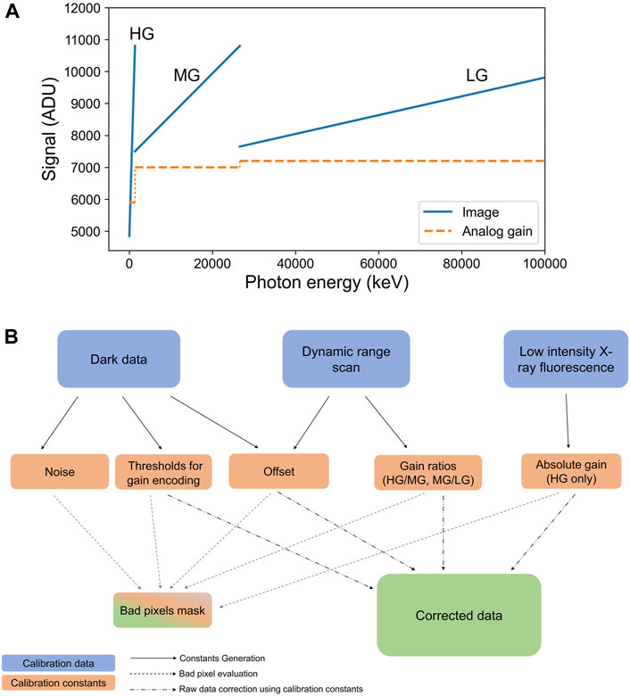
FIGURE 4. (A) Visualization of AGIPD’s dynamic range, showcasing three adaptive gain settings: High Gain (HG), Medium Gain, and Low Gain (LG). (B) Flowchart illustrating AGIPD’s calibration strategy.
To fully calibrate the AGIPD detector, three distinct data sets are required:
1. Dark data (without any external stimulus) to determine offset and noise values for each gain setting and two thresholds for gain encoding.
2. Dynamic range scan of available gain settings with internal calibration sources to provide ratios between different gain settings as well as offsets for each gain.
3. Low-intensity fluorescence data are used to determine the absolute gain value.
All three gain settings, as illustrated in Figure 4A, require characterization for each memory cell within each pixel. This characterization involves 11 parameters, including:
1. Three offsets, one for each gain setting.
2. Two thresholds for gain setting encoding.
3. One absolute gain value.
4. Two gain ratios: HG/MG and HG/LG.
5. Three bad pixel maps for each gain setting using information from the data sets mentioned above, and it is kept as a 32 bit mask to prevent the source of the bad pixel from being lost.
This results in more than 4 × 10⁹ unique parameter values for an AGIPD1M detector. The calibration constant values strongly depend on the operating mode, including also factors such as acquisition rate, the number of memory cells used, and integration time. Therefore, each operational scenario requires dedicated calibration data collection and analysis to derive calibration constants tailored to that specific operating mode. The constants are generated using a dedicated calibration software, which is run on the Maxwell - HPC cluster [30] at DESY. Table 2 shows the estimated time needed for the collection and processing of the calibration data to obtain a complete set of calibration constants for the AGIPD1M detector and one operation mode. It also includes how frequently the constants are generated for each of the operation modes. Multiple detector operation modes were implemented to enhance detector performance for specific types of experiments and address observed problems, as detailed in Section 4.
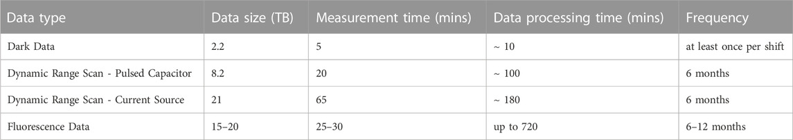
TABLE 2. Summary of data collection and processing times and sizes, as well as frequency of generation for one complete set of calibration constants for the AGIPD1M detector at the European XFEL. The presented values are based on the operation mode with all memory cells and do not include preparatory time required for the measurements.
The generated constants are injected into the calibration database [31] and automatically retrieved to correct the raw data [32]. It is quite a challenging process because of the amount of data that has to be collected and processed to generate the full set of calibration constants. Another challenge is caused by detector artifacts, which require additional data treatment, as described in more detail in Section 4.2.
3.2 Detector baseline
The detector baseline (offset) is defined as a dark signal measured in the absence of external stimuli, such as X-ray photons. In the ideal scenario, the baseline measured under well-defined conditions (e.g., temperature, readout speed, integration time) should enable the subtraction of signals not originating from incoming photons. It should also be independent of the intensity value and remain stable over time.
The dark data is acquired using a dedicated configuration, which allows the detector to be forced into Medium or Low gain settings. The collected data is then processed, and the new versions of constants (offsets and noise maps) that are generated can be used for data correction. The offset O) is calculated as the median of the dark signal (Ds) over a certain number of trains t) for a given gain setting (gs: 0-HG, 1-MG, 2-LG), pixel (x, y) and memory cell c). The noise N is calculated as the standard deviation σ of the dark signal
The calibration constants from dark data are generated on a regular basis (i.e., at least once a day during user experiments). To ensure the frequent generation of the constants, the acquisition and processing of dark data is automated, facilitating the task for the beamline operator.
3.3 Gain setting identification
As mentioned in Section 1.2, the beam’s time structure at the European XFEL does not allow for a continuous readout of single frames during pulse trains. Therefore, each frame in the train, up to a maximum of 352, must be stored in pixel and is read out in the 99.4 ms gap between pulse trains. Since both the information regarding the pulse height of the charge-integrated signal and the gain status are essential for extracting incident X-ray intensities on the detector, each AGIPD pixel has two storage cell matrices, each consisting of 352 capacitors. One matrix stores analog information about the height of the X-ray signal, and the second one stores the signal related to the gain setting (i.e., V = 0.7 V for HG, 1 V for MG and 1.5 V for LG) that is being used (Ig).
The dark data is used not only for noise and offset determination, but also for generation of constants that are needed for the identification of gain settings, so-called thresholds. Analog gain levels (Gi) for each gain setting (where i = HG, MG, and LG) are calculated as the median of the dark gain signal (median (Dgs)) over a certain number of trains t) for a given gain setting (gs: 0-HG, 1-MG, 2-LG), pixel (x, y) and memory cell c). The noise associated with the gain level is quantified as the standard deviation of
• High gain if Ig ≤ T0
• Medium gain if T0 < Ig ≤ T1
• Low gain if Ig > T1
Where the thresholds T0 and T1 are determined as the mean value between individual analog gain levels (Gi), that is,
The original idea was to use two thresholds per chip (64 × 64 pixels) since the three gain values were expected to be well-separated and have similar values for each pixel and memory cell. A study [16] carried out on a single AGIPD1.1 ASIC in a dedicated test system showed that up to 0.5% of pixels can have an incorrect gain assignment if only two threshold values are applied per chip. Analysis of data collected with the full-scale system (AGIPD1M at the European XFEL) revealed that applying ‘sanity cuts’ to filter out outlier values of analog gain (i.e., selecting gain values within ±5 standard deviations from the average gain value for all pixels and memory cells) resulted in the removal of at least 0.5% of the pixels. Analog gain values for medium and low gain in a single ASIC overlap, as shown in Figure 5A. Therefore, using only two thresholds per chip is not feasible if we want to maintain a sufficiently low probability of ‘false’ encoding (preferably below 0.1%). Studies show that the gain separation MG-LG strongly decreases for pixels close to the chip periphery (Figure 5B) and exhibits a strong temperature dependency, pointing towards a leakage current. Another observed issue, as shown in Figure 5C, is that the difference in the gain level value for medium and low gain degrades along the memory cell’s number in the read-out sequence, and it is not always possible to determine if the signal is collected at medium or low gain.
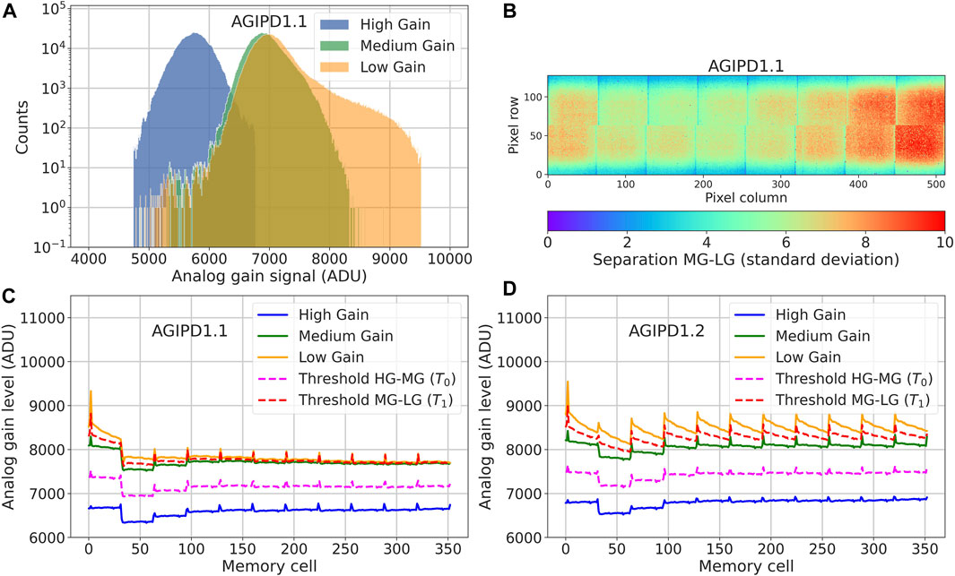
FIGURE 5. (A) An example of analog gain signal (Ig) values for each pixel and memory cell in a single AGIPD1.1 ASIC. (B) Average separation between MG and LG across all memory cells in a FEM equipped with AGIPD1.1 ASICs. Separation is defined in units of analog gain level noise values
The observed effect is caused by a bug in the chip design, which, during the data readout of the 352 image and 352 gain memory cells, results in a partial discharge of the gain signal in a particular gain memory cell if the encoded gain level stored in that cell corresponded to LG. As gain cells are read out sequentially from cell0 to cell351, the cells that are read out later have already been deprived of a significant amount of charge if they are in LG, causing their voltage levels to reduce to levels encoding MG. Therefore, for cells read out later, no MG-LG distinction would be possible anymore, even if individual thresholds are applied to each memory cell in each pixel. A new version 1.2 of the AGIPD ASIC mitigates this issue (Figure 5D). However, both AGIPD1M systems at the European XFEL are currently equipped with the AGIPD1.1 ASIC version. Therefore, low gain is not used for scientific analyses and is still not fully characterized. The installation of FEMs equipped with AGIPD1.2 ASICs is planned in the near future.
3.4 Dynamic range
To establish a relationship between different gain settings and effectively calibrate the entire gain of the detector, it is essential to perform an intensity scan throughout the entire dynamic range of the detector. However, using the European XFEL beam, conducting a comprehensive intensity scan for every memory in every pixel within the entire dynamic range proved to be unfeasible. Therefore, X-ray photons are exclusively used to determine absolute gain factors in HG, as is elaborated in Section 3.5.
To perform a dynamic range scan of the detector, we rely on the available internal “on-chip” calibration sources. Alternative methods, as described in [33], such as dynamic range scans with sensor backside pulsing, IR pulsed laser, pulsed monoenergetic proton beams, or LED light, are not viable for the full-scale AGIPD1M system for several reasons. Primary factors include the need for specialized installations and interfaces to the ASICs, which are absent in AGIPD1M and would require a complete disassembly of the detector to execute the scan. Some of these methods are suited only for single-pixel scans, for example, the laser and pulsed monoenergetic proton beam, which are not applicable to the detector module or system. Therefore, in our specific case, we rely on the internal calibration sources implemented at the ASIC level.
The AGIPD detector provides two options for injecting test charges into pixels. One approach for scanning the dynamic range involves employing the Pulsed Capacitor (PC), a circuity implemented at the input of the preamplifier of each pixel, which allows for applying voltage steps to a capacitor to introduce a defined, albeit small, charge. The second approach utilizes an on-chip current source (CS), which permits the injection of a constant current into the preamplifier’s input. By increasing the integration time, the amount of charge injected will increase in proportion, allowing for a thorough scan of the detector’s dynamic range. The current source implemented on the AGIPD ASIC is programmable, allowing its current value to be tailored to specific ASIC instances to encompass the entire dynamic range.
At the European XFEL, we primarily utilize the PC source for calibration purposes. The CS source is also implemented, and the first set of calibration constants has been generated. However, the application of LG in the current version of AGIPD1M is restricted due to the issue mentioned in Section 3.3. Consequently, the full characterization and validation of this internal calibration source remains a work in progress. To prepare the calibration, we first scan the dynamic range by injecting test charges into the pixels. The calibration process then involves two steps. First, we subtract offsets derived from the dark data from the scan data. Next, we model the data distribution using a fitting method to determine the relationship between different gain settings. An example of a dynamic range scan with Pulsed Capacitor is shown in Figure 6A.
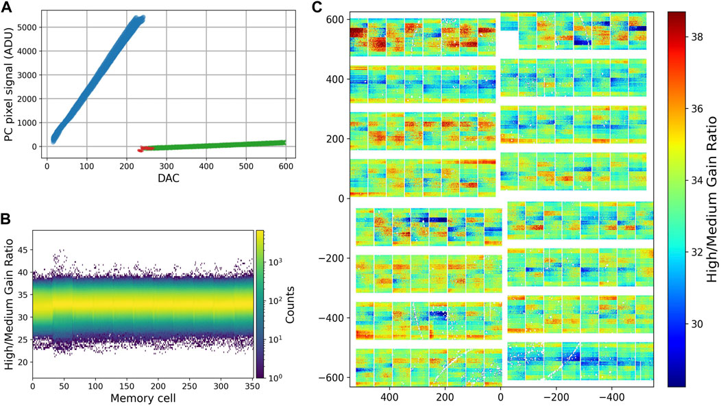
FIGURE 6. (A) Dynamic range scan example using the Pulsed Capacitor (PC). The blue region corresponds to the high gain setting, red represents the transition region between the high and medium gain, and green represents the medium gain region. (B) High gain to medium gain ratio values for all pixels of a single module, plotted as a function of the memory cell index. (C) High gain to medium gain ratio map for AGIPD1M, averaged across all memory cells.
For the initial part of the distribution, a linear function is fitted to the data, allowing us to establish the gain slope and offset for high gain settings, expressed as y = mx + l. For the subsequent regions, we employ a composite function: y = A ⋅e−(x−O)/C + mx + l, which enables us to cover both the transition region and the medium gain slope and offset. However, due to the inherent challenges posed by the transition region between high and medium gain settings, as discussed in more detail in Section 4.2.2, and the difficulty in reliably applying these models for the correction of detector data (since distinguishing between pixels in the transition region and valid MG values can be challenging), we opted to exclude from the analysis the scan intensities corresponding to the transition region. Instead, we fit only the linear part of this function to generate the calibration constants. The results of the analysis are presented in Figures 6B, C. In Figure 6B, the gain ratio values for all pixels in a single AGIPD FEM module are shown as a function of memory cell index. Figure 6C shows the average gain ratio (HG/MG) map for AGIPD1M at SPB/SFX, computed across all memory cells.
The procedure for obtaining calibration constants from the dynamic range scan data collected with CS is similar. In this case, we fit three linear functions to each gain region and derive the gain setting ratio from the slopes of the fit.
It is important to note that while both sources are valuable tools, they do come with limitations: the PC source can cover only HG and a relatively small part of MG, typically around 10%, primarily up to a few hundred 10 keV photons. On the other hand, CS spans all gain settings, but is not compatible with the European XFEL timing. In both cases, certain artifacts may be visible in the data that are not always reproducible when collecting X-rays.
3.5 Absolute gain conversion factors from low intensity fluorescence data
The absolute calibration in the high gain (HG) region, quantified in terms of the conversion factor ADU/keV, is executed using low-intensity, flat-field fluorescence photon data. These measurements are conducted right at the beamline, eliminating the need to disassemble the detector system from the instrument. Typically, a copper (Cu) foil serves as the medium for these measurements, although at higher energies, such as with Yttrium Y), the measurements are adapted accordingly. To prevent rapid degradation of the material under the intense XFEL beam, the X-ray beam size on the foil is intentionally defocused to approximately 100 μm × 100 μm. Additionally, the intensity of the incident X-ray beam is finely tuned to yield a detectable signal of around half a photon per pixel per pulse. The distance between the detector and the interaction point is adjusted to ensure uniform illumination of the entire detector simultaneously. This uniformity can be achieved at distances on the order of 100 cm and beyond.
The collected data (approximately 15,000 events for each memory cell in every pixel) after offset subtraction is used to determine the absolute gain factors. This determination is made by evaluating the separation between the photon peak positions, including the 0-photon (noise) peak. The position of these peaks is derived by fitting a multi-Gaussian function to the single-photon spectral distributions collected for each memory cell within each pixel, as shown in Figure 7A. This process involves performing a total of 352 million fits for AGIPD1M. Figure 7B shows the absolute gain factors for high gain as a function of the memory cell index for one of the FEM modules installed in AGIPD1M at SPB/SFX. Additionally, an example of an absolute gain map for high gain, averaged across all memory cells in a pixel, is presented in Figure 7C.
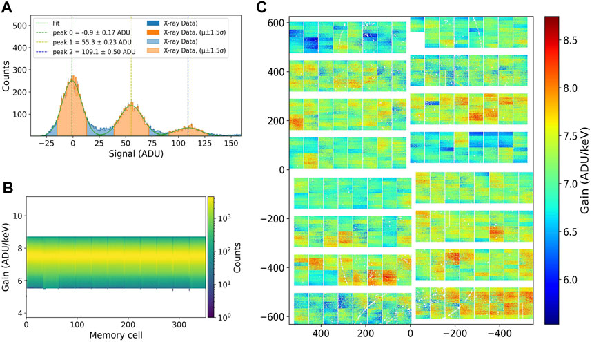
FIGURE 7. (A) An example of low-intensity Cu fluorescence (Eγ = 8.05 keV) spectrum for single pixel and memory cell. Multi-Gaussian function was fitted to the data. (B) Absolute gain values of high gain setting as a function of memory cell index for one of FEMs installed in AGIPD1M detector at SPB/SFX. (C) Absolute gain map of high gain setting for AGIPD1M installed at SPB/SFX, averaged across all memory cells.
The absolute gain values, in conjunction with the gain ratios obtained from the dynamic range scans described in Section 3.4, provide a comprehensive calibration of the detector gain.
3.6 Bad pixels determination
The accurate identification and classification of all detector channels, in this case pixels, is essential for any scientific analysis. This process involves recognizing and documenting information regarding pixels that do not perform optimally. The primary objective of this identification is to facilitate the exclusion of problematic pixels from the analysis. This information is encapsulated within what is commonly referred to as a “bad pixel mask”.
Problematic pixels can exhibit various issues. Some may be non-functional, a condition commonly referred to as “dead pixels.” Others may not respond to X-ray stimuli, exhibit excessive noise, or display parameter values outside the expected range.
The identification of these problematic pixels is based on the evaluation of calibration constants derived from the calibration data mentioned above and provided to users with the corrected data.
1. As an initial step, detection of abnormal or “dead” pixels involves evaluation of the offset and noise values derived from dark data. A pixel is flagged as “bad” if one of these values exceeds or falls below predefined thresholds. Two threshold settings are available: one establishing absolute limits for noise and offset values and the other determined by the standard deviation calculated from mean offset and noise values across all memory cells and pixels. Typically, pixels with values exceeding ±5 standard deviations from the mean are classified as “bad pixels.” These threshold settings are adjustable, allowing for more leniency or stringency depending on the specific requirements of the scientific analysis. For example, when dealing with sparse XPCS data, a more conservative definition of “bad pixels” may be necessary to minimize the detection of “false positive” single photons.
2. Identifying pixels that might exhibit normal behavior in high gain but struggle to transition to medium or low gain settings is the next step. To recognize these problematic pixels, internal charge injection data is used. Pixels are classified as ‘bad’ if their gain ratios exceed or fall below predefined thresholds, which are determined in the same manner as for offset and noise values derived from dark data.
3. The final refinement of problematic pixel detection is achieved using data obtained with X-rays. These data allow for the identification of pixels that are insensitive to X-rays and pixels with abnormal absolute gain values that exceed predefined thresholds, which are defined in the same manner as previously described for other calibration constants.
4 Operational aspects–performance and reliability of AGIPD detectors
4.1 Scientific outcome
The AGIPD detector is used in different kinds of experiments. The following sections give an overview of the main experimental techniques used with AGIPD and highlight some of the published results.
4.1.1 Serial femtosecond crystallography
High peak brilliance, combined with the MHz repetition rate of X-ray pulses, makes the European XFEL exceptionally attractive for serial femtosecond crystallography (SFX), a method routinely used to study both the structure and dynamics of proteins at room temperature [34]. SFX employs the “diffract before destruction” principle. This means that, due to the short duration of the incident X-ray pulses, a diffraction signal is collected before the sample is obliterated by the X-rays. The SPB/SFX instrument at the European XFEL is purpose-built to facilitate these SFX-type measurements. The AGIPD1M detector is an integral component of the in-vacuum interaction region at SPB/SFX and among its crucial attributes for SFX are the high dynamic range and MHz acquisition rate. In a typical experiment, sub-micron crystals suspended in a low-viscosity buffer medium are injected into the X-ray beam in the form of a liquid jet. Resolving a protein structure requires around ten thousand randomly oriented diffraction patterns. Taking into account an average crystal hit rate of approximately 1%, this requires the collection of approximately a million images in the shortest possible time frame. The high repetition rate of X-ray pulses at the European XFEL allows the recording of diffraction data more than an order of magnitude faster than previously achievable [35]. The most common configurations are 3,510 images per second at a detector acquisition rate of 1.13 MHz or approximately 2000 images per second at a detector acquisition rate of 0.56 MHz. The reason for collecting fewer images at 0.56 MHz compared to 1.13 MHz is due to the constraints on the number of pulses available from the XFEL accelerator at this repetition rate. Specifically, the RF window is limited to a maximum duration of 600 µs, and these pulses are distributed among three beamlines simultaneously. An example of an experimental setup used for SFX is provided in Figure 8A, while Figure 8B presents a single-crystal diffraction image captured with the AGIPD1M [37]. Multiple experiments have convincingly demonstrated that data recorded with the AGIPD1M and calibrated with the European XFEL calibration routine yield high-quality results [36, 41, 42].
FIGURE 8. (A) Experimental setup for SFX measurements (originally published in [36]). (B) Example serial crystallography data taken using AGIPD1M during early user experiments at SPB/SFX. Note the well-defined Bragg peaks that span a large fraction of the detector dynamic range (published in [37]). (C) Experimental setup for SPI experiments (originally published [38]). (D) Examples of scattering patterns from IrCl3 and Mimivirus recorded by AGIPD1M (originally published in [39]). (E) Experimental setup for XPCS experiments published in [40]). (F) Example of the mean scattering intensity of an aqueous silica nanoparticle solution recorded by AGIPD1M (originally published in [5]).
4.1.2 Single particle imaging
Single particle imaging (SPI) is a technique oriented towards resolving the structure of individual particles or molecules based on a multitude of interactions between X-ray pulses and the sample. The underlying principle of this experiment is illustrated in Figure 8C. The SPI technique uses high repetition-rate X-ray pulses provided by the European XFEL to capture 2D diffraction patterns from a repeatable sample in random orientations. It relies on statistical sampling to gather diffraction patterns, which are subsequently analytically combined to reconstruct the 3D electron density of the sample. In the case of SPI, low noise and the capability to resolve a single photon are among the key requirements for the detector. In practice, tens of thousands of good quality patterns are necessary to complete the measurement. During SPI experiments, the AGIPD1M typically operates at its highest frame rate. For investigations involving weakly scattering samples, AGIPD offers the flexibility to adjust the gain of the Correlated Double Sampling (CDS) stage [15] of the pixels. This adjustment enhances single-photon resolution at the cost of reduced dynamic range.
The AGIPD1M detector has demonstrated performance, allowing the successful execution of single particle imaging experiments at SPB/SFX. Detailed results from a study on gold nanoparticles are presented in [38], while the findings of studies involving Iridium Chloride (IrCl3) and Mimivirus are presented in [39]. Examples of scattering patterns from these experiments are shown in Figure 8D.
4.1.3 X-ray photon correlation spectroscopy
X-ray Photon Correlation Spectroscopy (XPCS) is a technique used to investigate the dynamics and kinetics in hard and soft condensed matter samples. At synchrotrons, it conventionally enables the probing of dynamics at timescales ranging from milliseconds to hours. However, the MHz repetition rate of the European XFEL and the AGIPD detector permits exploration of structural dynamics at much shorter timescales, in the sub-microsecond range. This is particularly relevant since sub-microsecond and microsecond timescales are natural for the diffusion of biophysical systems and nanoparticles in their aqueous environments [40]. An illustration of an XPCS experiment and the average scattering intensity obtained from the analysis of the data collected with the AGIPD1M detector are shown in Figures 8E, F respectively.
XPCS exploits the coherence of the XFEL beam, by recording speckle patterns of typically non-crystalline samples, which encode the spatial arrangement of the scatterer. The dynamics can be obtained from a series of such speckle patterns by calculating the temporal auto-correlation function. The AGIPD was designed primarily for experiments such as imaging or femtosecond crystallography. However, it can also be utilized for X-ray Photon Correlation Spectroscopy (XPCS) under certain conditions. One main challenge is to detect the speckle pattern with sufficient spatial resolution. The speckle visibility (or speckle contrast in XPCS experiments) is diminished if the pixel size of the detector is large compared to the speckle size, with an optimum Signal-to-Noise ratio if both quantities are equal. In user experiments probing nanometer length scales in small-angle (SAXS) configuration this criterion can readily be achieved by sufficient focusing of the X-ray beam. Several user publications have used this configuration successfully and it is offered as standard configuration at the MID instrument [5]. Early exploratory studies [5, 43–45] were built on a previous experiment at SPB/SFX [40], and have since been followed by more application-oriented experiments on protein aggregation and diffusion [46], functional nanoparticle self-assembly, or temperature-jump swelling-deswelling kinetics of PNIPAM nanogels [47].
Extending these measurements to atomic length scales in wide-angle (WAXS) geometry has proven to be more challenging. The finite longitudinal coherence length leads to a further reduction of speckle contrast in addition to the one due to the large detector pixels. Additionally, the scattering intensity at larger angles is typically much reduced, making it comparable to the inherent noise level of the detector. To accommodate the sources of noise in AGIPD that can negatively impact XPCS data analysis even at higher intensities, a special data treatment had to be developed, as reported later in 4.3. This has proven to work well for most of the XPCS experiments in SAXS geometry; however, for WAXS experiments the noise characteristics at lower intensities as well as the large pixel size at smaller speckle contrasts remain challenging.
4.2 Performance challenges and continuous improvements
The data obtained with all AGIPD detectors installed at the European XFEL have been used to generate a considerable amount of scientific output. More than 20 publications have been produced on the basis of the data collected with these detectors. The experience with the commissioning, calibration and operation of the AGIPD has allowed us to identify several shortcomings that affected the quality of the data. The European XFEL and AGIPD Consortium have made a significant effort to understand the behavior of the detector and to successfully improve its performance. This involved hardware enhancements, optimization of detector configurations, and software data processing that are described in the following sections.
4.2.1 Baseline shift dependence of incoming X-ray intensities
It was observed that certain pixels in the images exhibit negative intensity values, and this effect becomes more pronounced as the overall intensity in this FEM module increases. To quantify this effect, a ‘mask’ was installed in front of the AGIPD1M detector at SPB/SFX, shadowing some parts of all FEMs, and an intensity scan was performed. An example image is shown in Figure 9A. This data was further analyzed and yielded the following observation: the common baseline signal of a module shifts to lower values, and the shift is linearly proportional to the incoming X-ray intensity causing a ≈20% decrease in the level of measured photon signal.
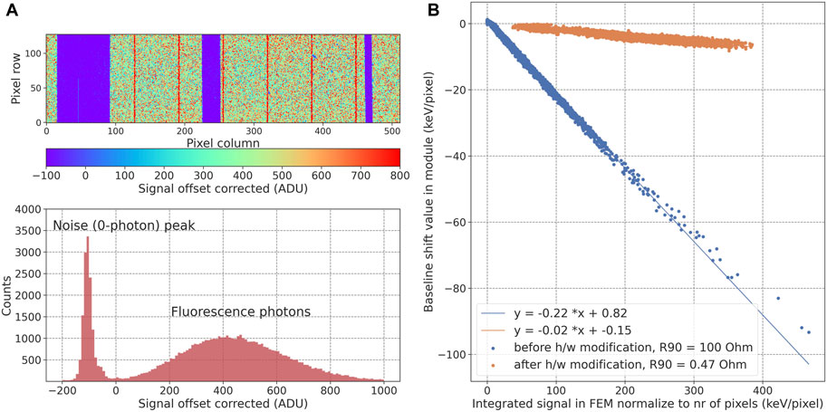
FIGURE 9. (A) A single image illuminated with high-intensity Cu fluorescence photons after offset subtraction. The three areas in purple color represent the part of the module covered with Ta stripes. The histogram illustrates the shift of the noise peak toward negative values resulting from the baseline shift. (B) Baseline shift value as a function of the integrated signal in FEM, normalized to the number of pixels, before modification of the vacuum board hardware (depicted in blue) and after modification of the hardware (depicted in orange). Linear functions were fitted to each dataset to quantify the baseline shift effect before and after hardware modification, resulting in an order of magnitude reduction of the effect.
The issue is caused by the depletion of the sensor, which then also acts as a capacitance, and the resistor connecting it to the high-voltage (HV) input, in this case exacerbated by the parallel capacitances of a Pi-filter. The purpose of a resistor at this point is to limit the current, once the HV has to be turned off. This current limitation also affects sensor signals: Once the sensor absorbs X-rays, it cannot be re-charged immediately due to the finite RC − time constant, and in turn the high voltage drops by a finite amount, registered as a shifted baseline.
These resistors were exchanged on all AGIPD1M vacuum boards, leading to a reduction in the baseline shift to <2% of the deposited signal. The baseline shift before and after hardware modification is plotted as a function of the integrated intensity in Figure 9B. This effect is most pronounced for pixels in high gain as the aforementioned resistors are in series with the input impedance of the preamplifier. Since the latter is reduced by switching to MG or LG, the RC − time constant is further lowered, and consequently the baseline shift is further suppressed.
4.2.2 Gain continuity close to the transition region
In scattering experiments, the presence of randomly fluctuating pixels exhibiting unusually high signal values, commonly referred to as “snowy pixels”, was observed. These snowy pixels tend to manifest when incident X-ray intensities approach the transition region between high and medium gain stages. Although the gain setting of these pixels is classified as medium gain based on their analog gain signals, a closer examination reveals that the signal levels of these pixels do not align with expected intensities. They appear to exhibit values that are inadequately low for high gain and excessively high in medium gain settings. An example of snowy pixels is shown in Figure 10A. These pixels, depending on context, may look like valid events, e.g., in a Bragg peak, and actually disturb analysis.
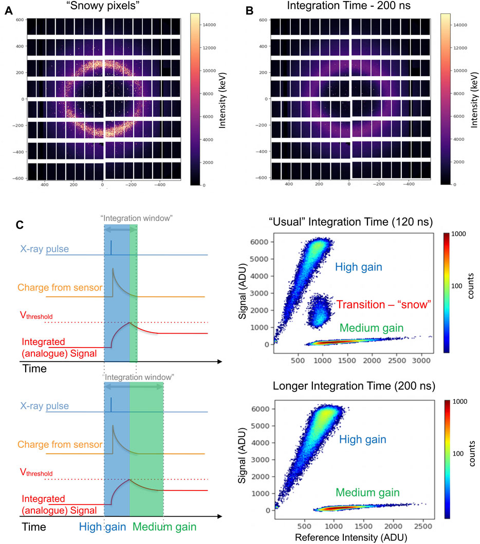
FIGURE 10. (A) Image of a water jet ring collected with the AGIPD1M detector at SPB/SFX with a 120 ns integration time. Snowy pixels are identified as those with unexpected high-intensity values. (B) Image of a water jet ring taken with the AGIPD1M detector using a 200 ns integration time. The presence of snowy pixels is to a large extent suppressed. (C) Illustration of the late gain switching mechanism (left plot) and intensity scans for a single pixel (right plot), including the transition region between high and medium gain visible for the integration time of 120 ns.
The appearance of “snowy pixels” within the detector can be attributed to a late gain switching effect. In the AGIPD system, a voltage representing the collected charge is written to the analog memory at the end of the integration time. However, when gain switching occurs too close to the end of this period, the CDS stage, which has the lowest bandwidth in the ASIC, does not have enough time to settle, resulting in an excessively high stored voltage. Late gain switching can be influenced by several factors. One is the relatively short integration time, despite the XFEL pulses being extremely short, i.e., tens of fs. The charge collection time for the sensor is several tens of nanoseconds, and the profile of this charge collection approximates a falling exponential curve. Consequently, the tail of the signal charge may overlap with the end of the integration time, potentially causing incomplete stabilization of the signal before integration is completed, as illustrated in Figure 10C. Furthermore, noise can be a contributing factor, as random noise can trigger gain switching for signals near the threshold. Additionally, the leakage current becomes relevant for signal levels close to the threshold, which eventually leads to gain switching.
To mitigate the issue of “snowy pixels,” two potential solutions have been identified that do not require a re-design of the ASIC. Both solutions aim to optimize the detector configuration to enhance the quality of output data for specific experimental methods. In situations where ensuring single-photon sensitivity is crucial while maintaining a high dynamic range, and considering that most experiments at SPB/SFX and MID typically involve pulses at repetition rates below 4.5 MHz (i.e., 2.25 MHz or lower), extending the integration time is an option to consider. In this mode, the pulse is recorded at the beginning of the integration window and the window itself is prolonged. Operation of the detector with an extended integration time results in a substantial reduction in snowy pixels, reducing their occurrence from around 10% to below 0.01% for transition region intensities. This improvement was verified through a dedicated measurement at the SPB/SFX instrument, specifically with water jet scattering and two integration times of 120 ns and 200 ns. A comparison of the results is shown in Figures 10A, B, which highlights the significant improvement in data quality when integrating over 200 ns. On the other hand, if single-photon sensitivity is not required, the AGIPD can be operated in a fixed medium gain mode, where the detector gain is set to a predefined value (i.e., medium gain), and dynamic gain switching is disabled. This approach prevents transitions between gain stages. However, it is not suitable for low-intensity data that require single-photon sensitivity, as it leads to increased noise from approximately 1.3 keV to more than 40 keV.
4.3 Dealing with very sparse data
In experiments with low photon intensities, particularly when dealing with sparse data (i.e., below 0.1 photon per pixel per pulse), a special operation mode is implemented to minimize noise and increase the single-photon sensitivity. This mode effectively reduces noise levels from 1.3 keV to approximately 0.9 keV, resulting in a narrower dynamic range limited to only a few tens of photons. This operation mode has become the standard mode of choice of SPI 4.1.2, XPCS 4.1.3, or fluorescence correlation imaging [48].
In addition to the standard correction using calibration constants, specific common-mode corrections are additionally applied. Common-mode noise denotes a type of signal variation that affects groups of read-out channels in a synchronized manner. It can arise from various sources, including common electromagnetic interference or voltage fluctuations. Common-mode noise not only contributes to overall noise levels, but can also potentially introduce artificial hit patterns. The extent of its impact varies depending on specific detector components, such as ASICs, and the surrounding environmental conditions. The precise spectrum of common-mode noise is typically not known in advance. In certain cases, the contribution of common-mode noise can be estimated either on a per-image basis or for groups of read-out channels. This process involves subtracting the offset from the raw signals, excluding the channels with the actual signal, and computing the average signal observed on these channels. This calculated average signal provides a reasonable estimate of the contribution of common-mode noise, which can then be subtracted from the signals.
For the AGIPD1M detectors, two sources of common-mode noise have been identified: one at the ASIC level and another along the memory cell rows (due to the cells being grouped into 11 × 32 matrices, as described in Section 1.2). Correcting for common-mode noise significantly improves data quality, especially when dealing with sparse intensities, as demonstrated in Figure 11. However, it is essential to note that common-mode corrections may not fully address all issues related to offset instabilities. In specific instances, it has been observed that a small fraction of pixels (less than 0.01%) experience “jumps” in offsets within blocks of 32 storage cells, but for several consecutive trains. While the magnitude of these “jumps” is typically on the order of a single photon, synchronous jumping of several storage cells in one pixel can introduce significant artifacts in correlation analyses, such as XPCS where different storage cells are correlated with each other. To address these issues, a tailored correction approach becomes necessary as part of data analysis. As an example, the corrections to mitigate the ‘jumping’ pixel issue were developed by MID and the XPCS user community and were successfully used during data analysis [5, 43]. This method involves calculating not only the temporal autocorrelation function within one train (along the storage cell dimension) but also cross-correlation terms involving data from different trains. Since the measured speckle pattern should be uncorrelated from train to train, the resulting correlation matrices should primarily contain terms originating from jumping-pixel contributions. This approach has been shown to mitigate this artifact down to low intensities of 10–2 − 10–1 photons per pixel per pulse, but was not sufficient to correct XPCS data at even lower intensities.
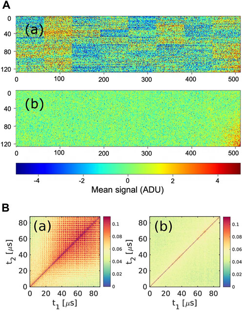
FIGURE 11. (A) Example of common mode corrections effect on low-intensity data: mean intensity over 100 trains without common mode corrections (a) and with common mode corrections (b). (B) The two-time correlation function: (a) basic background subtraction; (b) including common mode corrections (originally published in [43].
4.4 Performance degradation due to radiation damage
The AGIPD1M detectors at European XFEL are at risk of radiation damage due to the intense X-ray beams used in the experiments. This damage can result in a decrease in detector performance over time, leading to issues such as changes in offset, increased noise, or reduced capacity to detect photons. Notably, the impact of radiation damage is more pronounced in the detector’s electronic components, particularly the ASICs, than in its sensor.
Despite safety measures, accidents can occur, such as the exposure of the detector to the direct X-ray beam or to exceptionally intense X-ray diffraction signal during experiments. In the case of the AGIPD1M detector used in serial femtosecond crystallography, such intense diffraction signals that exceed the detector’s radiation damage threshold can occur when ice, which can form at the nozzle of the sample injection system, is hit by the X-ray beam. As mentioned in Section 2.4, this can result in permanent damage to specific regions of the detector.
Furthermore, exposure of the AGIPD1M detector to high-energy X-rays above 20 keV, for which the 500 μm silicon sensor is almost transparent, can lead to ASIC damage occurring more frequently than when the detector is used in its optimal energy range of 8–12 keV.
In instances of radiation damage, it becomes necessary to re-calibrate the affected portions of the AGIPD1M detector. When damaged pixels are critical for scientific analysis, it may be necessary to replace the entire FEM for optimal performance restoration. Examples of radiation damage are shown in Figure 12.
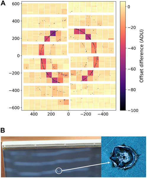
FIGURE 12. (A) Radiation damage resulting from an excessively intense X-ray diffraction signal (signal above the detector saturation point) from a powder sample. Entire ASICs are affected, although the signal was focused only on the sharp ring visible in the picture. (B) Radiation damage caused by exposure to a high-intensity X-ray diffraction signal generated by a 20 keV beam on a diamond anvil cell.
4.5 Data volume
The AGIPD detectors at the European XFEL are among the most frequently used MHz detectors at the facility, contributing to more than 80% of the total raw data. This significant contribution is mainly attributed to the detectors’ MHz operation. Furthermore, the unique design of the AGIPD detectors, which incorporates analog gain information alongside the images, significantly increases the data volume. The gain encoding process, due to the reasons discussed in Section 3.3, is performed “offline” and not in the detector back-end electronics, involving FPGAs as originally planned.
The data recorded at the European XFEL continues to accumulate rapidly and is approaching the 100 petabyte mark, necessitating a robust data volume management and data reduction strategy. To address this challenge of data volume, the European XFEL has devised a comprehensive strategy [49]. This approach encompasses early data reduction planning within the Data Management Plan (DMP), the development of operation-specific and technique-specific data reduction methods, enabling real-time data reduction for new experiments, and facilitating retroactive data reduction for previously collected data in collaboration with users. It also underscores the importance of integrating data reduction capabilities closer to the detector head, including within the ASIC or detector back-end electronics, as a critical consideration for the design of future detectors.
5 Insights for next-generation detector development
Over years of operation, the AGIPD detectors have consistently demonstrated their ability to deliver high-quality scientific results, as discussed in Section 4.1. Concurrently, data collection and dedicated studies have brought to light challenges that impact detector performance and scientific measurements. These challenges, although demanding, have provided invaluable experience and insights. This knowledge will be instrumental in shaping future detector projects for the European XFEL, offering valuable lessons that extend beyond the facility itself.
5.1 Effective scheduling and collaboration
Accurate project scheduling in research and development can present significant challenges. In 2006, the European XFEL issued a call for proposals to develop a MHz 2D Imaging Detector, leading to three projects, one of which was AGIPD. The first AGIPD1M detector became operational in mid-2017. Comparable timelines were observed in other detector projects at the European XFEL, including LPD and DSSC. Therefore, prudent planning that involves contingencies and realistic expectations regarding the development timeline, potentially spanning around a decade, is advisable.
Early collaboration with instrument experts, detector end users, and system integration, control, and data acquisition teams is of paramount importance. This collaboration helps ensure harmonious alignment of scientific and technical requirements, covering aspects such as infrastructure and control systems, between the detector developers and the ultimate users.
5.2 Detector system integration and operation
During the integration of detectors, such as AGIPD1M, a complex process unfolds, with a strong emphasis on convenience and ease of operation. Considerations in designing the detector’s mechanical interfaces to the rest of the instrument, as well as detector internal/external components, should ensure accessibility to cables, connectors, and internal detector components, simplifying replacement and repair processes. In particular, components exposed to X-rays are susceptible to damage, underscoring the importance of spare parts availability and straightforward repair procedures.
To streamline integration, efforts to simplify the power supply system and optimize the power consumption of the detector can significantly reduce complexity. This includes minimizing the number and thickness of power cables, enhancing the flexibility of the system, and mitigating the risk of potential damage during detector movement. Although this aspect has been partially addressed in the design of new-generation AGIPD detectors, more work can be done.
Efforts to reduce power consumption can also positively affect detector cooling requirements, as discussed in Section 2.3. Achieving optimal temperatures for detector components within a vacuum environment remains a challenge. Future detector developments should consider careful optimization of cooling system design, electronics design, and power dissipation to ensure desirable outcomes.
Furthermore, optimizing the design of electronic boards is essential to maximize the active area of the detector that relates to the entire system, particularly in instruments with limited space.
It should be noted that the adoption of a modular system with minimal critical components for the entire detector assembly can prove beneficial. If such functionality is necessary, the components should ideally be located outside the detector assembly vessel. This approach enables efficient component replacement in a short time frame, typically minutes to hours, without extensive effort. In the case of AGIPD1M detectors, composed of two electronically independent halves, the control of each half is managed through the master FPGA. However, this concept presents some disadvantages, such as the loss of half of the detector’s functionality in the case of a board failure. The design of the next-generation of AGIPD detectors, which addresses these concerns through redesigned back electronics, is promising.
Another vital but often overlooked aspect is the detector safety system. The interlock system developed for the AGIPD1M detectors effectively protects them against unexpected failures (e.g., vacuum or cooling failure) and potential human errors. Over years of operation at the European XFEL, this system has prevented more than ten accidents, including damage from water condensation on electronics due to vacuum failure or component overheating due to cooling issues. However, as mentioned in Section 2.4, the AGIPD1M interlock system relies on external PLC-based interlocks that monitor temperature and pressure sensors within the detector vessel and act accordingly. This increases the infrastructure of the detector, requiring a more self-protecting system. Therefore, ensuring detector safety must begin at the design level, implementing a simple, reliable and ideally self-protecting system to minimize the risk of detector damage.
However, there are cases where protection is not always feasible, as exemplified by radiation damage, discussed in Section 4.4. Therefore, the mitigation of radiation damage in the ASIC is a critical aspect of future detector development for high-intensity X-ray sources.
Finally, the significance of data quality cannot be overstated in determining the performance of the detector. Achieving high-quality data is highly dependent on the precise calibration and characterization of the detectors. This process is not a one-time activity, but must be conducted regularly, even during user experiments, to address incidents that may impact data quality. The utilization of internal calibration sources, such as the Pulsed Capacitor (PC) and Current Source (CS), facilitates routine dynamic range scans. Nevertheless, it is worth noting that both sources possess limitations, as discussed in Section 3.4. Therefore, prioritizing the development of a reliable, “in-situ” calibration mechanism, particularly at the ASIC level, becomes imperative for the progression of future detector generations.
5.3 Testing the system under real conditions
Comprehensive testing of a detector system can only be achieved under actual operational conditions. This necessitates evaluating the detector at its full size, within the final installation infrastructure, and, in our case, in the presence of the European XFEL beam. The absence of the beam during the detector’s development phase left certain features unidentified and unaddressed until the detector was fully assembled and installed. Consequently, it is advisable for any new detector project to test its prototype under conditions that closely resemble the final operational environment, with a focus on considering scalability from the project’s inception.
When delving into particulars of the chip design, several key observations were brought to light that could be beneficial for forthcoming development projects.
1. Data quality is influenced by the utilization of an analog memory matrix for storing image data on pixel before it can be transferred from the detector head. Challenges are posed by variations in offset and gain, which depend on the index (position) of the memory cell in the pixel and the leakage into neighboring memory cells that leads to the issue of gain encoding as described in Section 3.3. To enhance data quality, the requirement of generating calibration constants for each memory cell in the pixel should be reconsidered. In the next-generation of detectors, it is proposed that exploration of options such as digital storage cells or alternatives to existing storage cells be undertaken, with the potential to enable real-time data transfer from Front-End Modules (FEMs).
2. The achievement of a high dynamic range through an adaptive gain mechanism is accompanied by challenges related to linearity and data quality, particularly in the transition region between gain settings. Comparable issues have been noted in other detectors that employ adaptive gain mechanisms, such as JUNGFRAU [50]. To address these concerns, the exploration of alternative implementations and solutions aimed at realizing a high dynamic range or a more robust design of the adaptive gain switching mechanism, preventing the aforementioned “late gain switching” and avoiding the transition region between different gain settings, is deemed to be imperative. This is of paramount importance, as the dynamic range remains a critical parameter to be realized in the next-generation of detectors.
6 Conclusion and outlook
The AGIPD detector systems deployed at the European XFEL instruments have demonstrated their reliability and made a significant contribution to the generation of valuable scientific data, as evidenced by numerous scientific publications. This underscores their ability to support experiments with specific demands, provided that their characteristics and limitations are well understood.
A commitment to continuous improvement and development in the operation of the AGIPD detectors has resulted in substantial benefits, leveraging the expertise of detector specialists and beamline instrument scientists with a range of backgrounds. Through hardware optimization, enhanced detector characterization, and advanced data processing techniques, we have effectively accommodated diverse experiment requests and acquired reliable scientific data. Regular maintenance, updates, and innovative data processing have collectively increased the quality of AGIPD-generated data.
However, it is essential to acknowledge that AGIPD optimization remains an ongoing process. Collaborative efforts that draw upon the expertise of individuals with diverse backgrounds remain essential components in optimizing detector performance and addressing observed issues.
Looking ahead, the second generation of AGIPD detectors, slated for installation in 2024 at the HED instrument (one-megapixel system) and the SPB/SFX instrument (four-megapixel system), represents a significant step forward. A prototype of the new detectors is already in use at HED, with the first results from user experiments already published. Although certain challenges discussed in this publication have been addressed in the second-generation AGIPD, not all have been resolved. As emphasized in this paper, the redesign of key detector components, such as the ASIC, is essential to effectively address these challenges.
The operational insights gained from AGIPD detectors will play a valuable role in shaping the future of the detector development program at the European XFEL. The integration of the initial detector generation into the European XFEL instruments was a formidable undertaking, revealing infrastructure challenges for integration and operation. To address these challenges, we emphasize the need for more compact and efficient power and cooling designs with standardized interfaces.
Our experiences underscore the importance of ease of operation and reliability, accessible detector components for maintenance and replacement, and the critical role of hardware interlocks, including the consideration of self-protecting detectors. Furthermore, the management of the substantial volume of generated data requires early design-level data reduction strategies.
Data quality remains the paramount measure of detector performance, highlighting the necessity of evaluating methods to achieve high dynamic range, exploring alternative solutions for storing data at pixel level instead of relying on analog memory cells, and designing calibration-friendly systems with reliable in-situ calibration sources.
Although the scientific requirements for the initial years of instrument operation are met by current detectors to the largest extent, plans for the next-generation of detectors are well underway. The demand for smaller pixel sizes, extended dynamic range, and the ability to operate at MHz rates while recording even more pulses per second are the primary driving factors behind the search for innovative technological solutions. Transitioning from 130 to 65 or 28 nm CMOS technology and exploring three-dimensional integrated electronic circuits may offer promising avenues for addressing these challenges. Additionally, the development of edgeless sensors holds potential for minimizing inactive detector areas. Furthermore, the imperative of maintaining high quantum efficiency, even at energies exceeding 20 keV, motivates the exploration of materials with atomic numbers higher than those of silicon.
With the prospect of developing novel detectors for the post-2030 European XFEL operation, the insights and experiences gained from the AGIPD detector operation, in conjunction with the ever-evolving scientific requirements, constitute indispensable foundations for shaping the future of detector technology for the European XFEL.
Author contributions
JS-D: Conceptualization, Data curation, Formal Analysis, Investigation, Methodology, Project administration, Supervision, Validation, Writing–original draft. VR: Investigation, Methodology, Validation, Writing–review and editing. AK: Investigation, Methodology, Validation, Writing–review and editing. TL: Investigation, Methodology, Validation, Writing–review and editing. UT: Conceptualization, Investigation, Methodology, Writing–review and editing, Validation. KA: Software, Visualization, Writing–review and editing. OM: Validation, Writing–review and editing. JM: Methodology, Validation, Investigation, Writing–review and editing. AP: Software, Writing–review and editing. NR: Investigation, Validation, Writing–review and editing. RS: Validation, Writing–review and editing. MS: Investigation, Validation, Writing–review and editing. GA: Conceptualization, Validation, Writing–review and editing. UB: Investigation, Validation, Writing–review and editing. LL: Conceptualization, Validation, Writing–review and editing. AM: Software, Writing–review and editing. TP: Validation, Writing–review and editing. PS: Software, Writing–review and editing. SS: Investigation, Validation, Writing–review and editing. RB: Resources, Writing–review and editing. AM: Resources, Writing–review and editing. LG: Resources, Writing–review and editing. SH: Methodology, Resources, Software, Writing–review and editing. PG: Resources, Writing–review and editing. KW: Resources, Writing–review and editing. HG: Project administration, Resources, Writing–review and editing. MT: Resources, Writing–review and editing.
Funding
The author(s) declare that no financial support was received for the research, authorship, and/or publication of this article.
Acknowledgments
The authors thank the AGIPD consortium for developing the AGIPD detectors for the European XFEL. We acknowledge European XFEL in Schenefeld, Germany, for provision of X-ray free-electron laser beamtime at Scientific Instrument SPB/SFX (Single Particles, Clusters, and Biomolecules and Serial Femtosecond Crystallography) and Scientific Instrument MID (Materials Imaging and Dynamics) and would like to thank the staff for their assistance. We also acknowledge support from DESY (Hamburg, Germany), a member of the Helmholtz Association HGF. Furthermore, the authors express their gratitude to the Data Department groups, including Controls, IT and Data Management, and Electronics and Electrical Engineering, for their significant contributions to detector integration and Data Analysis for providing the software tools for detector data analysis.
Conflict of interest
The authors declare that the research was conducted in the absence of any commercial or financial relationships that could be construed as a potential conflict of interest.
Publisher’s note
All claims expressed in this article are solely those of the authors and do not necessarily represent those of their affiliated organizations, or those of the publisher, the editors and the reviewers. Any product that may be evaluated in this article, or claim that may be made by its manufacturer, is not guaranteed or endorsed by the publisher.
References
1. Decking W, Abeghyan S, Abramian P, Abramsky A, Aguirre A, Albrecht C, et al. A mhz-repetition-rate hard x-ray free-electron laser driven by a superconducting linear accelerator. Nat Photon (2020) 14:391–7. doi:10.1038/s41566-020-0607-z
2. Tschentscher T. Investigating ultrafast structural dynamics using high repetition rate x-ray fel radiation at european xfel. The Eur Phys J Plus (2023) 138:274. doi:10.1140/epjp/s13360-023-03809-5
3. Mancuso AP, Aquila A, Batchelor L, Bean RJ, Bielecki J, Borchers G, et al. The single particles, clusters and biomolecules and serial femtosecond crystallography instrument of the european xfel: initial installation. J Synchrotron Radiat (2019) 26:660–76. doi:10.1107/S1600577519003308
4. Galler A, Gawelda W, Biednov M, Bomer C, Britz A, Brockhauser S, et al. Scientific instrument Femtosecond X-ray Experiments (FXE): instrumentation and baseline experimental capabilities. J Synchrotron Radiat (2019) 26:1432–47. doi:10.1107/S1600577519006647
5. Madsen A, Hallmann J, Ansaldi G, Roth T, Lu W, Kim C, et al. Materials imaging and dynamics (MID) instrument at the European X-ray free-electron laser facility. J Synchrotron Radiat (2021) 28:637–49. doi:10.1107/S1600577521001302
6. Zastrau U, Appel K, Baehtz C, Baehr O, Batchelor L, Berghäuser A, et al. The high energy density scientific instrument at the European XFEL. J Synchrotron Radiat (2021) 28:1393–416. doi:10.1107/S1600577521007335
7. Tschentscher T, Bressler C, Grünert J, Madsen A, Mancuso AP, Meyer M, et al. Photon beam transport and scientific instruments at the European XFEL. Appl Sci (2017) 7:592. doi:10.3390/app7060592
8. Mazza T, Baumann TM, Boll R, De Fanis A, Grychtol P, Ilchen M, et al. The beam transport system for the Small Quantum Systems instrument at the European XFEL: optical layout and first commissioning results. J Synchrotron Radiat (2023) 30:457–67. doi:10.1107/S1600577522012085
9. Graafsma H. Requirements for and development of 2 dimensional x-ray detectors for the European X-ray free electron laser in Hamburg. J Instrumentation (2009) 4:P12011. doi:10.1088/1748-0221/4/12/p12011
10. Veale MC, Adkin P, Booker P, Coughlan J, French MJ, Hart M, et al. Characterisation of the high dynamic range large pixel detector (lpd) and its use at x-ray free electron laser sources. J Instrumentation (2017) 12:P12003. doi:10.1088/1748-0221/12/12/P12003
11. Allahgholi A, Becker J, Delfs A, Dinapoli R, Goettlicher P, Greiffenberg D, et al. The adaptive gain integrating pixel detector at the European XFEL. J Synchrotron Radiat (2019) 26:74–82. doi:10.1107/S1600577518016077
12. Porro M, Andricek L, Aschauer S, Castoldi A, Donato M, Engelke J, et al. The MiniSDD-based 1-mpixel camera of the DSSC project for the European XFEL. IEEE Trans Nucl Sci (2021) 68:1334–50. doi:10.1109/TNS.2021.3076602
13. Shi X, Dinapoli R, Henrich B, Mozzanica A, Schmitt B, Mazzocco R, et al. Challenges in chip design for the agipd detector. Nucl Instr Methods Phys Res Section A: Acc Spectrometers, Detectors Associated Equipment (2010) 624:387–91. doi:10.1016/j.nima.2010.05.038
14. Schwandt J, Fretwurst E, Klanner R, Kopsalis I, Zhang J. Design and first tests of a radiation-hard pixel sensor for the european x-ray free-electron laser. In: 2013 14th European Conference on Radiation and Its Effects on Components and Systems (RADECS); 23-27 September 2013; Oxford, UK (2013). p. 1–8. doi:10.1109/RADECS.2013.6937446
15. Mezza D, Allahgholi A, Arino-Estrada G, Bianco L, Delfs A, Dinapoli R, et al. Characterization of agipd1.0: the full scale chip. Nucl Instr Methods Phys Res Section A: Acc Spectrometers, Detectors Associated Equipment (2016) 838:39–46. doi:10.1016/j.nima.2016.09.007
16. Mezza D, Allahgholi A, Becker J, Delfs A, Dinapoli R, Goettlicher P, et al. Characterization of the agipd1.1 readout chip and improvements with respect to agipd1.0. Nucl Instr Methods Phys Res Section A: Acc Spectrometers, Detectors Associated Equipment (2019) 945:162606. doi:10.1016/j.nima.2019.162606
17. Zhang J, Fretwurst E, Graafsma H, Klanner R, Kopsalis I, Schwandt J. Study of x-ray radiation damage in the agipd sensor for the european xfel. J Instrumentation (2014) 9:C05022. doi:10.1088/1748-0221/9/05/C05022
18. Husband RJ, Strohm C, Appel K, Ball OB, Briggs R, Buchen J, et al. A MHz X-ray diffraction set-up for dynamic compression experiments in the diamond anvil cell. J Synchrotron Radiat (2023) 30:671–85. doi:10.1107/S1600577523003910
19. Allahgholi A, Becker J, Delfs A, Dinapoli R, Göttlicher P, Graafsma H, et al. Megapixels @ megahertz – the agipd high-speed cameras for the european xfel. Nucl Instr Methods Phys Res Section A: Acc Spectrometers, Detectors Associated Equipment (2019) 942:162324. doi:10.1016/j.nima.2019.06.065
20. Ball OB, Prescher C, Appel K, Baehtz C, Baron MA, Briggs R, et al. Dynamic optical spectroscopy and pyrometry of static targets under optical and x-ray laser heating at the european xfel. J Appl Phys (2023) 134:055901. doi:10.1063/5.0142196
21. Siska E, Smith GA, Villa-Cortes S, Conway LJ, Husband RJ, Cleave JV, et al. Ultra-fast yttrium hydride chemistry at high pressures via non-equilibrium states induced by x-ray free electron laser (2023).
22. Wiener-D. MPOD modules (2023). Available from: https://www.wiener-d.com/modules/mpod-modules/ (Accessed on September 28, 2023).
23. Flaschel N, Ariza D, Díez S, Gerboles M, Gregor IM, Jorda X, et al. Thermal and hydrodynamic studies for micro-channel cooling for large area silicon sensors in high energy physics experiments. Nucl Instr Methods Phys Res Section A: Acc Spectrometers, Detectors Associated Equipment (2017) 863:26–34. doi:10.1016/j.nima.2017.05.003
24. Coppola N, Tolkiehn J, Youngman C. Control using beckhoff distributed rail systems at the european xfel. In: Proceedings of ICALEPCS 2013; October 6-11, 2013; San Francisco, CA, USA (2013). p. TUPPC046.
25. Hauf S, Heisen B, Aplin S, Beg M, Bergemann M, Bondar V, et al. The Karabo distributed control system. J Synchrotron Radiat (2019) 26:1448–61. doi:10.1107/S1600577519006696
26. Rehlich K, Aghababyan A, Kay H, Petrosyan G, Petrosyan L, Petrosyan V, et al. The new timing system for the european xfel (2013).
27. Koranne S. Hierarchical data format 5: HDF5. Boston, MA: Springer US (2011). p. 191–200. doi:10.1007/978-1-4419-7719-9_10
28. Schmuck F, Haskin R. Gpfs: a shared-disk file system for large computing clusters. In: Proceedings of the FAST’02 Conference on File and Storage Technologies (Monterey, California, US: USENIX); January 28-30, 2002; Monterey, California, USA (2002). p. 231–44. Retrieved 2008-01-18.
31. European XFEL. Calibration catalogue (2023). Available from: https://in.xfel.eu/calibration.
32. Schmidt P, Ahmed K, Danilevski C, Hammer D, Rosca R, Kluyver T, et al. Turning european xfel raw data into user data. Front Phys (2023) 11. doi:10.3389/fphy.2023.1321524
33. Mezza D, Becker J, Carraresi L, Castoldi A, Dinapoli R, Goettlicher P, et al. Calibration methods for charge integrating detectors. Nucl Instr Methods Phys Res Section A: Acc Spectrometers, Detectors Associated Equipment (2022) 1024:166078. doi:10.1016/j.nima.2021.166078
34. Chapman HN, Fromme P, Barty A, White TA, Kirian RA, Aquila A, et al. Femtosecond x-ray protein nanocrystallography. Nature (2011) 470:73–7. doi:10.1038/nature09750
35. Kirkwood HJ, de Wijn R, Mills G, Letrun R, Kloos M, Vakili M, et al. A multi-million image serial femtosecond crystallography dataset collected at the european xfel. Scientific Data (2022) 9:161. doi:10.1038/s41597-022-01266-w
36. Pandey S, Calvey G, Katz AM, Malla TN, Koua FHM, Martin-Garcia JM, et al. Observation of substrate diffusion and ligand binding in enzyme crystals using high-repetition-rate mix-and-inject serial crystallography. IUCrJ (2021) 8:878–95. doi:10.1107/S2052252521008125
37. Wiedorn MO, Oberthür D, Bean R, Schubert R, Werner N, Abbey B, et al. Megahertz serial crystallography. Nat Commun (2018) 9:4025. doi:10.1038/s41467-018-06156-7
38. Ayyer K, Xavier PL, Bielecki J, Shen Z, Daurer BJ, Samanta AK, et al. 3d diffractive imaging of nanoparticle ensembles using an x-ray laser. Optica (2021) 8:15–23. doi:10.1364/OPTICA.410851
39. Sobolev E, Zolotarev S, Giewekemeyer K, Bielecki J, Okamoto K, Reddy HKN, et al. Megahertz single-particle imaging at the european xfel. Commun Phys (2020) 3:97. doi:10.1038/s42005-020-0362-y
40. Lehmkühler F, Dallari F, Jain A, Sikorski M, Möller J, Frenzel L, et al. Emergence of anomalous dynamics in soft matter probed at the european xfel. Proc Natl Acad Sci (2020) 117:24110–6. doi:10.1073/pnas.2003337117
41. Grünbein ML, Bielecki J, Gorel A, Stricker M, Bean R, Cammarata M, et al. Megahertz data collection from protein microcrystals at an x-ray free-electron laser. Nat Commun (2018) 9:3487. doi:10.1038/s41467-018-05953-4
42. Grünbein ML, Bielecki J, Gorel A, Stricker M, Bean R, Cammarata M, et al. Mhz data collection of a microcrystalline mixture of different jack bean proteins. Scientific Data (2019) 6:18. doi:10.1038/s41597-019-0010-0
43. Dallari F, Reiser M, Lokteva I, Jain A, Möller J, Scholz M, et al. Analysis strategies for mhz xpcs at the european xfel. Appl Sci (2021) 11:8037. doi:10.3390/app11178037
44. Dallari F, Jain A, Sikorski M, Möller J, Bean R, Boesenberg U, et al. Microsecond hydrodynamic interactions in dense colloidal dispersions probed at the European XFEL. IUCrJ (2021) 8:775–83. doi:10.1107/S2052252521006333
45. Dallari F, Lokteva I, Möller J, Jain A, Roseker W, Westermeier F, et al. Coherence properties from speckle contrast analysis at the european xfel. J Phys Conf Ser (2022) 2380:012085. doi:10.1088/1742-6596/2380/1/012085
46. Reiser M, Girelli A, Ragulskaya A, Das S, Berkowicz S, Bin M, et al. Resolving molecular diffusion and aggregation of antibody proteins with megahertz x-ray free-electron laser pulses. Nat Commun (2022) 13:5528. doi:10.1038/s41467-022-33154-7
47. Dallari F, Lokteva I, Möller J, Roseker W, Goy C, Westermeier F, et al. Real-time swelling-deswelling kinetics of nanogels driven by xfel pulses. in preparation (2023).
48. Trost F, Ayyer K, Prasciolu M, Fleckenstein H, Barthelmess M, Yefanov O, et al. Imaging via correlation of x-ray fluorescence photons. Phys Rev Lett (2023) 130:173201. doi:10.1103/PhysRevLett.130.173201
49. Sobolev E, Schmidt P, Malka J, Hammer D, Boukhelef D, Dall’Antonia F, et al. Reducing big data at the european xfel. Front Phys (2023). Paper in preparation.
Keywords: MHz X-ray detectors, 2D detectors, FEL instrumentation, calibration, adaptive gain
Citation: Sztuk-Dambietz J, Rovensky V, Klujev A, Laurus T, Trunk U, Ahmed K, Meyer O, Möller J, Parenti A, Raab N, Shayduk R, Sikorski M, Ansaldi G, Bösenberg U, Luis LM, Muenich A, Preston TR, Schmidt P, Stern S, Bean R, Madsen A, Gelisio L, Hauf S, Gessler P, Wrona K, Graafsma H and Turcato M (2024) Operational experience with Adaptive Gain Integrating Pixel Detectors at European XFEL. Front. Phys. 11:1329378. doi: 10.3389/fphy.2023.1329378
Received: 28 October 2023; Accepted: 18 December 2023;
Published: 26 February 2024.
Edited by:
Ki Hyun Nam, Kookmin University, Republic of KoreaReviewed by:
Carlo Fiorini, Polytechnic University of Milan, ItalyGiovanni Di Domenico, University of Ferrara, Italy
Copyright © 2024 Sztuk-Dambietz, Rovensky, Klujev, Laurus, Trunk, Ahmed, Meyer, Möller, Parenti, Raab, Shayduk, Sikorski, Ansaldi, Bösenberg, Luis, Muenich, Preston, Schmidt, Stern, Bean, Madsen, Gelisio, Hauf, Gessler, Wrona, Graafsma and Turcato. This is an open-access article distributed under the terms of the Creative Commons Attribution License (CC BY). The use, distribution or reproduction in other forums is permitted, provided the original author(s) and the copyright owner(s) are credited and that the original publication in this journal is cited, in accordance with accepted academic practice. No use, distribution or reproduction is permitted which does not comply with these terms.
*Correspondence: Jolanta Sztuk-Dambietz, jolanta.sztuk@xfel.eu
‡Previously known as Ivana Klačková
§Previously known as Alexander Klyuev
†Present address: Stephan Stern, X-Spectrum GmbH, Hamburg, Germany