A refractive index sensor based on metal-insulator-metal coupling ring resonator with a stub
 Yuhao Cao1,2,3
  Shubin Yan2,3* Feng Liu1,2,3 Jin Wang1,2,3 Shuwen Chang1,2,3 Guang Liu2,3 Wei Zhang2,3 Taiquan Wu2,3 Yifeng Ren1
- 1School of Electrical and Control Engineering, North University of China, Taiyuan, China
- 2School of Electrical Engineering, Zhejiang University of Water Resources and Electric Power, Hangzhou, China
- 3Joint Laboratory of Intelligent Equipment and System for Water Conservancy and Hydropower Safety Monitoring of Zhejiang Province and Belarus, Hangzhou, China
In this work, a refractive index sensor structure is proposed, which consists of the met-al-insulator-metal (MIM) waveguide coupling with ring resonator with a rectangular cavity. Its sensing characteristics are analyzed by the finite element analysis method. SPPs is an electromagnetic wave mode excited by the oscillatory coupling of free electron-photon interactions on the surface region of a metal, whose field strength is maximum at the metal-dielectric partition interface and then decays exponentially to both sides The results show that the sensing characteristics of the ring resonator can be changed by introducing a stub, which can achieve the purpose of enhancing the coupling efficiency of SPPs. The structure has two Fano peaks, and each peak can be individually regulated by changing the size of the sensing structure. Sensitivity is the key performance indicator of the system, which is the shift in resonance wavelength caused by a change in refractive index when the ambient medium is changed. The best sensitivity of this structure can reach 2,300 nm/RIU with a figure of merit (FOM) value of 60 RIU−1. The proposed structure has great potential in nano-sensors.
1 Introduction
Surface plasmon polaritons (SPPs) are generated by electrons under the influence of an external electromagnetic field [1, 2]. Its essence is an electromagnetic wave mode excited by the interaction of free electrons and photons on the metal surface area [3, 4]. The field strength is the largest at the interface of the metal medium. The exponential form decays to both sides. SPPs can break through the optical diffraction limit of traditional optics, thereby realizing the adjustment and transmission of light at sub-wavelengths [5, 6].
Resonant phenomena are the tendencies of a physical system to absorb more energy from the environment when it is near the natural frequency of oscillation (called the resonant frequency) and near the natural wavelength. Unlike the symmetrical Lorentz resonance, Fano resonance is an asymmetric line-shaped scattering resonance phenomenon, which usually occurs during the coupling of the SPPs [7]. Hence, it has a high spatial electromagnetic field confinement ability, and can better identify small frequency shifts [8]. Various SPP based light devices were born, such as refractive index sensors [9–13], slow light devices [14, 15], optical switches [16, 17], biosensors [18–24], etc. Because the resonator structure is also an important factor in generating Fano resonance, rectangular resonators, annular resonators, semi-ring resonators, tie resonators, etc. All exhibit different sensing characteristics due to different structures, such as in [12], who designed a plasmon system coupled with a MIM waveguide and a ring cavity, and its sensitivity can reach 1,600 nm/RIU. It achieves coordinated multiple Fano resonances and similar electromagnetic transparency effects [25]. Chau-Yuan Fong Chou et al. designed a sensor structure of a MIM waveguide coupled with an elliptical resonator with a stub, and by embedding an air path in the MIM waveguide to increase its coupling efficiency, the performance of the sensor was greatly improved [26]. [18] proposed a sensor structure of a MIM waveguide coupled with a rectangular ring resonator with defects. By changing the position, number and other parameters of the defects, it was proved that under certain conditions, the symmetrical resonator structure, the anti-symmetric mode cannot be stimulated. The sensitivity of the improved structure can reach 1,850 nm/RIU [27].
A necessary condition for the creation of Fano resonance is the simultaneous generation of high-level multi-order sub-radiative and super-radiative modes. The subsequent overlapping coupling behavior of these modes is guaranteed. In some structures, there will be a situation where the structure is extremely symmetrical, and the dipole resonance mode and the higher-order resonance mode will be converted in-to orthogonal coupling, and the coupling cannot be overlapped at this time. In this case, it is necessary to modify the degree of symmetry of the structure, that is, to adjust the structural model. Or directly use asymmetric structures to excite bright and dark states to generate Fano resonance waveforms. This is a common approach in designing optical sensor structures, where the microstructure can be altered so that enough light can be confined to the gas sample to increase the interaction between the light and the sample. For example, the photonic crystal fiber based high sensitivity, low confinement loss gas sensor designed by [28] The insertion of circular dot matrix air holes in the core region and hexagonal dot matrix air holes in the cladding region allows more swift waves to pass through the cladding holes and interact with the detected gas, thus increasing the relative sensitivity of the gas sensor. In most of the previous articles, the coupling efficiency was increased by changing the structure and the MIM waveguide. In this paper, we try to embed a simple rectangular cavity (stub-2) into the ring structure to break the symmetry structure, and investigate whether Fano can exhibit different characteristics. In this work, we propose a MIM waveguide structure. This structure includes the MIM bus waveguide with a rectangular cavity (stub-1) and a ring resonator with stub-2. Stub-2 is used to break the symmetric structure to obtain different sensing characteristics. In-depth study of the influence of different parameters on Fano curve, sensitivity S, figure of merit (FOM) and other parameters.
2 Geometry structure and analysis methods
The structure model is built with COMSOL Multiphysics 5.4. We used the FEM to analyze the transmission performance exhibited by the SPPs. Most researchers of MIM plasmonic sensors make the height infinite because the height affects the loss of the waveguide. This phenomenon is due to the inverse relationship between the height and the real and imaginary parts of the effective refractive index. As the height increases, the real and imaginary parts decrease and remain stable for infinite height values. And only under the irradiation of the TM wave mode, the metal-dielectric interface layer will produce SPPs. For the TM mode, the electromagnetic wave propagates forward along the xoy plane, so we can build a two-dimensional model to study SPPs [29]. Above and below of the structure, we set up boundary conditions for a perfectly matched layer that absorbs the waves escaping from the structure (The size of the model is 1,320 nm
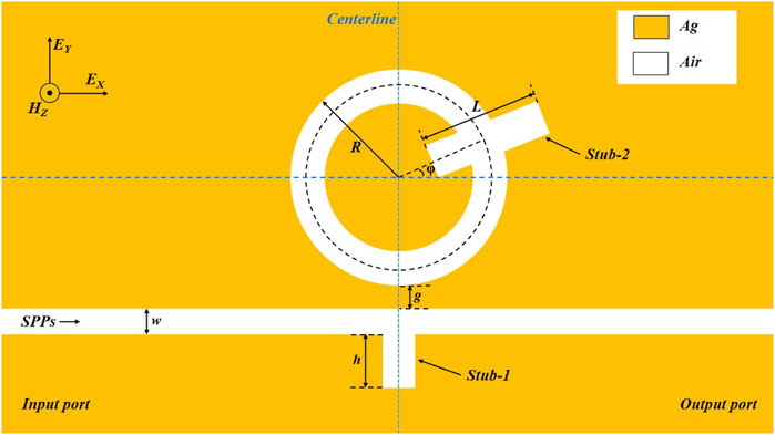
FIGURE 1. Two-dimension structure.
In Eq. (1), k represents the wave loss in the waveguide.
The mental (orange area) and insulator material (while area) represented silver and air. The silver was chosen as a filler metal because it had a low imaginary part of the relative permittivity in the near-infrared range, resulting in low power consumption. The relative dielectric constant of silver is defined by the Debye-Drude dispersion model [31]:
In Eq. (2), the relative permittivity of infinite frequencies (
The performance of the sensor can be expressed by sensitivity and FOM, which defined are as follow [32, 33]:
In Eq. (3),
Resonant wavelength expressions:
where D represents the effective side length of the resonant cavity,
3 Simulation results and analysis
Firstly, we studied the difference between a single stub structure (red line), a single ring structure (blue line), and the entire structure (green line) to understand the cause of Fano resonance, as shown in Figure 2A–C. Its specific parameters are set as following: R = 220 nm, h = 50 nm, L = 200 nm, g = 10 nm,
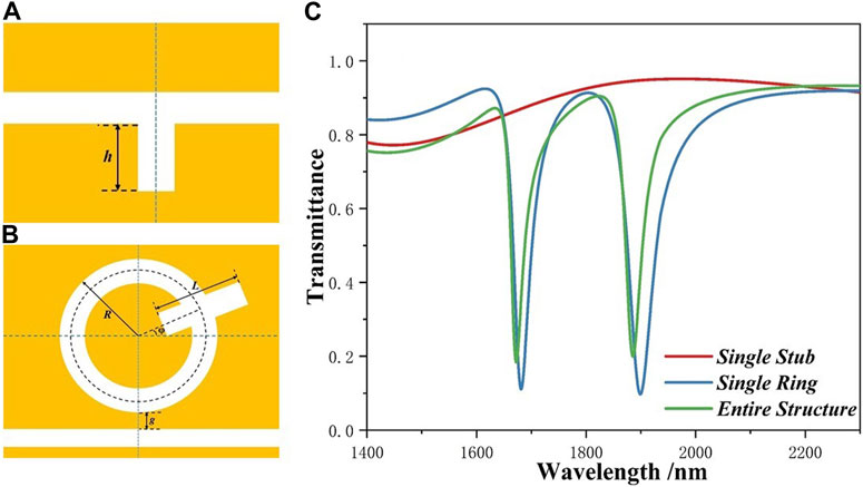
FIGURE 2. (A) Single stub structure; (B) Single ring structure; (C) Transmittance spectrums.
In order to study how the
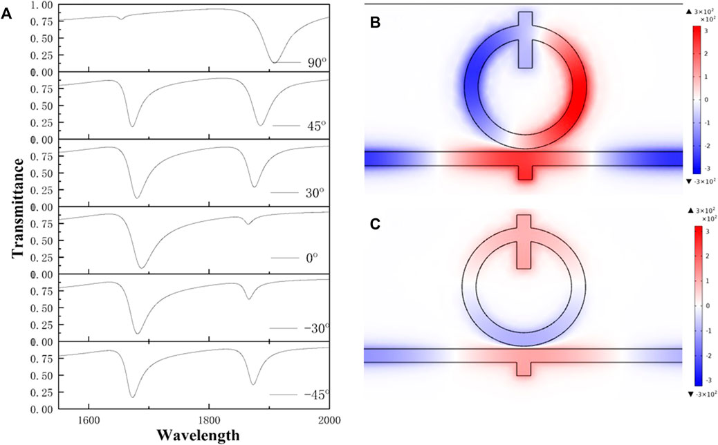
FIGURE 3. (A) Transmittance spectrums at different angles; (B) Magnetic field intensity in the FR1 (
Next, the mode order of the structure is calculated from the magnetic field normalisation diagram. Taking FR1 as an example, when the incident wavelength is 1,601 nm, the effective edge length of the SPPs:
Subsequently, we studied how the R parameter value affects the system performance. The different parameter R settings are as follows: 180 nm, 190 nm, 200 nm, 210 nm, 220 nm. Its spectrums chart and sensitivity image are depicted in Figures 4A, B. With the increase of the outer radius R, the curve has a red shift phenomenon, its dip position has moved from 1,541 nm to 1,885 nm and the sensitivity has enhanced from 1,540 nm/RIU to 2,300 nm/RIU. This result also proves that the RRS acts as a narrow discrete state, and if its outer radius is changed, it will have an effect on the performance of the system. At the same time, we can also use the resonant wavelength formula to explain this phenomenon. When R (that is, the effective wavelength L) increases, the wave-length will increase, so that the position of the dip shifts to the right. When R = 220 nm, the sensitivity reaches 2,300 nm/RIU and has a FOM of 64.24 RIU−1, which is better than the data in Table 1. But this does not mean that the larger R the better, we need to consider the transmittance, FOM, and the required wavelength of the laser.
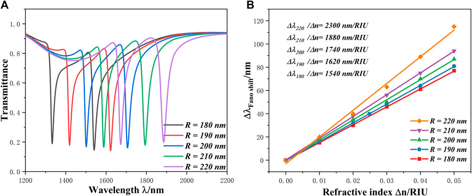
FIGURE 4. (A) Change in transmittance obtained via COMSOL simulations, as radius of the waveguide R is varied from 180 nm to 220 nm with a interval of 10 nm; (B) Sensitivity change images of R from 180 nm to 220 nm with a interval of 10 nm.
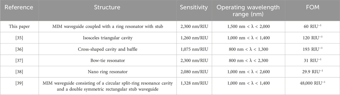
TABLE 1. Comparison of performance of different structures.
Moreover, the influences of the L parameter on system performance were studied, and its parameters are set as follows: L = 150 nm, 175 nm, 200 nm, 225 nm, and 250 nm. From Figure 5A, the change of L will not affect FR1, but for FR2, the curve is red-shifted and the inclination position becomes larger. In order to explore the reasons for this phenomenon, we have drawn their normalized Hz field maps. Observed from Figures 5B, C, a node of FR1 is located on the stub, while the node of FR2 is not on the stub. The number of nodes is also used to reflect the intensity of the normalized Hz field. The more the number, the weaker the intensity. However, there is no normalized Hz field at the stub of FR1, so the influence of L change on it is weak, and whether the two ends of stub-2 are in-phase or out-of-phase will also show different system performance to a certain extent. Hence, we can achieve the separate modulation of FR2 by change L.
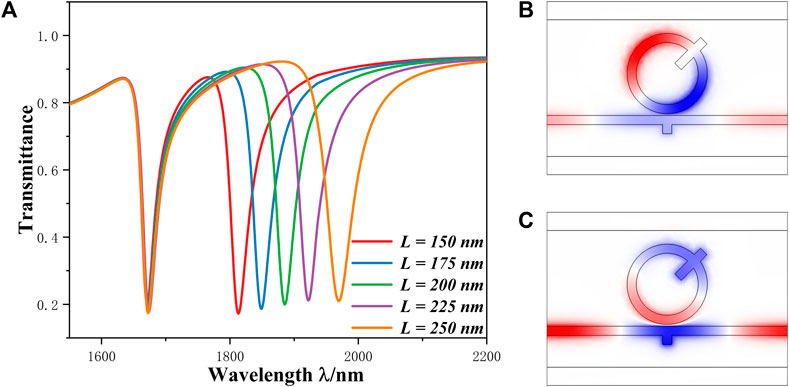
FIGURE 5. (A) Change in transmittance obtained via COMSOL simulations, as length of stub-2 (L) is varied from 150 nm to 220 nm with a interval of 25 nm; (B) Magnetic field intensity in the FR1 (
We changed the parameters of g from 25 nm to 5 nm at intervals of 5 nm to observe the characteristics of the system. From Figure 6A, we can observe that with the change of g, the transmittance minimum of the curve decreases sharply and the curve blue shifts, the resonance wavelength drifts significantly in the range from 5 nm to 15 nm, while there is little movement in the range from 15 nm to 25 nm. The reason for this phenomenon is that as the coupling distance increases, the binding between the waveguide and the resonant cavity becomes weaker and weaker, resulting in a significant weakening of the effective refractive index part of the coupling mode of the resonant cavity, which can be neglected when the coupling distance reaches a certain value. According to Eq. 5, when the coupling distance increases to 15 nm, the wavelength drift corresponding to the wave valley will be smaller as the structural parameters are fixed and the effective refractive index becomes smaller.
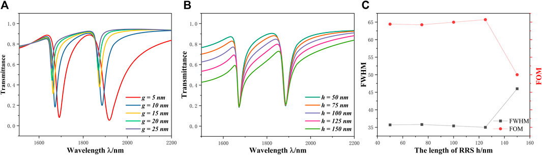
FIGURE 6. (A) Spectrum chart of diverse g from 5 nm to 25 nm with a interval of 5 nm; (B) Transmittance spectrums of different h from 50 nm to 150 nm with a interval of 25 nm; (C) FWHM image.
Subsequently, by changing the h parameter, its transmission spectrums and FWHM diagram are shown in Figures 6B, C. The change of the h parameter has almost no effect on the transmittance minimum and tilt position, but it will change the value of FWHM. When the value of S is constant, the FOM value will also change. It can be seen from Figure 6C when h = 125 nm, the FWHM is the narrowest, and the best performance at this time is: the sensitivity value of 2,300 nm/RIU and the FOM value of 65.71 RIU-1. Compared with the structural properties listed in Table 1, the structure can be excited at a smaller wavelength with higher sensitivity, but the FOM value will be slightly lower.
Finally, the principle of the plasma refractive index sensor is that the resonant tilt angle changes with the change of the refractive index, so when the structural parameters are fixed (i.e., R = 220 nm, h = 125 nm, L = 200 nm, g = 10 nm,
FIGURE 7. (A) Spectrum chart of the refractive index from 1.00 to 1.05; (B) Linear fitting of the sensitivity.
4 Application
The designed sensor structure is shown in Figure 8 and is mainly composed of a laser, a conical waveguide, an optical waveguide, a high-Q optical microcavity and an array of metal nanoparticles. The optical field is localed in a small cavity mode volume, high Q resonant cavity and transmitted in WGM mode, resulting in a strong abrupt field around the surface of the high Q microcavity, the conical waveguide region and the interaction with the specimen, and the excitation of metal nanoparticles on the surface of the microcavity generating Fano resonance peaks with extremely high sensitivity to the external environment.
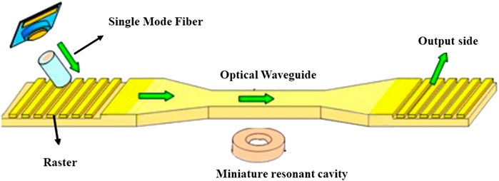
FIGURE 8. Schematic diagram of the sensing structure.
When the air medium in the resonant cavity is replaced with an ethanol solution it can be used as a temperature sensor, the essence of which is that when the temperature of the surrounding environment changes, the refractive index of the solution in the structure changes as well. Ethanol has a melting point of −114.3
T in the formula indicates the temperature to be measured,
The T in the equation represents the amount of change in the environment. Taking into account the limits of the detection range of the structure, we set the temperature to be measured to change from −40
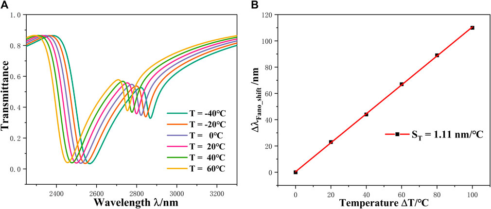
FIGURE 9. (A) Graphs of spectral changes under temperature variations; (B) Temperature sensitivity linear fit.
5 Conclusion
In this study, we present a refractive index nano-sensor based on a MIM waveguide consisting of a MIM bus waveguide with stub-1 and a ring resonator with stub-2. This structure realizes the modulation of the double Fano resonance. This structure realizes the modulation of the double Fano resonance. We analyzed the sensing characteristics using finite element analysis and found that the parameters of Stub-1 mainly affect the values of FWHM and FOM, while the parameters of the ring resonator mainly affect the sensitivity S and wavelength range. Changing the value of L parameter only affects the transmission performance of FR2, so we can realize independent modulation of FR2 by changing the value of L without any effect on the performance of FR1. When R = 220 nm, h = 125 nm, L = 200 nm, g = 10 nm, and
Data availability statement
The original contributions presented in the study are included in the article/Supplementary material, further inquiries can be directed to the corresponding author.
Author contributions
SY: Conceptualization, Funding acquisition, Investigation, Project administration, Resources, Validation, Writing–review and editing. YC: Conceptualization, Formal Analysis, Visualization, Writing–original draft. JW: Data curation, Writing–original draft. SC: Data curation, Writing–original draft. GL: Validation, Writing–review and editing. BH: Methodology, Validation, Supervision, Writing–review and editing. TW: Software, Writing–review and editing.
Funding
The author(s) declare financial support was received for the research, authorship, and/or publication of this article. The work was supported in part by the National Natural Science Foundation of China under Grant Nos 62374148, 62003315, and 61975189, in part by the Zhejiang Provincial Natural Science Foundation of China under Grant No. LD21F050001, the Key Research Project by Department of Water Resources of Zhejiang Province under Grant No. RA2101, the Key Research and Development Project of Zhejiang Province under Grant No. 2021C03019, the Scientific research foundation of Zhejiang University of Water Resources and Electric Power under Grant No. xky2022032, and the Funds for Special Projects of the Central Government in Guidance of Local Science and Technology Development under Grant No. YDZJSX20231A031.
Acknowledgments
The authors are thankful to other colleagues in their laboratory for their understanding and help. They also appreciate the affiliated institution to provide research platform and the sponsor to provide financial support for them.
Conflict of interest
The authors declare that the research was conducted in the absence of any commercial or financial relationships that could be construed as a potential conflict of interest.
Publisher’s note
All claims expressed in this article are solely those of the authors and do not necessarily represent those of their affiliated organizations, or those of the publisher, the editors and the reviewers. Any product that may be evaluated in this article, or claim that may be made by its manufacturer, is not guaranteed or endorsed by the publisher.
References
1. Zheng Z, Luo Y, Yang H, Yi Z, Zhang JG, Song Q, et al. Thermal tuning of terahertzmet-amaterial properties based on phase change material vanadium dioxide. Phys Chem Chem Phys (2022) 2022:8846–53. doi:10.1039/D2CP01070D
2. Meng C, Lu F, Zhang W, Wang J, Mao D, Gao F, et al. Selective remote-excitation of gap mode in metallic nanowire-nanoparticle system using chiral surface plasmon polaritons. IEEE Ouantum Electron (2020) 56:1–6. doi:10.1109/jqe.2020.3026491
3. Law M, Sirbuly DJ, Johnson JC, Goldberger J, Saykally RJ, Yang P. Nanoribbon waveguides for subwavelength photonics integration. Science (2004) 305:1269–73. doi:10.1126/science.1100999
4. Kresic l., Kruljac M, Ban T, Aumiler D. Electromagnetically induced transparency with a single frequency comb mode probe. J.Opt Soc.Am B (2019) 36:1758–64. doi:10.1364/josab.36.001758
5. Li W, Su Y, Zhai X, Shang X, ia S, Wang L. High-multiple Fano resonances sensor in single dark mode metamaterial waveguide structure. IEEE Photon Technol. Lett. (2018) 30:2068–71. doi:10.1109/lpt.2018.2877192
6. Khani S, Danaie M, Rezaei P. Double and triple-wavelength plasmonic demultiplexers based on improved circular nanodiskresonators. Opt Eng (2018) 57:1. doi:10.1117/1.oe.57.10.107102
7. Chen J, Li Z, Li J, Gong Q. Compact and high-resolution plasmonic wavelength demultiplexers based on Fano interference. Opt Express (2011) 19:9976–85. doi:10.1364/oe.19.009976
8. Kong DQ, Isubokawa M. Evaluation of slot-to-slot coupling between dielectric slot waveguides and metal-insulator-metal slot waveguides. Opt Express (2015) 23:19082–91. doi:10.1364/oe.23.019082
9. Nishiima Y, Rosa L, Juodkazis S. Surface plasmon resonances in periodic and random patterns of gold nano-disks forbroadband light harvesting. Opt Express (2012) 20:11466–77. doi:10.1364/oe.20.011466
10. Horvath C, Bachman D, Wu M, Perron D, Van V. Polymer hybrid plasmonic waveguides and microring resonators. IEEE Photon Technol. Lett. (2011) 23:1267–9. doi:10.1109/lpt.2011.2159784
11. Chen Y, Xu Y, Cao J. Fano resonance sensing characteristics of MM waveguide coupled square convex ring resonator withmetallic baffle. Results Phs (2019) 14:102420. doi:10.1016/j.rinp.2019.102420
12. Wang S, Li Y, Xu 0., Li S. A MM filter based on a side-coupled crossbeam square-ring resonator. Plnsmonics (2016) 11:1291–6. doi:10.1007/s11468-015-0174-1
13. Wu XL, Zheng Y, Luo Y, Zhang JG, Yi Z, Wu XW, et al. A four-band and polarizationindependent BDS-based tunable absorber with high refractive index sensitivity. Phys Chem Chem Phys (2021) 23:26864–73. doi:10.1039/d1cp04568g
14. Zhou C, Huo Y, Guo Y, Niu Q. Tunable multiple Fano resonances and stable plasmonic band-stop filter based on a metal-insulator-metal waveguide. Plasmonics (2021) 3:1735–43. doi:10.1007/s11468-021-01437-2
15. Zhang Y, Cui M. Refractive index sensor based on the symmetric MM waveguide structure. J Electron Mater (2019) 48:1005–10. doi:10.1007/s11664-018-6823-3
16. Hwang Y, Kim JE, Park HY. Frequency selective metal-insulator-metal splitters for surface plasmons. Opt Commun (2011) 284:4778–81. doi:10.1016/j.optcom.2011.05.069
17. Ozbay E. Plasmonics: merging photonics and electronics at nanoscale dimensions. Science (2006) 311:189–93. doi:10.1126/science.1114849
18. Yi X, Tian J, Yang R. Tunable Fano resonance in plasmonic MDM waveguide with a square type split-ring resonator. Optik (2018) 171:139–48. doi:10.1016/j.ijleo.2018.06.027
19. Ren X, Ren K, Cai Y. Tunable compact nanosensor based on Fano resonance in a plasmonic waveguide system. Appl Opt (2017) 56:H1–H9. doi:10.1364/ao.56.0000h1
20. Hu F, Chen F, Zhang H, Sun L, Yu C. Sensor based on multiple Fano resonances in MIM waveguide resonator system with silver nanorod-defect. Optik (2021) 229:166237. doi:10.1016/j.ijleo.2020.166237
21. Sonntag MD, Klingsporn JM, Zrimsek AB, Sharma B, Ruvuna LK, Van Duyne RP. Molecular plasmonics for nanoscale spectroscopy. Chem Soc Rev (2014) 43:1230–47. doi:10.1039/c3cs60187k
22. Xie Y, Huang Y, Xu W, Zhao W, He C. A plasmonic temperature-sensing structure based on dual laterally side-coupled hexagonal cavities. Sensors (2016) 16:706. doi:10.3390/s16050706
23. Yang X, Hua E, Su H, Guo J, Yan S. A nanostructure with defect based on Fano resonance for application on refractive index and temperature sensing. Sensors (2020) 20:4125. doi:10.3390/s20154125
24. He Y-J, Hung W-C, Lai Z-P. Using finite element and eigenmode expansion methods to investigate the periodic and spectral characteristic of superstructure fiber bragg gratings. Sensors (2016) 16:192. doi:10.3390/s16020192
25. Ren W, Wang F, Ren G. Mode coupling analysis for a mode selective coupler using the supermode theory. Photonics (2022) 9:63. doi:10.3390/photonics9020063
26. Chau YFC, Chou Chao CT, Jumat SZBH, Kooh MRR, Thotagamuge R, Lim CM. Improved refractive index-sensing performance of multimode Fano-resonance-based metal-insulator-metal nanostructures. Nanomaterials (2021) 11:2097. doi:10.3390/nano11082097
27. Li S, Wang Y, Jiao R, Duan G, Yu L. Fano resonances based on multimode and degenerate mode interference in plasmonic resonator system. Opt Express (2017) 25:3525–33. doi:10.1364/oe.25.003525
28. Mishra GP, Kumar D, Chaudhary VS, Kumar S. Design and sensitivity improvement of microstructured-core photonic crystal fiber based sensor for methane and hydrogen fluoride detection. IEEE Sensors J (2022) 1:1265–72. doi:10.1109/jsen.2021.3131694
29. Qiao L, Zhang G, Wang Z, Fan G, Yan Y. Study on the Fano resonance of coupling M-type cavity based on surface plasmon polaritons. Opt Commun (2019) 433:144–9. doi:10.1016/j.optcom.2018.09.055
30. Zhu J, Li N. MIM waveguide structure consisting of a semicircu-lar resonant cavity coupled with a key-shaped resonant cavity. Opt Express (2020) 28:19978–87. doi:10.1364/oe.395696
31. Xu W, Chen L, Zhu F, Liu J, Sui C, Hong Z. Double Fano resonances in S-shaped plasmonic metasurfaces in terahertz region. Front Phys (2020) 8:256. doi:10.3389/fphy.2020.00256
32. Diao J, Han B, Yin J, Li X, Lang T, Hong Z. Analogue of electromagnetically induced transparency in an S-shaped all-dielectric metasurface. IEEE Photon J (2019) 11:1–10. doi:10.1109/jphot.2019.2920433
33. Xie Y, Huang Y, Zhao W, Xu W, He C. A novel plasmonic sensor based on metal–insulator–metal waveguide with side-coupled hexagonal cavity. IEEE Photon J (2015) 7:1–12. doi:10.1109/jphot.2015.2419635
34. Zhang Y, Kuang Y, Zhang Z, Tang Y, Han J, Wang R, et al. High-sensitivity refractive index sensors based on Fano resonance in the plasmonic system of splitting ring cavity-coupled MIM waveguide with tooth cavity. Appl Phys.A (2019) 125:13. doi:10.1007/s00339-018-2283-0
35. Bazgir M, Jalalpour M, Zarrabi FB, Arezoomand AS. Design of an optical switch and sensor based on a MIM coupled waveguide using a DNA composite. J Electron Mater (2020) 49:2173–8. doi:10.1007/s11664-019-07902-3
36. Qi YP, Wang LY, Zhang Y, Zhang T, Zhang BH, Deng XY, et al. Multiple Fano resonances in metal-insulator-metal waveguide with umbrella resonator coupled with metal baffle for refractive index sensing. Chin Phys B (2020) 29:067303. doi:10.1088/1674-1056/ab888c
37. Butt A, Khonina SN, Kazanskiy NL. Highly sensitive refractive index sensor based on plasmonic bow tie configuration. Photonic Sens (2020) 10:223–32. doi:10.1007/s13320-020-0588-z
38. Nejat M, Nozhat N. Multi-band MIM refractive index biosensor based on Ag-air grating with equivalent circuit and T-matrix methods in near-infrared region. Sci Rep (2020) 10:6357–12. doi:10.1038/s41598-020-63459-w
Keywords: surface plasmon polaritons (SPPs), fano resonance, refractive index sensor, metal-insulator-metal, ring resonator with a stub
Citation: Cao Y, Yan S, Liu F, Wang J, Chang S, Liu G, Zhang W, Wu T and Ren Y (2024) A refractive index sensor based on metal-insulator-metal coupling ring resonator with a stub. Front. Phys. 11:1342801. doi: 10.3389/fphy.2023.1342801
Received: 22 November 2023; Accepted: 27 December 2023;
Published: 31 January 2024.
Edited by:
Yufeng Liu, Shanghai Institute of Technology, ChinaReviewed by:
Dharmendra Kumar, Madan Mohan Malaviya University of Technology, IndiaXiangxian Wang, Lanzhou University of Technology, China
Copyright © 2024 Cao, Yan, Liu, Wang, Chang, Liu, Zhang, Wu and Ren. This is an open-access article distributed under the terms of the Creative Commons Attribution License (CC BY). The use, distribution or reproduction in other forums is permitted, provided the original author(s) and the copyright owner(s) are credited and that the original publication in this journal is cited, in accordance with accepted academic practice. No use, distribution or reproduction is permitted which does not comply with these terms.
*Correspondence: Shubin Yan, yanshb@zjweu.edu.cn