Femtosecond-laser-inscribed cladding waveguides in KTiOPO4 crystal for second-harmonic generation and Y-branch splitters
 Shi-Ling Li
 Yan Song
 - School of Physics and Physical Engineering, Qufu Normal University, Qufu, China
In this study, the fabrication of straight- and Y-branch-cladding waveguides in KTiOPO4 crystals using femtosecond laser-direct writing is described. The second-harmonic generation (SHG) of green light through the cladding waveguides was realized using a pulsed-wave pump at 1,064 nm. The guiding properties of straight-cladding waveguides fabricated by varying the laser-writing conditions were investigated. The minimum insertion loss was approximately 2.0 dB at 1,064 nm. Confocal micro-Raman spectroscopy was used to investigate the lattice micro-modifications. The maximum SHG conversion efficiency of the straight-cladding waveguide reached 31.4% with a maximum output power of 79.29 mW from an input power of 252.6 mW. The performances of the Y-branch splitters with splitting angles ranging from 0.5° to 2.6° were characterized at 1,064 nm, showing excellent properties, including symmetrical output ends and approximately equal splitting ratios. An SHG conversion efficiency of 13.4% and maximum output power of 33.63 mW were achieved in the Y-branch splitter with a splitting angle of 1.0°. These findings support potential applications in constructing compact-frequency converters by using femtosecond laser-written KTiOPO4 depressed-cladding waveguides.
1 Introduction
The optical waveguide microstructure is a basic component of integrated photonics by which multifunctional devices can be constructed in a compact system [1–5]. Waveguides can confine light-diffraction-free propagation in micrometer-scale volumes, achieving a significantly higher optical density than in bulk materials [1–3]. Some of the original optical properties such as nonlinear optical response, and laser performance of bulk materials can be enhanced in waveguide structures [6–8]. Optical waveguides in nonlinear crystals are preferred for second-harmonic generation (SHG) [9–13]. Waveguide-type beam splitters play an important role in integrated photonic circuits and are important elements in several applications, including power dividers, optical switches, phase modulators, and biosensors [14–16]. By applying Y-branch waveguides, efficient lasing or frequency doubling has been implemented using a direct optical pump, which presents opportunities for new applications for Y-branch waveguides in lasers and nonlinear crystals [17–20].
Several approaches have been used to fabricate waveguides in bulk crystals, such as ion implantation, ion exchange, metal-ion diffusion, and femtosecond laser-direct writing [3, 21–24]. Among these, femtosecond laser-direct writing has been recognized as a flexible, efficient, and three-dimensional (3D) precision fabrication technique by which 3D waveguide structures can be rapidly produced in crystals, glasses, and polymers [4, 25–29]. The focused femtosecond pulses in the crystals are absorbed through a nonlinear process within a short period, resulting in a localized refractive index (RI) modification of the focal volume. The RI change can be positive or negative depending on the femtosecond laser processing parameters such as central wavelength, repetition rate, and pulse energy, and the nature of the material [3, 4]. Femtosecond laser-written waveguides can be categorized as single-line (type I), stress-induced double-line (type II), and depressed-cladding waveguides. The depressed-cladding waveguides consist of a core surrounded by several femtosecond laser-induced tracks with negative RIs. Cladding waveguides have flexible cross-sections (in both shape and size) and strong light confinement, which can be integrated with standard optical fibers. Currently, cladding waveguides have been realized in several dielectric crystals for waveguide laser and nonlinear optics applications [3, 4, 30–32].
Potassium titanyl phosphate (KTiOPO4 or KTP) is a widely used nonlinear optical crystal, and has the advantages of large nonlinear optical coefficients, wide light transmittance band, high optical damage threshold, and broad thermal and angular acceptance for SHG [33, 34]. These superior properties enable it one of the preferred nonlinear materials for visible laser generation. The frequency doubling of the near infrared into the green, blue and yellow light could be successfully realized by using birefringent or periodically poled KTP wafers. For femtosecond laser-inscribed nonlinear waveguides, the SHG of blue lasers was realized in periodically poled KTP via quasi-phase matching by Campbell et al. [35]. The SHG of a green laser was realized in double-line and optical lattice-like cladding waveguides in the KTP through a birefringent phase-matching configuration [19, 36]. In this study, we describe SHG in straight- and Y-branch-cladding waveguides in KTP crystals formed using femtosecond laser-direct writing. The guiding properties of the waveguides fabricated with different writing parameters were studied experimentally. Confocal micro-Raman (μ-Raman) microscopy was used to analyze the formation of the cladding structures. The performances of the Y-branch splitters with respect to guiding and splitting properties and SHG, were investigated. This study focuses on investigating the influence of writing parameters on the quality of straight-cladding waveguides, SHG, and the beam-splitting aspect of Y-branch waveguides.
2 Experimental details
2.1 Waveguide fabrication
The optically polished KTP crystal was cut to dimensions of 10 mm (a) × 8 mm (b) × 2 mm (c). An ultrafast Yb-doped fiber master-oscillator power-amplifier laser (IMRA FCPA μ-Jewel D400), which delivers 460-fs pulses at a central wavelength of 1,047 nm with a repetition rate of 500 kHz, was used to fabricate optical waveguides buried inside the crystal wafer. The laser beam was focused onto the crystal along the c-axis through a polished top surface with an area of 10 mm × 8 mm using an aspheric lens with a numerical aperture of 0.68. The crystal was scanned along the b-axis using a computer-controlled XYZ micro-positioning stage for precise translation to produce parallel and uniform damage tracks. Figure 1A shows a schematic of the fabrication process of cladding waveguides using femtosecond laser-direct writing. The femtosecond laser-direct writing was performed with different key parameters, such as pulse energy (480–680 nJ in steps of 40 nJ), the depth of the waveguide central axis beneath the crystal top surface (denoted as “depth,” 45–85 μm), scanning speed (0.1–10 mm/s), and laser polarization, to obtain low-loss optical waveguides.
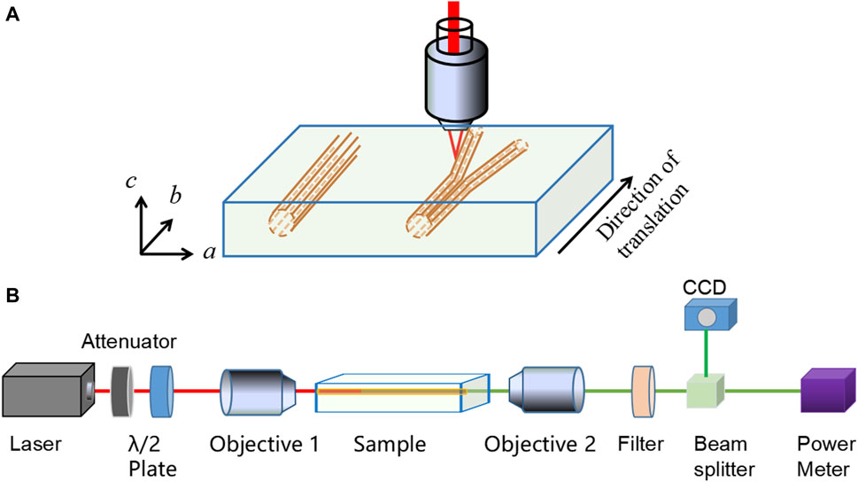
Figure 1. (A) Schematic plot of femtosecond laser direct writing in the KTP crystal. (B) Schematic of the end-face coupling system for SHG in cladding waveguides.
2.2 Optical waveguiding properties and SHG measurement
An optical microscope was used for a preliminary assessment of femtosecond laser-induced modifications. A typical end-face coupling optical system was used to characterize the transmission properties of the inscribed-cladding waveguides and splitters. A near-infrared (1,064 nm) laser was coupled to one end of the sample using an objective lens. Another microscope objective lens was used as the out coupler, through which the transmitted light was collected and imaged using a charge-coupled device camera. A half-wave plate was used to adjust the polarization of the input laser beam. The insertion loss of the waveguides was estimated by directly measuring the powers of the injected and output light through a power meter, which can be expressed as: α(dB) = −10log10(Pout/Pin), where Pout and Pin are the output and input laser powers, respectively. Notably, the insertion loss value included contributions from the Fresnel, coupling, and propagation losses. Thus, the propagation loss of the waveguide was less than the insertion loss.
This end-face coupling system was used for subsequent SHG measurements. Figure 1B shows a schematic of the end-face coupling system for SHG. A Q-switched solid-state laser with a central wavelength of 1,064 nm, pulse duration of 11 ns, and repetition rate of 5 kHz was used as the linearly polarized fundamental laser source for SHG excitation. The 1064-nm pulsed fundamental laser was coupled to the waveguide structures via an objective lens (×25, f = 5.5 mm). The 1064-nm fundamental and generated 532-nm green laser emitted from the output facet of the waveguides were collected using another ×25 microscope objective. Finally, the second harmonic (SH) light was separated from the residual fundamental laser using a filter with a transmittance of 98.5% at 532 nm and a reflectivity of >99% at 1,064 nm.
2.3 μ-Raman characterization
The laser damage tracks, waveguiding region, and bulk region of the crystal were characterized via μ-Raman spectroscopy using a confocal Raman microscopy system (LabRAM HR Evolution, HORIBA). A continuous-wave laser with a wavelength of 532 nm was used as the pump light source. A ×20 microscope objective (Olympus) was used to focus the 532-nm laser onto the waveguide end face and collect the generated vibration spectra.
3 Results and discussion
Figures 2A, B show the optical microscope cross-sectional images and measured near-field modal profiles of the fabricated straight-cladding waveguides. A fixed pulse energy of 600 nJ was used with a scan speed of 3.0 mm/s, horizontal polarized laser beam, and different depths of 45, 55, 65, 75, 80, and 85 μm. As shown in Figure 2A, when the depth was 85 μm, the inscribed tracks did not form the full circle. At other depths, the laser-induced damage tracks were clean, and no crystal cracking was observed, indicating well-defined circular claddings composed of distinct laser-induced tracks. As shown in Figure 2B, for depths of 45, 55, 65, and 75 μm, the waveguides exhibited good guiding confinement with extremely low light leakage outside the cladding volumes and multimode distribution. The insertion losses of these waveguides were 3.4, 3.1, 2.0, and 2.6 dB, respectively, as shown in the first row of Table 1. At a depth of 80 μm, a light leakage was observed at the bottom of the waveguide, and the insertion loss was 5.8 dB. At a depth of 85 μm, the guiding mode was not observed, which could be because at such a large depth the energy deposition decreased, leading to a less RI decrease in the inscribed tracks, which was not enough to construct a low-index potential-barrier wall to realize waveguiding.
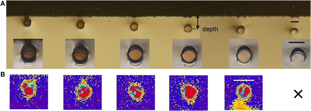
Figure 2. (A) Optical microscopic cross-sectional images. The insets show the enlarged microscopic images. (B) Measured near-field modal profiles of the straight-cladding waveguides inscribed with a pulse energy of 600 nJ, scan speed of 3.0 mm/s, horizontal polarization laser beam, and depths from 45 to 85 μm. Scale bars in all cases are 40 μm.
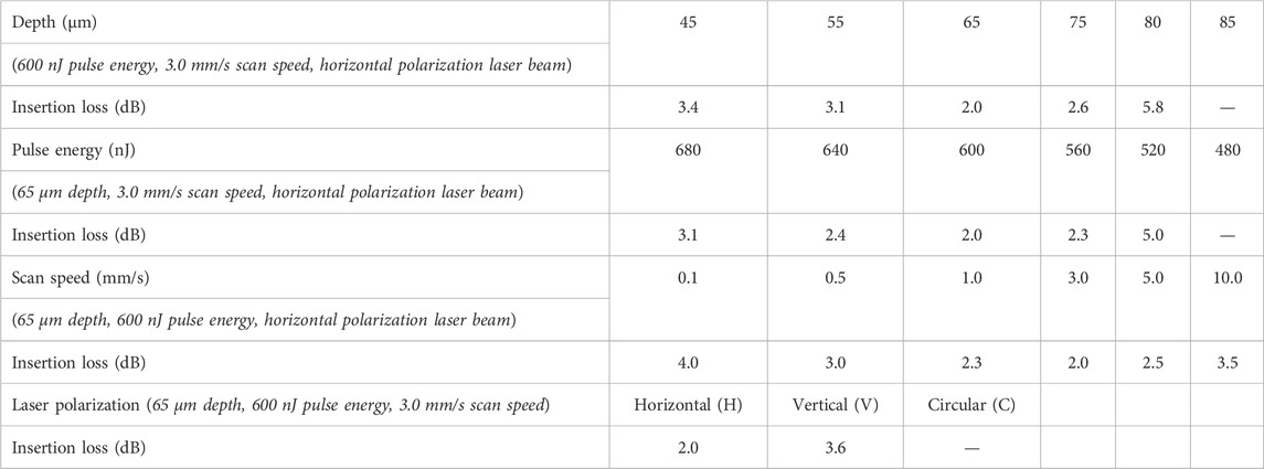
Table 1. Insertion losses of the straight-cladding waveguides fabricated with different inscription parameters.
The insertion losses of cladding waveguides fabricated with different inscription parameters are listed in Table 1. The second row of Table 1 shows the insertion losses of the waveguides fabricated at a depth of 65 μm, with a scan speed of 3.0 mm/s, horizontal polarization laser beam, and pulse energies from 480 to 680 nJ. The insertion loss was the smallest (∼2.0 dB) when the pulse energy was 600 nJ. The insertion loss increased as the pulse energy decreased from 600 to 520 nJ, which could be attributed to less energy deposition, causing a small RI decrease in the inscribed tracks, indicating an inferior light confinement effect. As the pulse energy was further decreased to 480 nJ, no guiding mode was observed. This might be because the decrease in the RI at the inscribed tracks was insufficient to construct a low-index potential barrier wall for waveguiding. When the pulse energy was increased from 600 to 680 nJ, the insertion loss increased, which was due to increased energy deposition, thereby affecting the region near the tracks and increasing the propagation loss. The third row of Table 1 shows the insertion losses of the waveguides fabricated at a depth of 65 μm, with a pulse energy of 600 nJ, horizontal polarization laser beam, and scan speeds from 0.1 to 10.0 mm/s. The smallest loss (∼2.0 dB) was observed when the scan speed was 3.0 mm/s. As the scan speed increased from 0.1–3 mm/s, the insertion loss progressively decreased. When the scan speed was increased from 3.0 to 10.0 mm/s, the insertion loss progressively increased. As shown in the fourth row of Table 1, the insertion loss strongly depended on the laser beam polarization. The insertion loss was the lowest for the waveguide inscribed with a horizontally polarized laser beam. In particular, optimal parameters to fabricate low loss waveguides are the focus depth of 55–75 μm, 560–680 nJ pulse energy, 0.5–5.0 mm/s scan speed, and horizontal polarization laser beam.
To investigate the polarization dependency of the waveguiding properties, all-angle optical transmission information at 1,064 nm of the straight-cladding waveguide (referred to as WG1) is presented in Figure 3. WG1 was fabricated with a pulse energy of 600 nJ, scan speed of 3.0 mm/s, depth of 65 μm, and a horizontal polarization laser beam. As the polarization of the excitation light at 1,064 nm changed from transverse-electric (TE; 0° and 180°) to transverse-magnetic (TM; 90° and 270°), the optical transmission varied from 27.1% to 62.5%, respectively. The insertion losses were 5.6 and 2.0 dB for the TE and TM polarizations, respectively. In comparison, the transmitted laser with TM polarization is better confined, which is attributable to the larger RI change induced by the femtosecond laser along the TM direction. The all-angle optical transmission information at 532 nm of the WG1 was also investigated. It was found that polarization dependency of the waveguiding at 532 nm were generally consistent with that at 1,064 nm.
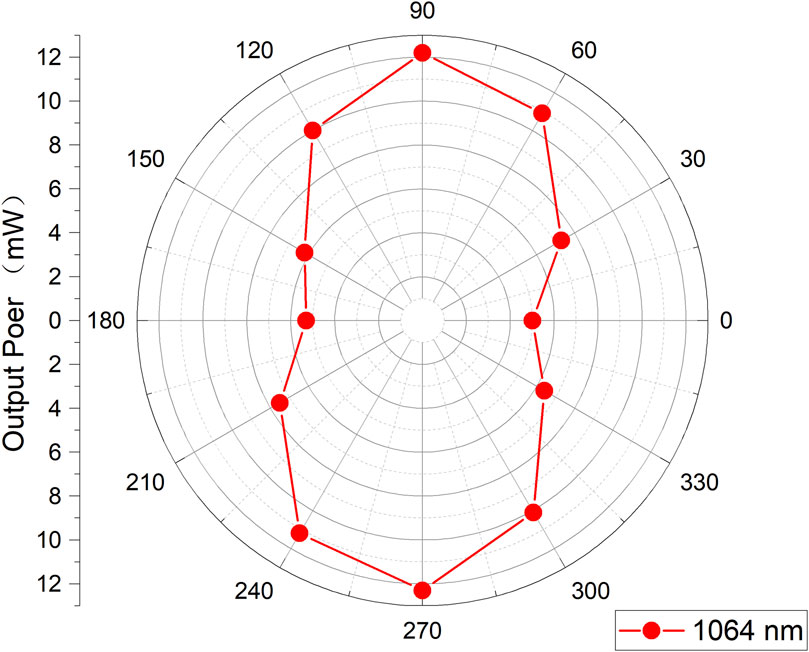
Figure 3. Optical transmission of the cladding waveguide WG1 at 1,064 nm along all-angle polarization.
The structure modification in the cladding was confirmed by μ-Raman spectroscopy. The μ-Raman results obtained from the output cross-section of cladding waveguide WG1 are presented in Figure 4. Figure 4A shows the μ-Raman emission spectra obtained for the bulk material, laser-induced track, and waveguide core. Three main phonon modes corresponding to the peaks of Raman shift at approximately 211.4, 267.4, and 693.0 cm−1 were measured. The spectra from the track and waveguide core had the same shape and peak positions as those in the bulk region. However, for the three Raman modes, the Raman peak intensity decreased at the laser-induced track and increased in the waveguide region. Similar results were obtained from the Raman intensity spatial mapping at the 693 cm−1 Raman mode shown in Figure 4B. For easy visualization, Figure 4C shows the one-dimensional (1D) distribution of the μ-Raman intensity measured along the blue dotted and magenta dashed lines in Figure 4B. Compared to the bulk region in the KTP, the Raman peak intensity at the laser-induced tracks decreased by approximately 26% on average, suggesting lattice distortion in the laser-induced region accompanied by an RI decrease [34]. Therefore, laser-induced tracks can be regarded as barriers that confine light inside the waveguides. However, the Raman peak intensity in the waveguide region increased by approximately 20%, indicating that the fabricated waveguides maintained the characteristically high Raman gain of the KTP crystal.
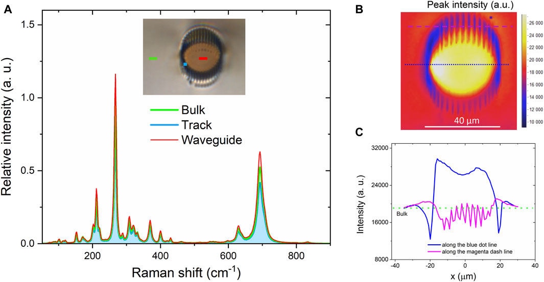
Figure 4. μ-Raman results obtained from the output cross-section of the KTP-cladding waveguide WG1. (A) μ-Raman emission spectra collected from the bulk material (green line), the waveguide core (red line), and the femtosecond laser-induced track (blue line). The insert shows the optical transmission micrograph of the cladding waveguide. (B) μ-Raman intensity spatial mapping at the 693 cm−1 Raman mode. (C) 1D distribution of the Raman intensity along the blue dotted and magenta dashed line of (B).
Figure 5A shows the typical emitted laser spectra of the fundamental (at 1,064 nm) and SH signals in WG1 using a 1064-nm pulsed laser pump. The peak SH wavelength was 532 nm, with a full width at half maximum of approximately 1 nm. Figure 5B shows the captured SH guiding modes along the TE and TM polarizations; the SH light was observed to be multimodal.
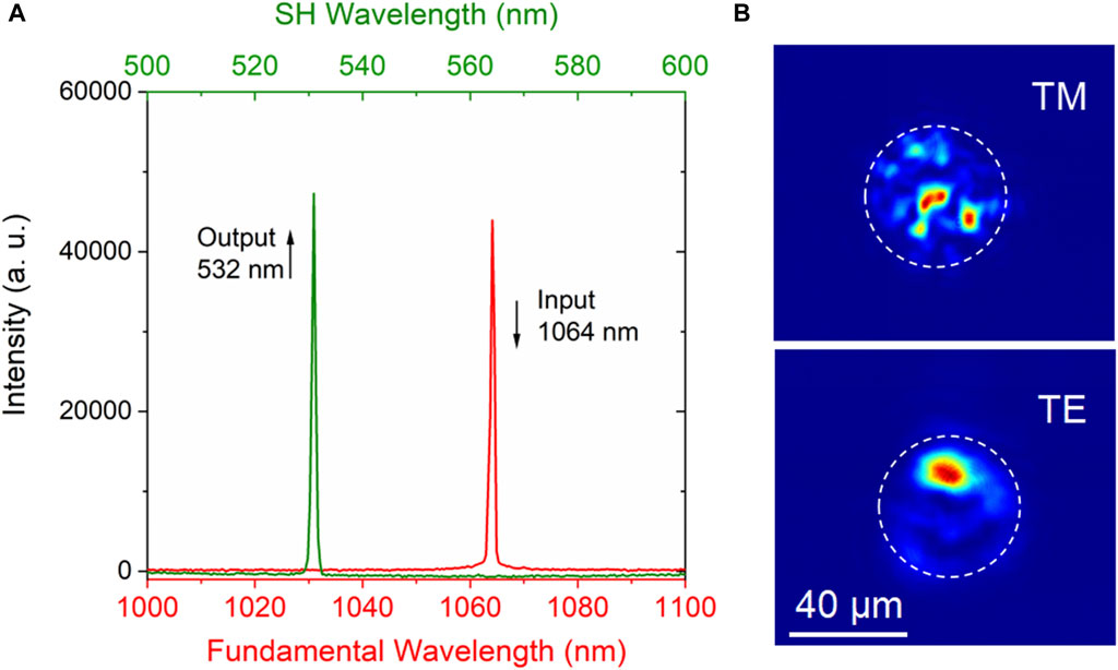
Figure 5. (A) Emitted laser spectra of the fundamental (red) and SH (green) waves, and (B) SHG modal profiles from the cladding waveguide WG1.
The generated SH power and conversion efficiency as functions of the input 1064-nm fundamental pump power are shown in Figure 6. As Figure 6A shows, while the excitation fundamental peak power reached 252.6 mW, the peak power of the generated SH light in WG1 reached 79.29 mW, corresponding to a peak conversion efficiency of ηpeak ≈ 31.4%. For comparison, the straight-cladding waveguide with a diameter of 24 μm (WG2), which was manufactured under the same conditions, had an insertion loss of 2.8 dB. This means that the loss increased in the waveguide as the diameter decreased. The reason may be that the smaller waveguide had a smaller acceptance angle and some high order modes were cut off leaving the near fundamental modes. As shown in Figures 6A, B maximum green laser output power of 33.75 mW was obtained, which corresponds to an SH conversion efficiency of ηpeak ≈ 13.3%. It can be concluded that with increased waveguide size, the straight-cladding waveguides possess lower insertion losses and exhibit better SHG performance.
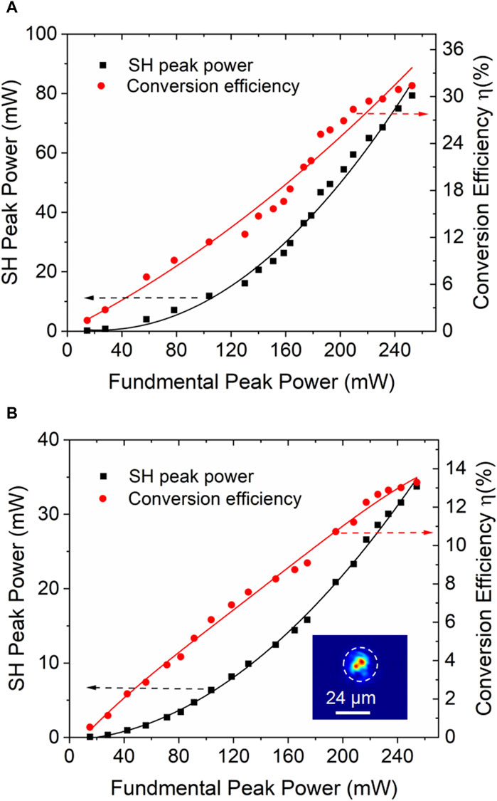
Figure 6. Measured SHG output power and conversion efficiency values as a function of 1064-nm fundamental peak power from (A) the WG1, and (B) the WG2. Inset is the TM modal profile at 532 nm. The solid lines represent the fit of the experimental data.
Y-branch waveguides capable of 1–2 beam splitting were fabricated with a pulse energy of 600 nJ, depth of 65 μm, and scan speed of 3.0 mm/s. The Y-branch splitters consisted of a 2.0-mm straight bus waveguide with a diameter of 48 μm, which was followed by two divergent identical waveguides with a diameter of 24 μm. The splitting angle θ between the two arms was set to 0.5°, 1.0°, 1.6°, 2.0°, and 2.6°, hereinafter referred to as Y1, Y2, Y3, Y4, and Y5, respectively. Figures 7A–C show the optical microscope images of the input, output, and top views of the Y-branch splitters Y1–Y5. As shown in Figure 7B, well-defined circular claddings composed of distinct laser-induced tracks acted as waveguide boundaries. Crystal cracking was observed in the output facets of Y3–Y5. Cracks propagated out of the laser-induced damaged region, thus allowing light propagation in the waveguide core. The distances between the two exiting ports of the Y-branch splitters Y1, Y2, Y3, Y4, and Y5 were 70, 116, 174, 213, and 268 μm, respectively. Figure 7C shows the details of the joint between the straight bus waveguide and the two split waveguides in each Y-branch splitter.
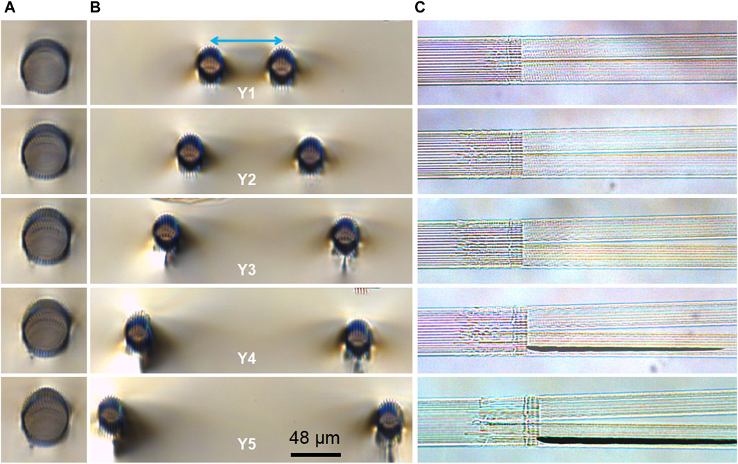
Figure 7. Optical microscope images of the cladding Y-branch waveguides Y1–Y5: (A) end view of the input facets, (B) end view of the output facets, and (C) top view.
Figure 8 illustrates the measured near-field modal profiles of the Y-branch splitters, Y1–Y5. All Y-branch splitters exhibited good splitting capability even with a large splitting angle of 2.6°, without high light leakage through the waveguide barrier or via the splitting point into the substrate regions. The output powers through each of the two arms of Y1 were measured, and a splitting ratio of 48.8:51.2 was achieved, indicating near equalization of the incident beams. Table 2 lists the splitting ratios and additional losses of the Y-branch splitters. The additional loss was estimated by comparing the total loss of the splitter with the insertion loss of the straightforward waveguide with a diameter of 48 μm. As the splitting angle increased from 0.5° to 2.6°, the splitting ratio decreased from 48.8:51.2 to 45.1:54.9. Y1 and Y2 exhibited low additional losses of 0.60 dB and 0.70 dB, respectively. As the splitting angle increased, the additional loss increased. For Y5, the additional loss increased to 2.5 dB.
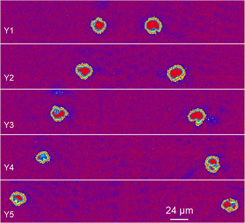
Figure 8. Measured near-field modal profiles along TM polarization of the cladding Y-branch waveguides Y1–Y5 at 1,064 nm.
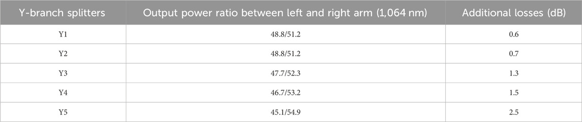
Table 2. Splitting ratios and additional losses of the Y-branch splitters.
The input laser beam excited both arms of the Y-branch waveguide to generate SH waves simultaneously. Figures 9A, B depict the generated SH wave powers and conversion efficiencies as functions of the input fundamental pump power at 1,064 nm from the Y-branch waveguide Y2, and the inset depicts the modal profile of SH light. The maximum peak power of the generated SH light in Y2 reached 33.63 mW from an input power of 251 mW, corresponding to a conversion efficiency of ηpeak ≈ 13.4%. The maximum SH peak power from the left and right arms of Y2 were 16.42 and 17.21 mW, respectively. The highest frequency conversion efficiency achieved from the left and right arms of Y2 were 6.54% and 6.85%, respectively. The SHG splitting ratio between the two arms in Y2 was approximately 48.8:51.2. The maximum output power of the SH light and the conversion efficiency of the Y-branch waveguides Y1 and Y3 are listed in Table 3. The differences in the SH output powers and conversion efficiencies collected from Y1–Y3 and the straight waveguide may be due to the splitting angles of the configurations and the effect of the Y-junction on the SHG performance.
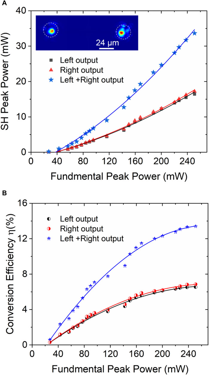
Figure 9. (A) Measured SHG output power and (B) conversion efficiency as a function of input fundamental peak power from the Y-branch waveguide Y2. The inset shows the modal profile at 532 nm.
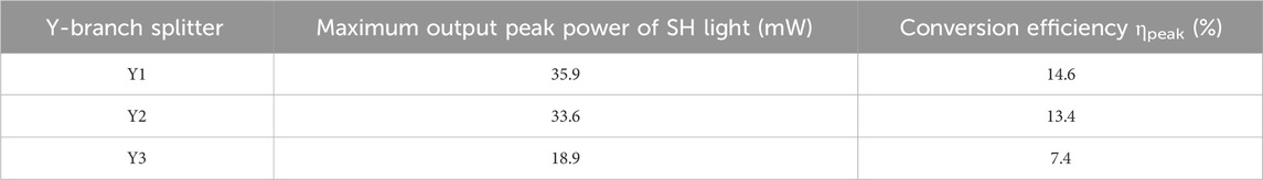
Table 3. SHG properties of the Y-branch waveguides.
Table 4 summarizes the SH performance (1,064→532 nm) and waveguiding properties of KTP waveguides achieved recently. Compared with the SHG performance of ion-irradiated KTP waveguides [11, 37], the maximum conversion efficiency was significantly higher for the cladding waveguides. The conversion efficiency in this study was comparable to the previously reported data for the KTP waveguides by femtosecond laser writing [19, 36].
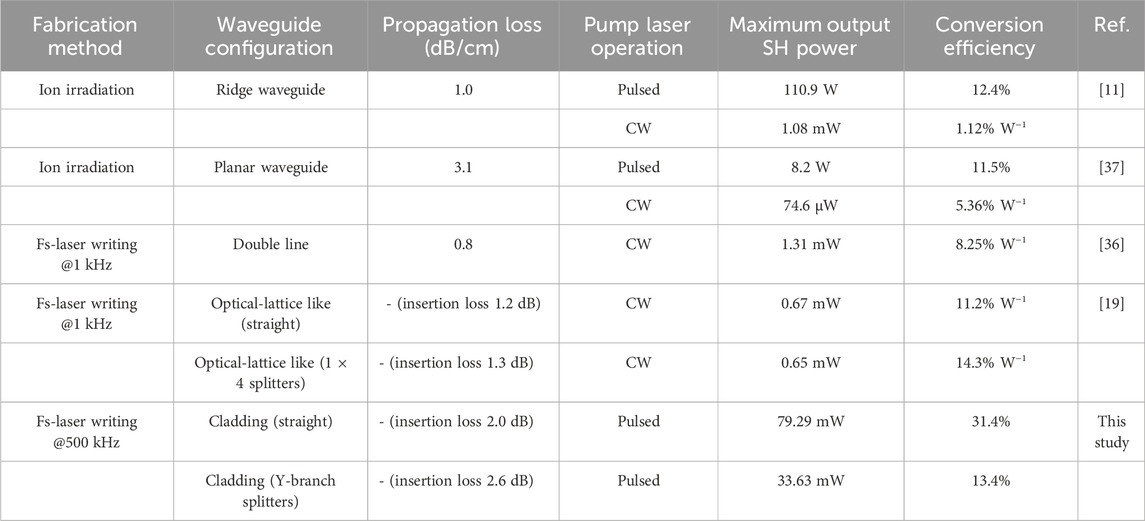
Table 4. Comparison about SH performance of KTP waveguides at ∼1 μm.
4 Conclusion
We fabricated straight depressed-cladding waveguides and Y-branch splitters with different splitting angles (0.5°, 1°, 1.6°, 2°, and 2.6°) in KTP crystals using femtosecond laser-direct writing. The fabricated waveguides exhibited good guiding properties with an insertion loss of 2.0 dB at 1,064 nm. The influence of the writing parameters on the quality of the cladding waveguides was studied. We found that optimal parameters to fabricate low loss waveguides are the focus depth of 55–75 μm, pulse energy of 560–680 nJ, scan speed of 0.5–5.0 mm/s, and a horizontal polarization laser beam. The Raman properties of the KTP crystal were explored using confocal μ-Raman spectroscopy. SHG at 532 nm from the KTP-cladding waveguides was demonstrated under 1064-nm pulsed laser pumping. The optical conversion efficiency of SHG was 31.4% with a maximum power of 79.29 mW in the straight-cladding waveguide. Y-branch waveguide splitters were based on depressed-cladding waveguides with a circular cross-section featuring a single Y-junction and a nearly symmetrical shape. At a small angle (0.5°), the splitter exhibited an additional loss as low as 0.60 dB compared to a straight waveguide. For a larger angle (2.6°), the additional loss increased to 2.5 dB. These splitters exhibited strong light confinement and nearly equal output powers. The Y-branch waveguide with a splitting angle of 1.0° generated a maximum SH output power of 33.63 mW and an SH efficiency of 13.4%. Overall, the results achieved in this study are promising for the fabrication of more complex photonic microstructures based on dielectric crystals, such as interferometers, waveguides with multiple Y-branches, or 3D bulk/surface structures. Beam-splitter-type waveguides providing multiple frequency doubling output signals from a single pump could be used in quantum optics, optical sensing, and communication applications. The Y-branch waveguide with an output channel separation of 174 μm also makes devices such as power dividers, frequency converters, and optical switches suitable for efficient connection to optical fibers.
Data availability statement
The original contributions presented in the study are included in the article/Supplementary Material, further inquiries can be directed to the corresponding author.
Author contributions
S-LL: Writing–original draft, Writing–review and editing. YS: Data curation, Writing–review and editing. L-NM: Formal Analysis, Writing–review and editing. H-LW: Formal Analysis, Writing–review and editing.
Funding
The author(s) declare that financial support was received for the research, authorship, and/or publication of this article. The work is supported by National Natural Science Foundation of China (NSFC) (Nos 61205055 and 12205167).
Acknowledgments
The authors acknowledge A. K. Kar and Dr. M. Mackenzie from Heriot-Watt University for their assistance with the experiments of femtosecond laser direct writing, and G. Li and T. Fang from Shandong University for SHG characterization.
Conflict of interest
The authors declare that the research was conducted in the absence of any commercial or financial relationships that could be construed as a potential conflict of interest.
Publisher’s note
All claims expressed in this article are solely those of the authors and do not necessarily represent those of their affiliated organizations, or those of the publisher, the editors and the reviewers. Any product that may be evaluated in this article, or claim that may be made by its manufacturer, is not guaranteed or endorsed by the publisher.
References
1. Marshall GD, Politi A, Matthews JCF, Dekker P, Ams M, Withford MJ, et al. Laser written waveguide photonic quantum circuits. Opt Express (2009) 17:12546–54. doi:10.1364/OE.17.012546
2. Bogaerts W, Taillaert D, Luyssaert B, Dumon P, Campenhout JV, Bienstman P, et al. Basic structures for photonic integrated circuits in silicon-on-insulator. Opt Express (2004) 12:1583–91. doi:10.1364/OPEX.12.001583
3. Chen F, de Aldana JRV. Optical waveguides in crystalline dielectric materials produced by femtosecond-laser micromachining. Laser Photon Rev. (2014) 8(2):251–75. doi:10.1002/lpor.201300025
4. Li L, Kong W, Chen F. Femtosecond laser-inscribed optical waveguides in dielectric crystals: a concise review and recent advances. Adv Photon (2022) 4(2):024002. doi:10.1117/1.AP.4.2.024002
5. Zhang B, Wang L, Chen F. Recent advances in femtosecond laser processing of LiNbO3 crystals for photonic applications. Laser Photon Rev (2020) 14(8):1900407. doi:10.1002/lpor.201900407
6. Burghoffff J, Nolte S, Tünnermann A. Origins of waveguiding in femtosecond laser-structured LiNbO3. Appl Phys A (2007) 89(1):127–32. doi:10.1007/s00339-007-4152-0
7. Gross S, Withford MJ. Ultrafast-laser-inscribed 3D integrated photonics: challenges and emerging applications. Nanophotonics (2015) 4(3):332–52. doi:10.1515/nanoph-2015-0020
8. Tang H, Lin XF, Feng Z, Chen JY, Gao J, Sun K, et al. Experimental two-dimensional quantum walk on a photonic chip. Sci Adv (2018) 4(5):eaat3174. doi:10.1126/sciadv.aat3174
9. Yuan T, Zhu B, Tu H, Chen Y, Chen X. Femtosecond laser direct writing quasi-phase matched type-II waveguide in lithium niobate. Opt Mater Express (2023) 13:1–8. doi:10.1364/OME.477618
10. Li G, Xu H, Yao Y, Jia Y, Chen F. Second harmonic generation in precisely diced KTiOAsO4 ridge waveguides. Opt Mater (2021) 121:111561. doi:10.1016/j.optmat.2021.111561
11. Chen C, Rüter CE, Volk MF, Chen C, Shang Z, Lu Q, et al. Second harmonic generation of diamond-blade diced KTiOPO4 ridge waveguides. Opt Express (2016) 24:16434–9. doi:10.1364/OE.24.016434
12. Thomas J, Heinrich M, Burghoffff J, Nolte S, Ancona A, Tünnermann A. Femtosecond laser-written quasi-phase-matched waveguides in lithium niobate. Appl Phys Lett (2007) 91(15):151108. doi:10.1063/1.2799178
13. Osellame R, Lobino M, Chiodo N, Marangoni M, Cerullo G, Ramponi R, et al. Femtosecond laser writing of waveguides in periodically poled lithium niobate preserving the nonlinear coefficient. Appl Phys Lett (2007) 90(24):241107. doi:10.1063/1.2748328
14. Chantakit T, Srinuanjan K, Yupapin PP. Two dimension photonic crystal Y-branch beam splitter with variation of splitting ratio based on hybrid defect controlled. Appl Phys A (2014) 117(2):547–52. doi:10.1007/s00339-014-8701-z
15. Paloczi GT, Huang Y, Yariv A, Luo J, Jen AKY. Replica molded electro-optic polymer Mach-Zehnder modulator. Appl Phys Lett (2004) 85(10):1662–4. doi:10.1063/1.1787944
16. Reshak AH, Shahimin MM, Khor KN, Wahid MHA, Hambali NA. Evanescent field optimization on Y-branch silicon nitride optical waveguide for biosensing. Mater Lett (2016) 173:127–30. doi:10.1016/j.matlet.2016.02.142
17. Liu HL, de Aldana JRV, Hong MH, Chen F. Femtosecond laser inscribed Y-branch waveguide in Nd:YAG crystal: fabrication and continuous-wave lasing. IEEE J Sel Top Quan Electron. (2016) 22(2):4500204. doi:10.1109/JSTQE.2015.2439191
18. Calmano T, Krankel C, Huber G. Laser oscillation in Yb:YAG waveguide beam-splitters with variable splitting ratio. Opt Lett (2015) 40(8):1753–6. doi:10.1364/OL.40.001753
19. Nie W, Jia YC, de Aldana JRV, Chen F. Efficient second harmonic generation in 3D nonlinear optical-lattice-like cladding waveguide splitters by femtosecond laser inscription. Sci Rep (2016) 6:22310. doi:10.1038/srep22310
20. Li SL, Ma LN. Y-branch waveguide splitters inscribed in Nd:KGW crystal by femtosecond laser writing: realization and laser emission. Opt Eng (2022) 61:047104. doi:10.1117/1.OE.61.4.047104
21. Chen F. Micro-and submicrometric waveguiding structures in optical crystals produced by ion beams for hotonic applications. Laser Photon Rev. (2012) 6(5):622–40. doi:10.1002/lpor.201100037
22. Oka T, Suhara T. Annealed proton-exchanged waveguide quasi-phase-matched second-harmonic generation devices in 8mol% MgO-doped congruent LiTaO3 crystal. Jpn J Appl Phys (2015) 54(10):100304. doi:10.7567/JJAP.54.100304
23. Suntsov S, Rüter CE, Kip D. Er:Ti:LiNbO3 ridge waveguide optical amplifiers by optical grade dicing and three-side Er and Ti indiffusion. Appl Phys B (2017) 123(4):118. doi:10.1007/s00340-016-6635-1
24. Gattass RR, Mazur E. Femtosecond laser micromachining in transparent materials. Nat Photon (2008) 2:219–25. doi:10.1038/nphoton.2008.47
25. Davis KM, Miura K, Sugimoto N, Hirao K. Writing waveguides in glass with a femtosecond laser. Opt Lett (1996) 21(21):1729–31. doi:10.1364/OL.21.001729
26. Tan D, Wang Z, Xu B, Qiu J. Photonic circuits written by femtosecond laser in glass: improved fabrication and recent progress in photonic devices. Adv Photon (2021) 3(2):024002. doi:10.1117/1.AP.3.2.024002
27. Imbrock J, Wesemann L, Kroesen S, Ayoub M, Denz C. Waveguide-integrated three-dimensional quasi-phase-matching structures. Optica (2020) 7(1):28–34. doi:10.1364/OPTICA.7.000028
28. Li SL, Huang ZP, Ye YK, Wang HL. Femtosecond laser inscribed cladding waveguide lasers in Nd∶LiYF4 crystals. Opt Laser Technol (2018) 102:247–53. doi:10.1016/j.optlastec.2018.01.003
29. Pätzold WM, Demircan A, Morgner U. Low-loss curved waveguides in polymers written with a femtosecond laser. Opt Express (2017) 25(1):263–70. doi:10.1364/OE.25.000263
30. Li SL, Ye YK, Wang HL. Cladding waveguide lasers in femtosecond laser written Nd:KGW waveguides. Opt Mater (2020) 110:110517. doi:10.1016/j.optmat.2020.110517
31. Ma LN, Li SL, Wang HL. Enhanced nonlinear optical properties of RGO via Au modification: application for Q-switched waveguide laser. Opt Mater Express (2021) 11:1583–159. doi:10.1364/OME.419432
32. Jia Y, de Aldana JRV, Romero C, Ren Y, Lu Q, Chen F. Femtosecond-laser-inscribed BiB3O6 nonlinear cladding waveguide for second-harmonic generation. Appl Phys Express (2012) 5(7):072701. doi:10.1143/APEX.5.072701
33. Yankov P, Schumov D, Nenov A, Monev A. Laser damage tests of large flux-grown KTiOPO4 crystals. Opt Lett (1993) 18(21):1771–3. doi:10.1364/OL.18.001771
34. Butt MA, Nguyen H, Ródenas A, Romero C, Moreno P, Vázquez de Aldana JR, et al. Low-repetition rate femtosecond laser writing of optical waveguides in KTP crystals: analysis of anisotropic refractive index changes. Opt Express (2015) 23:15343–55. doi:10.1364/OE.23.015343
35. Campbell S, Thomson RR, Hand DP, Kar AK, Reid DT, Canalias C, et al. Frequency-doubling in femtosecond laser inscribed periodically-poled potassium titanyl phosphate waveguides. Opt Express (2007) 15:17146–50. doi:10.1364/OE.15.017146
36. Laurell F, Calmano T, Müller S, Zeil P, Canalias C, Huber G. Laser-written waveguides in KTP for broadband Type II second harmonic generation. Opt Express (2012) 20:22308–13. doi:10.1364/OE.20.022308
Keywords: optical cladding waveguides, femtosecond laser writing, nonlinear optical materials, Y-branch waveguides, second harmonic generation
Citation: Li S-L, Song Y, Ma L-N and Wang H-L (2024) Femtosecond-laser-inscribed cladding waveguides in KTiOPO4 crystal for second-harmonic generation and Y-branch splitters. Front. Phys. 12:1341210. doi: 10.3389/fphy.2024.1341210
Received: 20 November 2023; Accepted: 01 May 2024;
Published: 13 May 2024.
Edited by:
Xinzhong Li, Henan University of Science and Technology, ChinaReviewed by:
Yingying Ren, Shandong Normal University, ChinaChaoliang Ding, Luoyang Normal University, China
Copyright © 2024 Li, Song, Ma and Wang. This is an open-access article distributed under the terms of the Creative Commons Attribution License (CC BY). The use, distribution or reproduction in other forums is permitted, provided the original author(s) and the copyright owner(s) are credited and that the original publication in this journal is cited, in accordance with accepted academic practice. No use, distribution or reproduction is permitted which does not comply with these terms.
*Correspondence: Shi-Ling Li, lishling@qfnu.edu.cn