Laser-induced damages to charge coupled devices with combined nanosecond/picosecond short-pulse lasers
 He Cao1,2† Xiaofan Xie1† Hao Chang3*
  Yunfei Li1,2* Jianfeng Yue1
  Yu Yu1,2*
  Gong Wang1,2 Ziqi Tang1 Lifang Li1
  Yulei Wang1,2 Zhiwei Lu1,2
- 1Center for Advanced Laser Technology, School of Electronics and Information Engineering, Hebei University of Technology, Tianjin, China
- 2Hebei Key Laboratory of Advanced Laser Technology and Equipment, Tianjin, China
- 3Department of Aerospace and Technology, Space Engineering University, Beijing, China
The research on laser induced breakdown mechanism of charge coupled devices (CCDs) brings new insights into photoelectric countermeasures. So far combined laser irradiation has been proved to be a more effective measure to destroy CCD. Due to the limitation of short-pulse laser combination method, the mechanism of CCD damage caused by combined short-pulse laser remains unexplored. Here, the distribution of temperature and stress field during the interaction between a combined short-pulse laser and a CCD is analyzed. A nanosecond/picosecond combined short-pulse laser system based on Stimulated Brillouin Scattering (SBS) pulse compression technique is designed. The damage threshold (DT) and properties of CCD by combined laser irradiation are characterized. The results show that the complete DT of combined laser induced CCD breakdown is only 103 mJ/cm2, which is only 44% of that of picosecond laser. The main cause of combined short-pulse laser induced CCD breakdown is short circuit (SC) between silicon substrate and silicon electrode.
1 Introduction
As core parts of the photoelectric detection systems, CCDs are widely applied in detection, identification, recognition [1–4], because of their low noise, high resolution, and low power consumption. However, CCDs are extremely vulnerable to be damaged due to their high detection sensitivity, which makes them be the primary targets for radiation source. Destroying the opponent’s detection systems and protecting own optoelectronic equipment are of strategic significance in optoelectronic countermeasures. A variety of CCD radiation sources have been reported, including X-ray [5–8]and plasma [9, 10] in recent years. Compared to these radiation sources, laser has the advantages of high brightness, small divergence angle, narrow wavelength range, long distance transmission. Laser can switch pulse output mode during irradiation, with good controllability, and is a kind of radiation source widely used to induce CCD breakdown. The laser-induced damages on CCDs mainly include the following three steps: CCD temperature rise, heat conduction, and thermal expansion. Specifically, the thermal stress increases with the raised temperature, which makes the internal structure of CCD constantly destroyed, and eventually leads to the complete failure. There has been shown that the induced breakdown effect of pulsed laser on photovoltaic devices is obviously stronger than that of continuous laser [11]. Furthermore, the damage effect of the combined laser is more significant than that of a single continuous laser or pulsed laser, due to that the combined laser can improve the coupling efficiency of the material to the laser, which is more conducive to damage to the materials and optical devices.
The research work of pulsed laser induced breakdown CCD is mostly based on long-pulse laser, due to the complexity of pulsed laser combination and the lack of reasonable theoretical model. In 2017, Zhong [12] used a combined millisecond/nanosecond laser to irradiate monocrystalline silicon and discovered the temperature rise of crystal was relatively slow with the enhancement of millisecond laser power density. In 2018, Zhang [13] established a damage model of silicon substrate induced by combined continuous/pulse laser. It was found that combined laser could make a stronger damage to silicon substrate by comparing the breakdown results of substrate. In the same year, by researching the damage mechanism of silicon materials caused by nanosecond and millisecond combined laser, it was found that the fusion DT of silicon was significantly reduced by combined pulsed laser irradiation, and the damage mechanism of combined pulsed laser on silicon materials was closely related to the thermal effect of millisecond pulsed laser and the thermal damage effect of nanosecond pulsed laser [14, 15]. In 2021, Xia [16] studied the damage mechanism of fused quartz under combined millisecond/nanosecond laser irradiation, and proposed that the combined millisecond and nanosecond pulsed laser can improve the thermal stress damage efficiency of laser irradiated fused quartz, which is caused by thermal effect and thermal stress effect. It is easy to find that the most used laser compound mode is the combination of millisecond laser and nanosecond laser, and there is no research related to nanosecond/picosecond short pulse combination laser irradiation CCD at present.
Compared with the combined millisecond/nanosecond laser, the superposition of picosecond and nanosecond short pulses makes peak power nonlinear sharp rise, and has a higher instantaneous temperature rise intensity. The material expands and cracks under the action of stress, and then produces serious damage in the longitudinal direction of the silicon substrate. Accordingly, the nanosecond/picosecond combined laser can effectively reduce the DT of CCD. However, it is difficult to realize the research of nanosecond/picosecond laser induced breakdown of CCD, due to the complexity of nanosecond and picosecond laser combination, and no reasonable theoretical model for the combined short-pulse laser induced CCD breakdown. Consequently, the key technology of short-pulse combined laser enhanced induced breakdown of CCD in photoelectric countermeasures system needs to be further studied.
In this paper, the SBS pulse compression technique is used to compress the nanosecond pulse into picosecond pulse at first, and the nanosecond pulse and picosecond pulse are combined by polarization beam combination and optical path compensation. Then the damage mechanism of the CCD irradiated by the nanosecond/picosecond combined laser is explained: the combination laser destroys the insulation layer between the silicon substrate and the silicon electrode, resulting in the failure of the clock line between the silicon electrode responsible for controlling signal transmission in a large area in a short time. Finally, the characteristics of combined laser and single laser induced CCD breakdown are compared. The complete DT of CCD under combined laser irradiation is only 103 mJ/cm2, which is far less than the complete DT under single picosecond laser (233 mJ/cm2) or single nanosecond laser (567 mJ/cm2) irradiation.
2 Principles and methods
2.1 Thermal stress distribution
When the CCD is irradiated by a short-pulse laser, its photosensitive region absorbs the laser energy and converts it into heat. Herein, the laser acting as a heat source; while the photosensitive region is heated in stages. Specifically, the heat absorbed by the photosensitive region is diffused in the form of heat conduction. Due to the difference of thermal conductivity, the materials inside CCD demonstrate distinctive temperature field distribution and thermal expansion, which generates different thermal stress distribution [17].
In metal or plasma, the thermal equilibrium time between electrons is about femtosecond magnitude, which is much less than the time that electrons and ions exchange energy. Therefore, the main mechanism of the interaction between nanosecond/picosecond combined short-pulse lasers and CCDs is still thermal damage. Here, we derive the thermal stress distribution equation of CCD under the irradiation of short-pulse as in Eq. (1). We assume that the laser energy distribution is uniform and the laser is vertically incident on the target surface; while the material is uniform and isotropic.
Where
2.2 Experimental setup
A nanosecond/picosecond combined short-pulse laser system (shown in Figure 1) was designed based on SBS pulse compression technique, polarization beam combination, and optical path compensation. Stable nanosecond/picosecond combined laser output could be achieved in this system. The P-state polarized laser (1064nm, 13ns) was divided into a P-state polarized laser and an S-state polarized laser by a half-wave plate and a polarization beam splitter (PBS). The P-state polarized laser was compressed through the SBS medium pool to obtain the circular-polarized laser with a wavelength of 1,064 nm and a pulse width of 841.5 ps. The corresponding circular-polarized laser was transformed into a S-state polarized laser by the quarter-wave plate. The SBS medium pool could couple the pump pulse to the stokes pulse front edge. The energy of the pump was absorbed by the stokes, resulting in a rapid increase in peak power and pulse compression. The uncompressed S-state polarized laser changed to P-state polarized laser by a half-wave plate. The P-state polarized nanosecond laser and S-state polarized picosecond laser were combined with PBS. The delay between the two laser beams were accurately regulated by adjusting the optical path between the two beams, to ensure that the picosecond laser was triggered at the center of the nanosecond laser pulse width. Moreover, the laser energy was precisely controlled by an energy regulator consisting of a half wave plate and a polarizer.
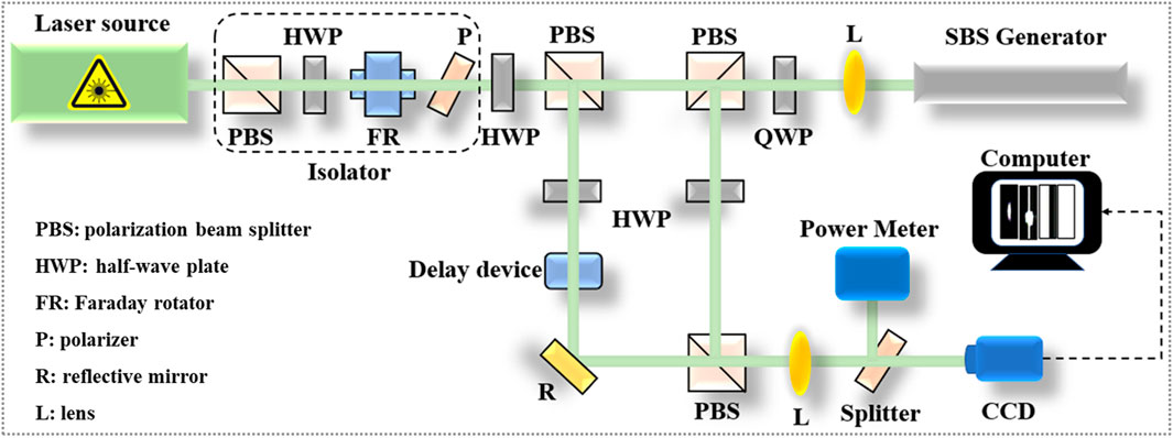
Figure 1. Combined nanosecond/picosecond laser path diagram.
3 Results and discussion
3.1 Theoretical simulation of combined laser-induced CCD breakdown
During the CCDs are irradiated by laser, the silicon substrate absorbs the energy of the focused laser and conducts heat to the surrounding area. When the laser is focused on the silica insulation layer between the silicon electrode and the silicon substrate, the ablation of the silica insulation layer generates a leakage current from the silicon electrode to the silicon substrate. After the insulation layer is completely ablated, the silicon electrodes on both sides of the focal point are short-circuited, which makes the clock confused and completely ineffective [18]. In general, the complete failure of CCD mainly attribute to the following two reasons [19, 20]: the SC between silicon substrate and silicon electrode or the SC between silicon electrodes. In order to investigate the main reasons of combined laser induced CCD damage, we simulate the distribution of stress field and temperature field of CCD in a certain irradiation time, and obtain the expansion degree of transverse and longitudinal regions under different energy densities. Our group has reported numerical simulations of single nanosecond laser and picosecond laser-induced CCD breakdown in previous work, which can work as control groups to elaborate the breakdown effect of combined laser-induced on CCD [21].
The finite element analysis method is used to obtain the thermal stress and temperature distribution as shown in Figures 2A,B. The distribution stress of and temperature field is not uniform inside the CCD. The maximum values of stress and temperature occur on the upper surface of the substrate, and the energy is diffused to the periphery over time. Due to the low thermal conductivity of the silica insulating layer, the heat is difficult to transfer through the insulation layer to the periphery in the silicon substrate. Figures 2C,D show the axial and radial temperature rise rules of laser focus. Nanosecond laser first begins to interact with CCD at Circle 1, and the temperature of CCD begins to rise slowly. Then the picosecond laser pulse reaches the silicon substrate at Circle 2, and the temperature inside the CCD rises sharply in a very short time with the action of combined nanosecond and picosecond lasers. The effect of the picosecond laser pulse ends at 5 ns (Circle 3), at which point the temperature begins to drop sharply until 7 ns. After 7 ns the temperature starts to drop slowly. Until the effect of nanosecond laser pulse ends (Circle 4), the effect of combined laser on CCD is completed. Finally, the CCD gradually returns to room temperature.
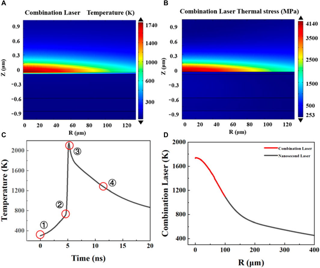
Figure 2. (A) The temperature field distribution of CCD irradiated by combined laser; (B) The stress field distribution of CCD irradiated by combined laser; (C) The change of temperature rises over time at the focal point of axial focus; (D) The change of temperature rises at the radial focal point.
The spot radius of nanosecond laser and picosecond laser are been set to 400 μm and 100 μm, and the start temperature of the model is 300 K. The influence region of combined laser is located at 0–100 μm in the radial direction; while the influence region of nanosecond laser is located at 100–400 μm as shown in Figure 2D. The temperature rise effect of combined laser on CCD is significantly stronger than that of single nanosecond laser, Combined laser can cause a sharp longitudinal temperature rise in a very short time. At 400 μm, the radial temperature drops to 350 K, and the temperature conducts to the region beyond 400 μm. This indicates that the damage caused by combined laser to CCD gradually diffuses from the focusing center point to the periphery. The temperature rises and stress caused by combined laser are much stronger than the effect of single nanosecond laser or picosecond laser. Therefore, combined nanosecond/picosecond laser brings stronger damage effect with less energy when interacting with CCD, which sharply reduces the threshold of damage to CCD.
3.2 Experiment study of laser-induced CCD breakdown
The model of CCD chip selected in the experiment is SONY-ICX811AL. The wavelength of nanosecond and picosecond laser is 1,064 nm, and the pulse widths are 13 ns and 841.5 ps, respectively. The laser output mode is adjusted to single pulse output. The energy is gradually adjusted from low to high. The beam is focused on the leftmost position of CCD through the three-dimensional displacement platform. Each pulse is adjusted a distance to the right to eliminate the cumulative effect of multiple pulses and keep measurement result correct. Above experimental results are shown in Figure 3.
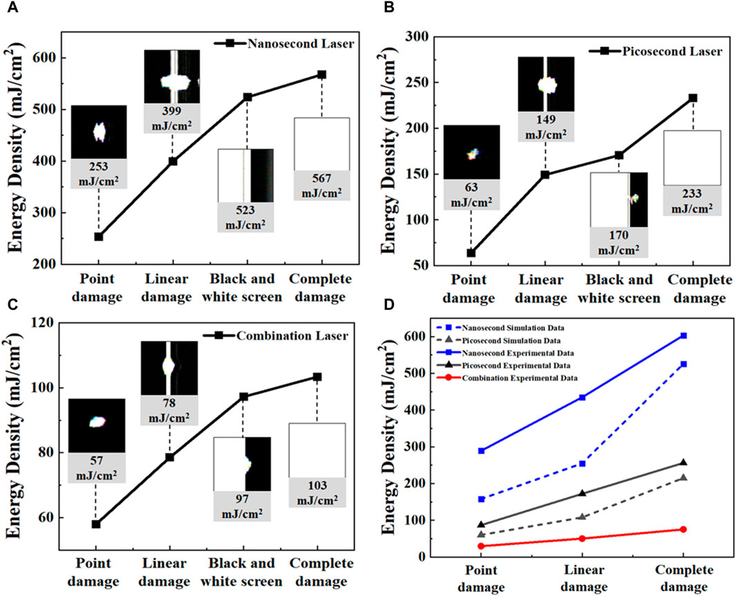
Figure 3. Damage image and functional DT of CCD irradiated by (A) nanosecond laser; (B) picosecond laser; (C) combined laser. (D) Comparison of experimental results and simulation results of CCD induced breakdown threshold caused by short-pulse laser.
As the laser energy increases, four stages of damage are observed: point damage, line damage, black and white screen, and complete damage [21]. Table 1 shows the DTs corresponding to the four damage stages. Compared with nanosecond laser, picosecond laser is vulnerable to cause the initial damage to CCD with higher peak power and narrower pulse width. The DT at each stage is obviously below that of nanosecond laser. Compared with nanosecond laser, the DT of CCD under combined laser irradiation is reduced by about 3–4 times. Compared with picosecond laser, the initial point damage threshold of combined laser on CCD is slightly lower. However, the threshold of complete damage caused by combined laser is only 44% of that of picosecond laser and 18% of that of nanosecond laser, which indicates that combined laser is easier to cause complete CCD failure than single nanosecond laser or picosecond laser. Compared with single nanosecond laser or picosecond laser, the combined laser can make the internal temperature rise of CCD more drastic, which can result in greater stress difference and cause more serious damage.
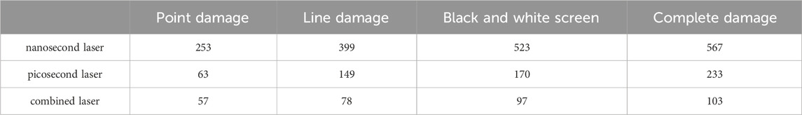
Table 1. Thresholds of CCD induced breakdown effect induced by short-pulse lasers (mJ/cm2).
The DT obtained by the simulation is lower than the experimental results since the simulation process is established in an ideal condition, which ignores the dynamic changes of the loss of the beam in the propagation process and the material properties with the internal temperature rise. But the change of the threshold in every stage is consistent, indicating that the model of the interaction between CCD and pulsed laser is reasonable. It can be employed to predict the DT of the interaction between short-pulse laser and different materials, which is of great significance for the future photoelectric countermeasure equipment.
So as to study the damage mechanism of CDD caused by combined laser, the morphologies of CCDs are investigated by scanning electron microscope, as shown in Figure 4. Unlike the CCD irradiated by the single nanosecond laser or picosecond laser, the damage pit of the interaction between the combined laser and the CCD can be clearly observed without removing the microlens layer, as shown in Figure 4A. In the area outside the damage pit, the microlens layers are still neatly arranged on the surface, as shown in Figure 4B, which indicates that the combined laser irradiation produces stronger thermal effect. The energy and thermal stress diffusion reaches a deeper longitudinal distance. In addition, many residual silicon electrodes can be observed in the central area of the damage pit. After removing the microlens, thickened layer and silicon nitride layer on the surface layer, the silicon electrodes present a complete arrangement under the protection of tungsten shielding. However, the residual silicon electrodes in the central area of the damage pit are seriously damaged and can hardly maintain a complete morphology, as shown in Figures 4C,D. Since the spot size and pulse width of picosecond laser are smaller than that of nanosecond laser, the damage effect at the edge is equivalent to that when the CCD is irradiated by single nanosecond laser. The insulation layer and silicon substrate below the silicon electrode have been severely damaged; while small damage pits have appeared as shown in Figure 4F. It indicates that when the CCD is irradiated with combined laser, the silicon substrate instantly absorbs the energy at the laser focus and generates a large amount of heat. The drastic temperature rise in a short period of time changes the material properties, resulting in an extremely strong stress that damages the silicon substrate from the inside out to the microlens layer.
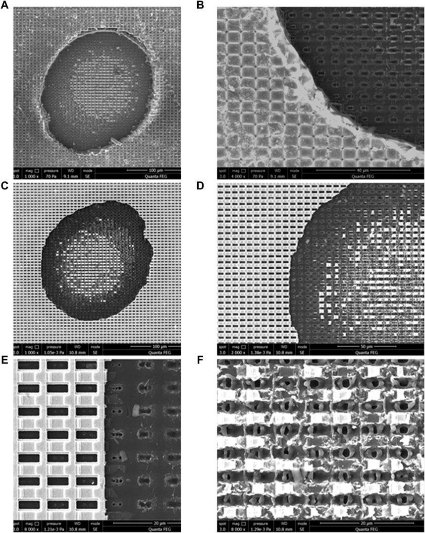
Figure 4. (A) Damage morphology in the area of interaction between combined laser and CCD; (B) Enlarged image of the boundary area of the damage pit; (C) Damage pit appearance after removing microlens layer; (D) Enlarged image of damage pit edge in figure C; (E) Morphology of silicon electrode and silicon substrate at the edge of damage pit; (F) Morphology of residual silicon substrate and silicon electrode in the central area of damage pit. The energy density of the combined laser is 105 mJ/cm2 and the spot diameter of the combined laser is 500 µm.
After removing the blackout metal tungsten at the edge of the damage pit, the silicon electrode below can be observed as shown in Figure 5A. Although the blackout tungsten covering the silicon electrode is not damaged, the silicon electrode below is fractured to varying degrees. The above phenomenon indicates that the damage of CCD caused by combined laser also starts from the inside. After magnification of the intact silicon electrode outside the edge of the damage pit, it is found that the insulation layer below has been broken down, as shown in Figure 5B. After further removing the electrode, the morphology of the insulation layer is observed as shown in Figure 5C. The morphology of the area near the damage center is shown on the left side of the picture. After magnification of the central area of the irradiation point, it can be found that the insulation layer has been completely ablated, and irregular small damage pits are shown on the silicon substrate, as shown in Figure 5D. The longitudinal temperature rise caused by the combination laser irradiation of CCD is extremely strong, which is enough to destroy the insulation layer and lead to the SC between silicon electrode and silicon substrate.
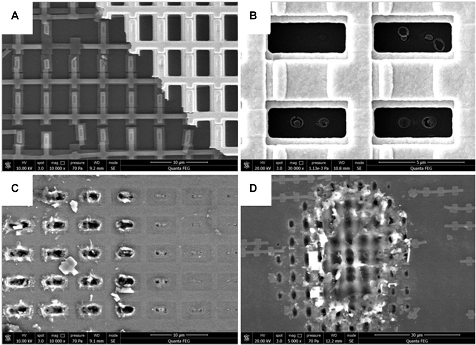
Figure 5. (A) Morphology of the damaged silicon electrode; (B) Morphology of intact silicon electrode in the boundary region of damage pit; (C) Morphology of the damaged silica insulation layer; (D) Morphology of silicon substrate in the central area of damage pit.
4 Conclusion
In this paper, we demonstrate the breakdown mechanisms and morphological features of CCD with combined nanosecond/picosecond laser. Compared with the irradiation of single laser, the combined laser can destroy CCD a lower energy. Moreover, the intensity of temperature rises and diffusion ranges during combined laser irradiation are much greater than that of single nanosecond or picosecond laser. Through observing the morphology of damaged CCD layer by layer, it is confirmed that the SC between silicon substrate and electrode is the main cause of CCD breakdown induced by combined laser. In addition, the fundamental reason for the breakdown of CCD by combined short-pulse laser is thermal effect. Combined laser destroys the insulation layer between silicon substrate and silicon electrode, resulting in a large area of failure of the clock line between silicon electrode which is responsible for controlling signal transmission in a short time. This work provides theoretical basis and technical support for the development of laser countermeasure equipment.
Data availability statement
The original contributions presented in the study are included in the article/Supplementary Material, further inquiries can be directed to the corresponding authors.
Author contributions
HC: Investigation, Writing–original draft. XX: Investigation, Writing–original draft. HC: Data curation, Writing–review and editing. YuL: Data curation, Writing–review and editing. JY: Software, Writing–review and editing. YY: Software, Writing–review and editing. GW: Visualization, Writing–review and editing. ZT: Visualization, Writing–review and editing. LL: Visualization, Writing–review and editing. YuW: Supervision, Validation, Writing–review and editing. ZL: Supervision, Validation, Writing–review and editing.
Funding
The author(s) declare that financial support was received for the research, authorship, and/or publication of this article. This work was supported by 173 project technical fund (JSLY-16-B16006), Key Laboratory Fund Project (Grant No.2021JCJQLB055004), National Natural Science Foundation of China (Grant No. 62004059, 62075056 and 62005074), Natural Science Research Foundation of Hebei University of Technology (JBKYXX2203), Natural Science Foundation of Hebei Province (Grant No. F2021202047, F2022202035 F2021202002), and Funding Projects for the Introduction of Overseas Staff of Hebei Province (Grant No. C20210334).
Conflict of interest
The authors declare that the research was conducted in the absence of any commercial or financial relationships that could be construed as a potential conflict of interest.
Publisher’s note
All claims expressed in this article are solely those of the authors and do not necessarily represent those of their affiliated organizations, or those of the publisher, the editors and the reviewers. Any product that may be evaluated in this article, or claim that may be made by its manufacturer, is not guaranteed or endorsed by the publisher.
References
1. Liu S, Chen X, Li Y, Cheng X. Micro-distortion detection of lidar scanning signals based on geometric analysis. Symmetry (2019) 11:1471. doi:10.3390/sym11121471
2. Bian Y, Xu W, Hu Y, Tao J, Kuang Y, Zhao C. Method to retrieve aerosol extinction profiles and aerosol scattering phase functions with a modified CCD laser atmospheric detection system. Opt express (2020) 28:6631–47. doi:10.1364/OL.42.004607
3. Gao J, Pan J, Wang J, Cai Y, Zhao Y. Triple charge-coupled device cameras combined backscatter lidar for retrieving PM2.5 from aerosol extinction coefficient. Appl Opt (2020) 59:10369–79. doi:10.1364/AO.405219
4. Wang Z, Tao Z, Liu D, Xie C, Wang Y. New technique for aerosol detection in haze day using side-scattering lidar and its inversion method. Earth Space Sci (2020) 7:7. doi:10.1029/2019EA000866
5. Peckerar MC, Baker WD, Nagel DJ. X-ray sensitivity of a charge-coupled-device array. J Appl Phys (1977) 48:2565–9. doi:10.1063/1.323974
6. Gopinath D, Soman M, Holland A, Keelan J, Hall D, Holland K, et al. Soft X-ray radiation damage in EM-CCDs used for resonant inelastic X-ray scattering. J Instrum (2018) 13:C02027. doi:10.1088/1748-0221/13/02/C02027
7. Blamires NG, Myatt J. X-Ray effects on pacemaker type circuits. Pacing Clin Electrophysiol (1982) 5:151–5. doi:10.1111/j.1540-8159.1982.tb02206.x
8. Chen Z, Shi K, Chen N, Shi L, Zhuang X, Zhou J, et al. The experimental study about laser-induced dizziness effect of medium-wave infrared seeker which based on image processing. J Vis Commun Image R (2019) 59:401–6. doi:10.1016/j.jvcir.2018.12.044
9. Dai Y, Song C, Lei J, Han Y, Gaoa X. Optical radiation characteristics of laser-induced air plasma and jamming CCD imaging detector. J Appl Spectrosc (2020) 87:387–92. doi:10.1007/s10812-020-01011-4
10. Carrère JP, Oddou JP, Place S, Richard C, Benoit D, Jenny C, et al. New mechanism of plasma induced damage on CMOS image sensor: analysis and process optimization. Solid-state Electron (2011) 65-66:51–6. doi:10.1016/j.sse.2011.06.037
11. Xu B, Yu H, Cheng K, Meng X, Wang J, Xu X, et al. Numerical simulation of thermal and mechanical damage in CCD detector induced by laser. In: Fifth International Symposium on Laser Interaction with Matter; November, 2018; Changsha, China (2018).
12. Zhong F, Lu X, Li J, Shen Z, Lu J, Ni X. Numerical analysis of thermal effect of the combined laser on single crystal silicon. Laser J (2017) 41:637–43.
13. Zhang M, Nie J, Sun K. Thermal function in silicon substrate of CCD induced by combined laser. In: Fifth International Symposium on Laser Interaction with Matter; October, 2019; Xi'an, China (2019).
14. Lu X. Research on the damage mechanisms of silicon materials irradiated by combined millisecond and nanosecond laser. Nanjing, China: Nanjing University of Science and Technology (2018).
15. Lu X, Li Z, Zhang J, Ni X. Surface damage study of silicon induced by combined millisecond and nanosecond laser with different delays. Laser J (2020) 44:695–9.
16. Xia S. Study on thermal stress of fused silica damage induced by millisecond-nanosecond combined pulse laser. Jilin, China: Changchun University of Science and Technology (2021).
17. Han M, Nie J, Sun K, Wang X, Dou X. Experiment on the temporal evolution characteristics of a CCD multilayer structure irradiated by a 106 μm continuous laser. Appl Opt (2018) 57:4415–20. doi:10.1364/ao.57.004415
18. Li M. Study on interference mechanism of visible CCD irradiated by 0.632 μm laser. Laser J (2020) 41:137–40.
19. Xu L, Cai H, Li C, Tan Y, Jin G, Zhang X. Degradation of responsivity for photodiodes under intense laser irradiation. Optik (2013) 124:225–8. doi:10.1016/j.ijleo.2011.11.055
20. Li M, Jin G, Tan Y, Guo M, Zhu P. Study on the mechanism of a charge-coupled device detector irradiated by millisecond pulse laser under functional loss. Appl Opt (2016) 55:1257–61. doi:10.1364/AO.55.001257
Keywords: charge coupled device, combined laser exposure, breakdown effect, photoelectric countermeasure, stimulated Brillouin scattering
Citation: Cao H, Xie X, Chang H, Li Y, Yue J, Yu Y, Wang G, Tang Z, Li L, Wang Y and Lu Z (2024) Laser-induced damages to charge coupled devices with combined nanosecond/picosecond short-pulse lasers. Front. Phys. 12:1345859. doi: 10.3389/fphy.2024.1345859
Received: 28 November 2023; Accepted: 26 March 2024;
Published: 10 April 2024.
Edited by:
Anna Cimmino, ELI Beamlines, CzechiaReviewed by:
Aleksėj Rodin, Center For Physical Sciences And Technology (CPST), LithuaniaYi Liu, Taiyuan University of Technology, China
Copyright © 2024 Cao, Xie, Chang, Li, Yue, Yu, Wang, Tang, Li, Wang and Lu. This is an open-access article distributed under the terms of the Creative Commons Attribution License (CC BY). The use, distribution or reproduction in other forums is permitted, provided the original author(s) and the copyright owner(s) are credited and that the original publication in this journal is cited, in accordance with accepted academic practice. No use, distribution or reproduction is permitted which does not comply with these terms.
*Correspondence: Hao Chang, changhao5976911@163.com; Yunfei Li, yfli@hebut.edu.cn; Yu Yu, yuyu1990@hebut.edu.cn
†These authors have contributed equally to this work and share first authorship