Ultra-broadband infrared metamaterial absorber based on MDMDM structure for optical sensing
 Fengjie Li1 Jiansen Du2 Shang Wang3 Ruitao Yu1 Xi Wang4 Tiqiang Zhang1 Zongtao Chi1
  Bin Wang1* Ning Li5*
- 1College of Electronic Information, Micro-Nano Technology College, Qingdao University, Qingdao, China
- 2Qingdao International Travel Healthcare Center, Qingdao, China
- 3College of Science, North China Institute of Science and Technology, Yanjiao, China
- 4China Tobacco Shandong Qingdao Tobacco Co., Ltd., Logistics Center, Qingdao, China
- 5School of Basic Medicine, Qingdao University, Qingdao, China
Infrared observation is a crucial tool in the study of astronomical celestial bodies. Metamaterials have a vast prospect for applications in the field of optics due to their unique electromagnetic tunable characteristics. In order to obtain an ultra-broadband high absorption material in the infrared region, we proposed a metal-dielectric-metal-dielectric-metal (MDMDM) metamaterial absorber using a titanium (Ti) nano-cross layer based on surface plasmon polariton (SPP) resonance and magnetic resonance cavity principles. The geometrical parameters of each layer have been examined carefully. The influence of incident angle from 0° to 60° is investigated for transverse electric and transverse magnetic plane-waves. Near-perfect absorption performance is achieved from near-infrared to mid-infrared region. The average absorption reaches as high as 97.41% from 2.05 to 6.08 μm. The absorber exhibits polarization-sensitive characteristics. The absorption peaks are 99.50% and 99.80% at 2.55 and 5.24 μm, respectively. The proposed material has potential applications in astronomical imaging, volcano and fire detection, remote sensing, biological monitoring, and other optical devices.
1 Introduction
Metamaterial perfect absorbers (MPAs) are composite artificial structures with enhanced electromagnetic properties that are difficult to achieve with natural materials. Unlike traditional absorbers that rely on intrinsic absorption with low efficiency, MPAs exhibit broadband and high absorption characteristics that can be adjusted by changing the dimensions and shapes of the absorbers. Infrared observation is an essential method in astronomical research (Jakobsen et al., 2022). Astronomical observations play a crucial role in the study of celestial bodies (Gao et al., 2023). Infrared observations are crucial for studying low-temperature environments, such as star-forming regions with multiple dusty star clouds and the satellites and icy surfaces of planets within them. Changes in the star-forming regions enveloped by gases and dust can be detected by measuring the infrared wavelength, providing insights into the ongoing processes (Hamilton et al., 2019). Utilizing the characteristics of metamaterials, broad-spectrum absorption in the infrared wavelength range can be achieved, holding significant importance for infrared astronomical observations.
MPAs have attracted significant attention due to their distinctive tunable properties. The development of nanotechnology has provided a greater range of metamaterial absorber applications. Landy et al. (2008) first proposed and implemented an experimental MPA in the microwave band. Subsequent research has resulted in the utilization of MPAs in various light wavebands: microwave (Zhang et al., 2019); ultraviolet (Zeng et al., 2021; Mehrabi et al., 2022; Takashima et al., 2022; Wang et al., 2022); visible (Yu et al, 2020a; Liu et al., 2020; Issah et al., 2021); infrared (Enoch et al., 2004; Wu et al, 2020a; Zhou et al., 2021; Shi et al., 2022; Wang et al., 2024); terahertz (Cong et al., 2015; Wang et al., 2019; Wu, 2020; Zheng et al., 2022). Due to the ultra-thin structure, broadband and high absorption capacities, MPAs have been widely used in imaging (Diem et al., 2009; Tittl et al., 2015; Zhang et al., 2024), sensing (Sabah et al., 2018), and solar energy collection (Yu et al, 2020b; Lin et al., 2020). Typical MPAs consist of a periodic array, a three-layer structure composed of metal-dielectric-metal (MDM). As a result of electromagnetic resonance, the high absorption shown by MDM occurs within a narrowband range (Cong et al., 2015). In recent years, researchers have been actively working to expand the bandwidth of absorbers. Arranging multi-shapes in the top layer represents a common approach to expanding bandwidth. Shobhit et al. proposed a metasurface solar absorber based on a Ge2Sb2Te5 (GST) substrate (Patel et al., 2022). They adopted a square and a circle as the top-level periodic structure with a resultant absorption above 90% from ultraviolet to near-infrared band regions. Liang et al. (2022) designed a 4-layer ultra-broadband absorber with a second-order Peano fractal curve (PFC) metasurface; the average absorption reached 94.3%, with wavelengths ranging from 12.3 to 32 μm (Liang et al., 2022). Zheng et al. (2022) proposed a three-layer structure absorber with a VO2 circular resonator, and explained the working principle in the basis of a distribution of the electric field. Following absorber optimization, the absorption was close to 100% at 3.7–9.7 THz. Due to resonance coupling of the horizontal plane, the bandwidth was greatly expanded. The design of a vertically-stacked resonator structure can enhance absorption. Wang et al. (2022) proposed an absorber integrated with metallic rings, where the associated average absorption exceeded 91% within the wavelength range 0.2–7 μm. Multilayer structures serve to expand the absorption bandwidth, as do the use of lumped-elements and plasmonic-nanocomposites.
The spectral band of the mentioned absorbers mainly focuses on terahertz, long-wave infrared, and visible light to near-infrared regions. There is currently limited reporting on wideband absorbers in the near-infrared to mid-infrared range. The near-infrared wideband absorption is not only applicable to environment detection (Wu et al, 2020b) but also can manage stray light and reduce interference. This is particularly crucial in optical communication systems, aiding in minimizing signal loss and maintaining signal integrity (Liu et al., 2022). The mid-infrared band is associated with thermal infrared remote sensing (Liu et al., 2021), infrared camouflage (Qin et al., 2022), and optical imaging (Zeng et al., 2018). The 2.50–5.00 μm range marks the beginning of the thermal infrared spectrum and is a crucial window for ground-based observations, encompassing the L and M bands. Multi-band infrared absorbers have a broader range of applications compared to single-band absorbers. However, achieving dual-band wideband high absorption poses a challenge due to the negative correlation between bandwidth and absorption rate. Li et al. (2022) designed a multi-layer nanorod structure to achieve full coverage absorption in the range of 3.00–5.00 μm. The absorption of their proposed absorber was only 86%. However, their research focuses only on the mid-infrared single band, and the absorption performance is relatively low. Wu et al. (2023) achieved an absorption efficiency of 93.5% in the 2.00–5.40 μm range by incorporating a metal (Ti) into the dielectric layer (Al2O3). The resultant absorber delivered excellent absorption performance from the near-infrared to the mid-infrared region, but the absorption rate still below 95%. In this study, we proposed an ultra-broadband metamaterial absorber consisting of a MDMDM (Ti-SiO2-Ti-SiO2-Ti) structure with a top-level periodic nano-cross shape. The absorption rate is 97.41% from 2.05 to 6.08 μm for light as a transverse electric (TE) plane-wave, with the wave perpendicular to the z direction and electrical field transmissions along the x direction. Moreover, Ti and SiO2 are sufficiently abundant to facilitate widespread manufacturing. As shown in Table 1, in comparison to previous research on near-infrared and mid-infrared absorbers, our proposed absorber not only achieves dual-band infrared absorption in the near-infrared and mid-infrared regions but also demonstrates a significant improvement in bandwidth and absorption rate.
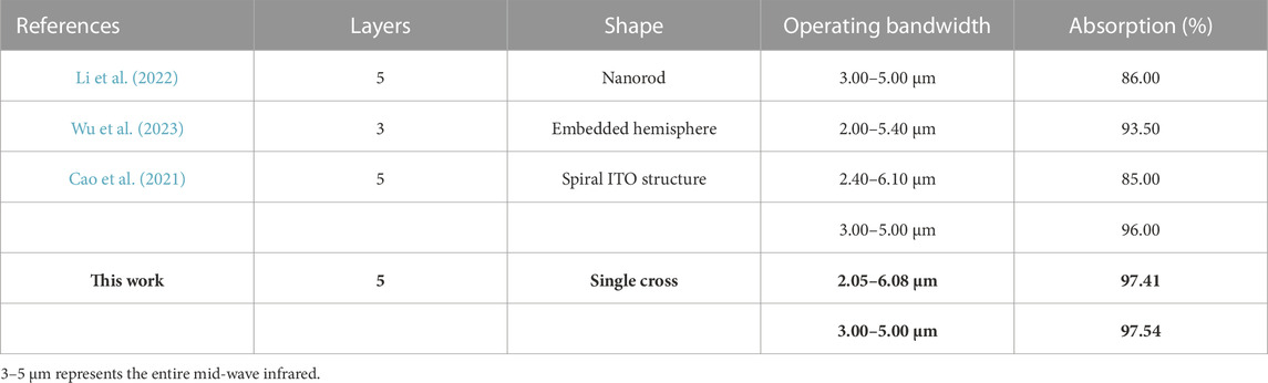
TABLE 1. Comparison of published studies on near-infrared and mid-infrared light absorbers with this work.
In Section 2, we introduced the detailed structure and materials of the proposed absorber. In Section 3, we analyzed the working principle of the absorber based on the impedance matching principle and surface plasmon resonance. The broadband absorption was analyzed by calculating the distribution of electromagnetic fields within the absorber. Multi-resonant coupling and multi-layer plasma resonance combine to extend bandwidth absorption. We investigated the impact of geometrical parameters on absorption performance. The polarization angle was studied. We also discussed the impact of various incident angles, from 0° to 60° for transverse electric (TE) polarized and transverse magnetic (TM) polarized light, on absorber performance. In Section 4, We made a conclusion.
2 Materials and methods
The structure of our proposed absorber is illustrated in Figure 1. The metamaterial absorber is composed of five layers. A Ti nano-cross structure appears on the top plane. The second layer is a SiO2 square column (equal length and width). The third layer is a Ti square column, the fourth layer is a SiO2 square column and the fifth layer is a Ti square column. Absorption can be represented by A = 1-T-R, where A, T, and R denote absorption, transmission, and reflection, respectively. The bottom metal layer is thick enough to prevent incident light from passing through the absorber. As the transmission is zero, absorption is given by A = 1−R.
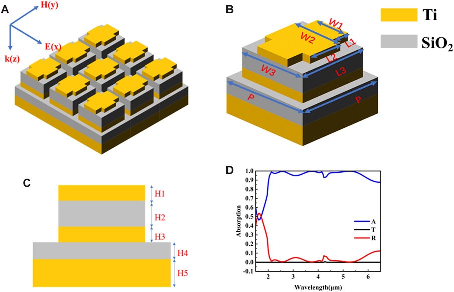
FIGURE 1. The structure and simulation results of proposed absorber. (A) The periodic array of the proposed absorber. (B) 3D view of the structural unit. (C) Side view of the structural unit. (D) The response of the proposed absorber with respect to absorption (A), transmission (T) and reflection (R) for TE-polarized light.
In addition to the structure, the constituent materials also significantly impact the absorption. Ti is a metallic component, and SiO2 serves as a dielectric material in our proposed absorber. In early research on the absorber, the metal layer employed high-Q factor noble metals (such as Ag and Au) resulting in excellent resonant selectivity within a specific wavelength range. The further development of absorber research incorporated other metals, including Ti, W, and Ni. In the near-infrared and mid-infrared regions, the imaginary permittivity of Ti contributes to broad absorption, improving absorptivity of the incident light and expanding the mid-infrared bandwidth. The incorporation of SiO2 as the dielectric layer enhances the performance of the absorber. An ultrathin SiO2 layer can realize broadband absorption at near-infrared and mid-infrared regions. Moreover, the permittivity of SiO2 exerts an influence on intrinsic absorption which combines with plasmon resonance, and improves broadband absorption. The permittivity of both Ti and SiO2 are taken from the handbook of Palik (Palik, 1997), as shown in Figure 2. The metamaterial absorber has been numerically simulated using the Finite-Difference Time-Domain (FDTD) method (Amedome Min-Dianey et al., 2019). In simulation calculations, the x-axis and y-axis boundaries were set periodically. Therefore, only a subunit calculation was required for photonic performance, which appreciably reduced the time and memory requirements. We used perfect-matched layers as a terminal condition for the z-axis which absorbed the incident electromagnetic field, equivalent to the field propagating unobstructed to infinity.
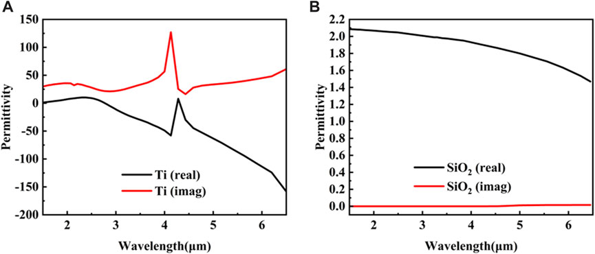
FIGURE 2. The permittivity values of materials (A) The permittivity values of Ti. (B) The permittivity values of SiO2.
The absorber is illuminated perpendicularly by light with TE polarization, which simulates plane waves with oblique incidence using the Broadband Fixed Angle Source Technique (BFAST). We perform material data curve fitting on the data to ensure they converge with the actual situation. For the simulation conditions, we chose a 10 nm × 10 nm × 10 nm mesh size. In order to fulfill the future fabrication process, the brief preparation technique is proposed. First, the bottom Ti and SiO2 films are deposited by physical vapor deposition (PVD) and plasma enhanced chemical vapor deposition (PECVD), respectively. Using the same PVD and PECVD deposition process, the middle Ti and SiO2 patterns are developed by high resolution photolithography. In the last step, the cross Ti pattern is made with PVD and PECVD deposition and photolithography. This fabrication process is relatively simple.
3 Results and discussion
Figure 1D shows the result of absorption performance. The average absorption reaches as high as 97.41% from 2.05 to 6.08 μm. The Controlled Variables method is made to find out the optimized parameters after a lot of work. The parameters of our proposed absorber are shown in Table 2. The impedance matching principle can explain the absorption result. The equivalent impedance (Z) can be extracted using the S-parameter inversion technique (Smith et al., 2002); S11 represents the reflecting parameter in Eq. 1, S21 represents the transmitted parameter in Eq. 2, and Z is the equivalent impedance in Eq. 3. The S parameter for the proposed absorber is shown in Figure 3A. Figure 3B illustrates the equivalent impedance of the absorber in the wavelength range 2.05–6.08 μm, where the real part is close to 1 and the imaginary part is close to 0. In accordance with the principle of impedance matching (Mehrabi et al., 2022), it can be inferred that the incident light experiences minimal reflection back into free space within the 2.05–6.08 μm wavelength range. We also conduct numerical calculations to validate the accuracy of the results.

TABLE 2. The parameter values of the absorber (μm).
FIGURE 3. Numerical Calculation of Equivalent Impedance (A) the S parameter value of the proposed absorber. (B) Equivalent impedance value of the absorber. (C) Numerical calculation of the reflection loss of the absorber. (D). Comparison of absorption between equivalent impedance calculation and simulation using the FDTD method.
Where Γ denotes the reflection coefficient in Eq. 4, Z0 denotes the normalized value of the free-space impedance (Z0 = 1), and RL represents the reflection loss in Eq. 5. Absorption (A) can be determined from the equivalent impedance calculations in Eq. 6. As illustrated in Figure 3C, in the wavelength interval spanning 2.05 to 6.08 μm, RL falls below −10 dB, signifying an absorption exceeding 90%. In Figure 3D, the simulation results for absorbance closely align with those derived from the equivalent impedance computations. The equivalent impedance treats the absorber as a unified entity, disregarding the specific contributions of individual layers. Consequently, this approach can lead to deviations between calculated and simulated outcomes. However, the two curves representing equivalent impedance calculation and simulation fit very well. This level of agreement serves as verification for the high absorption characteristics obtained from simulation.
The performance of absorbers has a bearing on the electromagnetic field. There are many free electrons in the metal that participate in collective resonance under the influence of the light wave electromagnetic field when light impinges on the inner surface of the metal and dielectric. Surface plasmon polariton (SPP) resonance can be excited when the oscillation frequency of free electrons couples with the incident light. It contributes to a strong absorption performance, and exhibits an enhanced electric field. The metal layer generates ohmic loss, converting the energy of the incident light to thermal energy for electron motion, which augments absorption performance. The metal-dielectric-metal absorber can be regarded as a magnetic resonance cavity composed of a closed magnetic wall. The upper and lower metal layers serve as parallel mirrors. The incident light is reflected by the lower metal when the light enters the absorber from the upper metal and then passes through the middle dielectric layer. The incident light from the upper layer interferes with the reflected light from the lower layer, forming a closed magnetic resonance cavity within the middle dielectric layer.
In order to elucidate the spectral absorption process, we analyzed the electromagnetic field distribution within the absorber corresponding to two absorption peaks. The incident light is a TE wave perpendicular to the z-axis, where the electromagnetic field distribution demonstrates the absorption principle presented in Figure 4. As depicted in Figures 4A, B for 2.55 μm, the electric field is present in proximity to both the upper and third Ti layer. This indicates that SPP resonance occurs in the metal-dielectric inner surface. There is a strong electric field in the y direction, indicating that the y direction of the nano-cross structure exhibits multi-resonant coupling. Figure 4C reveals a magnetic field enhancement in the magnetic resonance cavity of the second layer. This suggests that the first metal layer, the second dielectric layer, and the third metal layer form a closed magnetic resonance cavity. Multiple reflections and interferences of the incident light occur within the magnetic resonance cavity. The electrical loss of SPP resonance and the magnetic loss of the magnetic resonance cavity jointly serve to enhance absorption. The distribution of the electric field enhancement near the top layer of the Ti nano-cross structure for a 5.24 μm wavelength is shown in Figures 4D, E. There is an electric field enhancement, indicating multi-resonant coupling in the first layer. An electric-field enhancement also occurs in the third Ti layer. As illustrated in Figure 4F, the magnetic field is primarily confined at the boundary between the uppermost layer and the airspace above it, as well as between the second SiO2 dielectric layer and the third Ti layer. This suggests that the magnetic resonance cavity is no longer the primary contributor to absorption. At long wavelengths, local plasmon resonance caused by the top cross resonant structure contributes to absorption with an additional contribution due to the local plasmon resonance excited in the third layer.
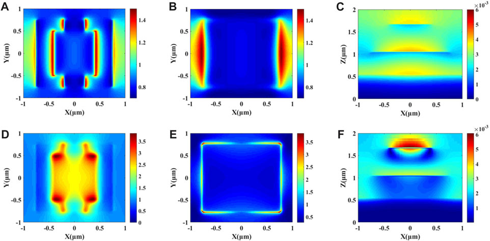
FIGURE 4. The electromagnetic field distribution at the absorption peaks. (A–C) the electromagnetic field distribution at 2.55 μm. (A) The electric-field distribution near the top-level nano-cross structure in the x-y plane. (B) The electric field distribution near the third Ti layer in the x-y plane. (C) The magnetic field distribution in the x-z plane. (D–F) The electromagnetic field distribution at 5.24 μm. (D) The electric field distribution near the top-level nano-cross structure in the x-y plane. (E) The electric field distribution near the third Ti layer in the x-y plane. (F) The magnetic field distribution in the x-z plane.
We discussed the impact of the structure and parameters on the absorption performance. As shown in Figure 5A, Case 1 is a traditional metal-dielectric-metal (MDM) three-layer absorber, where the average absorption reaches 73.27% within the wavelength range of 2.05–6.08 μm. Case 2 adds a SiO2 dielectric layer above the absorber, resulting in an average absorption of 78.67%. The added SiO2 is a loss dielectric that can undergo intrinsic absorption with a resultant slightly higher absorption compared to Case 1. Case 3 represents our proposed 5-layer nano-cross structure that exhibited an absorption of 97.41% in the infrared band, representing a significant improvement. The top-level nano-cross pattern leads to the excitation of multiple resonators and the generation of a new MDM magnetic resonance cavity. The additional resonant cavity and multiple resonators at the top layer contribute to the enhanced performance. Focusing on the nano-cross top layer, we investigated the influence of essential size parameters on absorption. We considered an increase in W2 from 0.42 to 1.22 in incremental 0.2 μm intervals. As shown in Figure 5B, the absorption increases with an increase in W2 from 0.42 to 0.82 μm within the wavelength range of 2.05–6.08 μm. The absorption is found to decrease when the W2 value increases from 0.82 to 1.22 μm. It indicates that an excessively high or low values of W2 weaken the resonant coupling of the top nano-cross structure and the surface plasmon resonance, lowering absorption. As shown in Figure 5C, an increase in L2 from 0.20 to 1.00 μm (in steps of 0.2 μm) is accompanied by an average absorption increase from 91.97% to 97.41%. An electric field enhancement occurs in the y direction of the top nano-cross structure, where surface plasmon resonance and resonator coupling are the main factors determining broadband absorption. The increase in L2 contributes to an enhanced electric field, in tandem with surface plasmon resonance and resonator coupling, resulting in improved absorption in the infrared band. The results presented in Figure 5D indicate that an increase in H1 from 15 to 55 nm (in steps of 10 nm) results in an average absorption decrease from 97.41% to 81.83%. Compared with L2 and W2, alterations in H1 exert a more substantial impact on absorption performance with a greater overall impact on the top-level nano-cross structure.
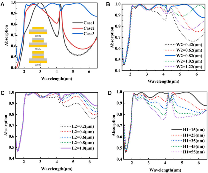
FIGURE 5. Influence of structure and parameters on absorption performance (A) absorption for the three structures. (B) Absorption where the width of the top Ti layer (W2) varies between 0.42 and 1.22 μm. (C) Absorption where the length of the top Ti layer (L2) varies between 0.2–1.0 μm. (D) Absorption where the height of the top Ti layer (H1) varies between 15 and 55 nm.
Other structural parameters also have a considerable effect on absorption. As shown in Figure 6A, an increase in H2 from 0.2 to 0.6 μm (in steps of 0.2 μm) serves to increase the average absorption from 87.05% to 97.41% within the wavelength range 2.05–6.08 μm. An additional rise from 0.6 to 1.0 μm results in a reduction in absorption to 85.61%. The change in H2 impacts on the phase of plane light entering the MDM resonant cavity, affecting the reflection interference. If H2 either is too large or too small, it weakens the effect of the resonant cavity, causing the incident light to reflect off the absorber with a consequent reduction in absorption. The change in H2 has an appreciable influence on absorption performance in wavelength range 2.05–6.08 μm. As shown in Figure 6B, following a change in H3 from 15 to 55 nm (in steps of 10 nm) within the wavelength range of 2.05–4.00 μm there is no major difference in absorption performance. Moreover, changes in H3 result in a negligible effect on absorption at 4.0–6.08 μm. Considering the distribution of electromagnetic fields, the third Ti layer mainly exhibits electric field enhancement at short wavelengths. At longer wavelengths, the surface plasmon resonance of the top Ti layer principally improves absorption performance with a small contribution from Ti in the third layer. The results presented in Figure 6C illustrate that an increase in H4 from 0.33 to 0.78 μm (in steps of 0.15 μm) mainly affects absorption within the wavelength 2.05–4.00 μm. An enhanced magnetic field in the fourth layer (SiO2) forms a magnetic resonance cavity but the enhancement gradually disappears with an increase in wavelength from 2.05 to 6.08 μm. The contribution of the fourth dielectric layer to absorption also gradually weakens. Through parameter analysis, we conclude that the resonator coupling of the top layer nano-cross structure contributes to absorption. The multi-layer structure generates multi-layer surface plasmon resonances and multiple magnetic resonance cavities that contribute to the broadband high absorption.
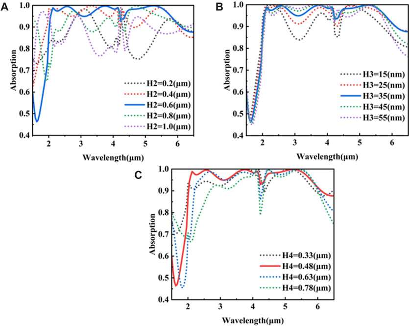
FIGURE 6. Impact of thickness on absorption performance (A) absorbance where the thickness of second SiO2 layer (H2) changes from 0.2 to 1.0 μm. (B) Absorbance where the thickness of third Ti layer (H3) changes from 15 to 55 nm. (C) Absorbance where the thickness of fourth Ti layer (H4) changes from 0.33 to 0.78 μm.
The absorption spectra where the polarization angle (φ) of the absorber is varied from 0° to 90° are presented in Figure 7. Absorption within the wavelength range 2.05–4.35 μm is minimally affected by variations in φ. The absorption spectrum is sensitive to φ in the range 4.30–6.08 μm. As the polarization angle increases from 0° to 90°, the average absorption within the infrared range decreases from 97.41% to 91.43%. This response that can be attributed to non-rotational symmetry, which impacts on the resonant coupling of the absorber. The wide-angle characteristic of absorbers is important in many practical applications. We have investigated the effect of angle on absorption in both TE and TM polarization modes. The absorption spectrum is presented in Figure 8 where the wavelengths ranged from 2.05 to 6.08 μm for TE and TM polarization with the incidence angle (θ) varying in 10° steps between 0° and 60°. As shown in Figures 8A, B, the average absorption decreases to 90.91% for a wavelength of 2.05–6.08 μm when θ is raised to 60° under TE polarization. The average absorption drops from 87.45% to 76.92% under TM polarization (Figures 8C, D) as θ is varied from 0° to 60° within the 2.05–6.08 μm wavelength band. The components of the electromagnetic field in various directions show significant changes due to the increase of incident angle. Enhancing the anisotropy of the incident light results in a more pronounced scattering of light (Mehrabi et al., 2022), which can account for the gradual decrease of absorption with an increase in θ. Our results demonstrate that the proposed absorber possesses wide-angle properties in the infrared region.
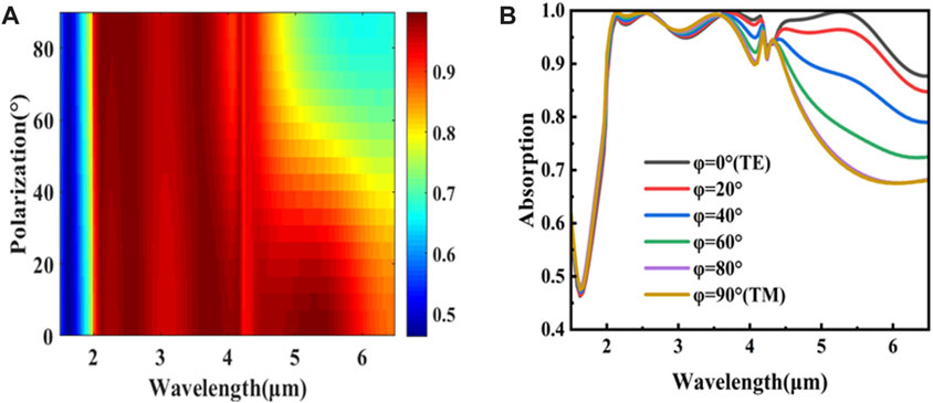
FIGURE 7. Influence of polarization angle on absorption performance (A,B) absorption at various polarization angles from 0° to 90°.
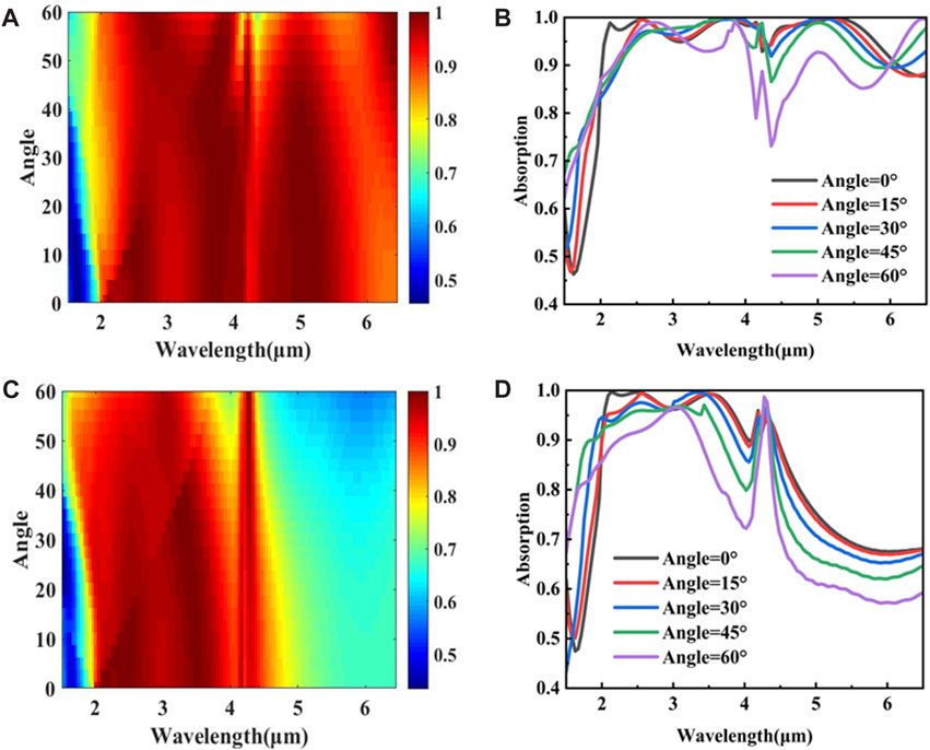
FIGURE 8. Impact of incidence angle on absorption performance (A,B) absorption at various angles for TE polarization modes. (C,D) Absorption at various angles for TM polarization modes.
4 Conclusion
An ultra-broadband metamaterial absorber with a Ti nano-cross layer is proposed. Both the horizontal and vertical structural elements contribute to the enhanced absorption exhibited by the proposed absorber. The absorber generates multiple effects that contribute to enhancing the absorption of incident light. The absorption mechanism has been revealed through an analysis of the electromagnetic field distribution. The effects of SPP resonance and the magnetic resonance cavity contribute to an ultra-broadband absorption from 2.05 to 6.08 μm. We have demonstrated how the multi-layer structure affects absorption and have considered the role of geometrical parameters. The level of absorption decreases from 97.41% to 90.22% in the case of TE polarized incident light varying from 0° to 60° in the infrared region. The average absorption drops from 87.45% to 76.92% when varying θ from 0° to 60° at 2.05–6.08 μm under TM polarization. We have combined the advantages of horizontal multi-resonators and vertically stacked structures to broaden the absorption bandwidth. The proposed absorber possesses a simple nano-cross structure on the top layer and a total of only five layers. Our proposed absorber demonstrates remarkable absorption performance in the infrared region, making it applicable to various optical devices, including infrared imaging and celestial body observation in astronomy.
Data availability statement
The original contributions presented in the study are included in the article/Supplementary Material, further inquiries can be directed to the corresponding authors.
Author contributions
FL: Investigation, Writing–original draft, Writing–review and editing. JD: Software, Writing–review and editing. SW: Methodology, Writing–review and editing. RY: Data curation, Writing–review and editing. XW: Validation, Writing–review and editing. TZ: Writing–review and editing. ZC: Project administration, Writing–review and editing. BW: Visualization, Writing–original draft, Writing–review and editing. NL: Writing–review and editing.
Funding
The author(s) declare financial support was received for the research, authorship, and/or publication of this article. This work was supported by the Qingdao Postdoctoral Application Research Project, the Chinese Ministry of Education’s Industry School Cooperation Collaborative Education project: 220606513074515, and the National Key Research and Development Program of China (2022YFC2302800).
Conflict of interest
Author XW was employed by China Tobacco Shandong Qingdao Tobacco Co., Ltd., Logistics Center.
The remaining authors declare that the research was conducted in the absence of any commercial or financial relationships that could be construed as a potential conflict of interest.
Publisher’s note
All claims expressed in this article are solely those of the authors and do not necessarily represent those of their affiliated organizations, or those of the publisher, the editors and the reviewers. Any product that may be evaluated in this article, or claim that may be made by its manufacturer, is not guaranteed or endorsed by the publisher.
Supplementary material
The Supplementary Material for this article can be found online at: http://www.frontiersin.org/articles/10.3389/fspas.2023.1338284/full#supplementary-material
References
Amedome Min-Dianey, K. A., Sanogo, D., M'Bouana, N. L. P., and Zhang, H. C. (2019). Angular dependence in light propagation through silver material based ultra-compact photonic crystal. Opt. Mater. 91, 1–6. doi:10.1016/j.optmat.2019.03.002
Cao, B. W., Li, C., Shi, W. J., Han, C. Q., Wu, Y., and Yan, C. C. (2021). Large-area mid-infrared broadband absorbers based on spiral ITO resulting from the combination of two different broadening absorption methods. Opt. Express 29, 34427–34440. doi:10.1364/OE.440535
Cong, L., Tan, S., Yahiaoui, R., Yan, F., Zhang, W., and Singh, R. (2015). Experimental demonstration of ultrasensitive sensing with terahertz metamaterial absorbers: a comparison with the metasurfaces. Appl. Phys. Lett. 106. doi:10.1063/1.4906109
Diem, M., Koschny, T., and Soukoulis, C. M. (2009). Wide-angle perfect absorber/thermal emitter in the terahertz regime. Phys. Rev. B 79, 033101. doi:10.1103/PhysRevB.79.033101
Enoch, S., Quidant, R., and Badenes, G. (2004). Optical sensing based on plasmon coupling in nanoparticle arrays. Opt. Express 15, 3422–3427. doi:10.1364/OPEX.12.003422
Gao, J. J., Wang, H. R., Zuo, Y. X., Yang, J., Chen, X. P., Zhang, M. Z., et al. (2023). Modeling and analysis of the active surface system for the large single-dish sub-mm telescope. IEEE Trans. Antennas Propag. 71, 225–235. doi:10.1109/TAP.2022.3218746
Hamilton, V. E., Simon, A. A., Christensen, P. R., Reuter, D. C., Clark, B. E., Barucci, M. A., et al. (2019). Evidence for widespread hydrated minerals on asteroid. Bennu 4, 332–340. 101955. doi:10.1038/s41550-019-0722-2
Issah, I., Li, F., Baah, M., Otoo, I. A., Asilevi, L., Bawuah, P., et al. (2021). Passive tunable and polarization-insensitive fan-like metamaterial absorber in the visible spectrum. J. Opt. Soc. Am. B 38, C1. doi:10.1364/josab.426441
Jakobsen, P., Ferruit, P., Alves de Oliveira, C., Arribas, S., Bagnasco, G., Barho, R., et al. (2022). The near-infrared spectrograph (NIRSpec) on the james webb space telescope I. Overview of the instrument and its capabilities. Astronomy Astrophysics 661, A80. doi:10.1051/0004-6361/202142663
Landy, N. I., Sajuyigbe, S., Mock, J. J., Smith, D. R., and Padilla, W. J. (2008). Perfect metamaterial absorber. Phys. Rev. Lett. 100, 207402. doi:10.1103/PhysRevLett.100.207402
Li, L., Cui, Q., Zhang, Y. J., Wu, Y., Han, C. Q., and Yan, C. C. (2022). Visible transparent mid-infrared broadband absorbers based on gradient refractive indexes and multi-size cavity resonances. Opt. Express 30, 43078–43087. doi:10.1364/OE.473986
Liang, Y., Liu, X., Xin, J., Zhang, X., Wang, Y., and Song, Y. (2022). Ultra-broadband long-wave infrared metasurface absorber based on Peano fractal curve. Results Phys. 33, 105169. doi:10.1016/j.rinp.2021.105169
Lin, K. T., Lin, H., Yang, T., and Jia, B. (2020). Structured graphene metamaterial selective absorbers for high efficiency and omnidirectional solar thermal energy conversion. Nat. Commun. 11, 1389. doi:10.1038/s41467-020-15116-z
Liu, J., Ma, W. Z., Chen, W., Chen, Y. S., Deng, X. C., and Gu, Y. (2021). A metamaterial absorber based on particle swarm optimization suitable for earth's atmospheric transparency window. IEEE Access 9, 92941–92951. doi:10.1109/ACCESS.2021.3089895
Liu, J., Ma, W. Z., Chen, W., Yu, G. X., Chen, Y. S., Deng, X. C., et al. (2020). Numerical analysis of an ultra-wideband metamaterial absorber with high absorptivity from visible light to near-infrared. Opt. Express 28, 23748–23760. doi:10.1364/OE.399198
Liu, W. J., Xiong, X. L., Liu, M. L., Xing, X. W., Chen, H. L., Ye, H., et al. (2022). Bi4Br4-based saturable absorber with robustness at high power for ultrafast photonic device. Appl. Phys. Lett. 120, 5. doi:10.1063/5.0077148
Mehrabi, S., Bilal, R. M. H., Naveed, M. A., and Ali, M. M. (2022). Ultra-broadband nanostructured metamaterial absorber based on stacked square-layers of TiN/TiO2. Opt. Mater. Express 12, 2199. doi:10.1364/ome.459766
Patel, S. K., Parmar, J., Katkar, V., Al-Zahrani, F. A., and Ahmed, K. (2022). Ultra-broadband and polarization-insensitive metasurface absorber with behavior prediction using machine learning. Alexandria Eng. J. 61, 10379–10393. doi:10.1016/j.aej.2022.03.080
Qin, Z., Zhang, C., Liang, Z. Z., Meng, D. J., Shi, X. Y., and Yang, F. M. (2022). Thin multispectral camouflage absorber based on metasurfaces with wide infrared radiative cooling window. Adv. Photonics Res. 3, 5. doi:10.1002/adpr.202100215
Sabah, C., Mulla, B., Altan, H., and Ozyuzer, L. (2018). Cross-like terahertz metamaterial absorber for sensing applications. Pramana-Journal Phys. 2, 17. doi:10.1007/s12043-018-1591-4
Shi, X., Hou, E., Liang, Z., Zhang, S., Dai, R., Xin, W., et al. (2022). Broadband metamaterial absorber based on hybrid multi-mode resonance in mid-wave and long-wave infrared region. Results Phys. 42, 105972. doi:10.1016/j.rinp.2022.105972
Smith, D. R., Schultz, S., Markoš, P., and Soukoulis, C. M. (2002). Determination of effective permittivity and permeability of metamaterials from reflection and transmission coefficients. Phys. Rev. B 65, 195104. doi:10.1103/PhysRevB.65.195104
Takashima, Y., Nagamatsu, K., Haraguchi, M., and Naoi, Y. (2022). Ultra-thin deep ultraviolet perfect absorber using an Al/TiO(2)/AlN system. Opt. Express 30, 44229–44239. doi:10.1364/OE.474847
Tittl, A., Michel, A. K., Schaferling, M., Yin, X., Gholipour, B., Cui, L., et al. (2015). A switchable mid-infrared plasmonic perfect absorber with multispectral thermal imaging capability. Adv. Mater 27, 4597–4603. doi:10.1002/adma.201502023
Wang, B., Ma, C., Yu, P., Govorov, A. O., Xu, H., Wang, W., et al. (2022). Ultra-broadband nanowire metamaterial absorber. Photonics Res. 10, 2718. doi:10.1364/prj.473332
Wang, B. X., Tang, C., Niu, Q., He, Y., and Chen, T. (2019). Design of narrow discrete distances of dual-/triple-band terahertz metamaterial absorbers. Nanoscale Res. Lett. 14, 64. doi:10.1186/s11671-019-2876-3
Wang, S., Du, J., Chi, Z., Coong, H., and Wang, B. (2024). Ultra-broadband metamaterial absorber in the far infrared. Mater. Lett. 355, 135518. doi:10.1016/j.matlet.2023.135518
Wu, B., Liu, Z., Du, G., Chen, Q., Liu, X., Fu, G., et al. (2020b). Polarization and angle insensitive ultra-broadband mid-infrared perfect absorber. Phys. Lett. A 384, 126288. doi:10.1016/j.physleta.2020.126288
Wu, J. (2020). A polarization insensitive dual-band tunable graphene absorber at the THz frequency. Phys. Lett. A 384, 126890. doi:10.1016/j.physleta.2020.126890
Wu, P. H., Wang, Y. Y., Yi, Z., Huang, Z., Xu, Z. S., and Jiang, P. P. (2020a). A near-infrared multi-band perfect absorber based on 1D gold grating fabry-perot structure. IEEE Access 8, 72742–72748. doi:10.1109/ACCESS.2020.2983394
Wu, Z., Liang, Z., Shi, X., Yang, F., Dai, R., Hou, E., et al. (2023). Broadband and energy-concentrated absorber based on hemispherical-embedded structure. Adv. Photonics Res. 4. doi:10.1002/adpr.202200301
Yu, P., Yang, H., Chen, X., Yi, Z., Yao, W., Chen, J., et al. (2020b). Ultra-wideband solar absorber based on refractory titanium metal. Renew. Energy 158, 227–235. doi:10.1016/j.renene.2020.05.142
Yu, Y., Yu, Z., and Sun, X. (2020a). Nonmetallic broadband visible-light absorbers with polarization and incident angle insensitivity. IEEE Photonics J. 12, 1–7. doi:10.1109/jphot.2020.3029213
Zeng, B. B., Huang, Z. Q., Singh, A., Yao, Y., Azad, A. K., Mohite, A. D., et al. (2018). Hybrid graphene metasurfaces for high-speed mid-infrared light modulation and single-pixel imaging. Light. Sci. Appl. 7, 51. doi:10.1038/s41377-018-0055-4
Zeng, L., Zhang, X., Ye, H., Dong, H., and Zhang, H. (2021). Design of ultra-broadband absorption enhancement in plasmonic absorber by interaction resonance of multi-plasmon modes and Fabry-Perot mode. Opt. Express 29, 29228–29241. doi:10.1364/OE.440172
Zhang, H. B., Du, J. S., Chi, Z. T., Cong, H. L., and Wang, B. (2024). Numerical design of a dual-wavelength confocal metalens with photonic crystal filter based on filter-substrate-metasurface structure. Opt. Commun. 554, 130157. doi:10.1016/j.optcom.2023.130157
Zhang, K. L., Zhang, J. Y., Hou, Z. L., Bi, S., and Zhao, Q. L. (2019). Multifunctional broadband microwave absorption of flexible graphene composites. Carbon 141, 608–617. doi:10.1016/j.carbon.2018.10.024
Zheng, Z., Luo, Y., Yang, H., Yi, Z., Zhang, J., Song, Q., et al. (2022). Thermal tuning of terahertz metamaterial absorber properties based on VO(2). Phys. Chem. Chem. Phys. 24, 8846–8853. doi:10.1039/d2cp01070d
Keywords: metamaterials, broadband, absorber, infrared, imaging
Citation: Li F, Du J, Wang S, Yu R, Wang X, Zhang T, Chi Z, Wang B and Li N (2024) Ultra-broadband infrared metamaterial absorber based on MDMDM structure for optical sensing. Front. Astron. Space Sci. 10:1338284. doi: 10.3389/fspas.2023.1338284
Received: 14 November 2023; Accepted: 07 December 2023;
Published: 05 January 2024.
Edited by:
Hairen Wang, Chinese Academy of Sciences (CAS), ChinaReviewed by:
Yuan Yu, Huazhong University of Science and Technology, ChinaLianbo Guo, Huazhong University of Science and Technology, China
Copyright © 2024 Li, Du, Wang, Yu, Wang, Zhang, Chi, Wang and Li. This is an open-access article distributed under the terms of the Creative Commons Attribution License (CC BY). The use, distribution or reproduction in other forums is permitted, provided the original author(s) and the copyright owner(s) are credited and that the original publication in this journal is cited, in accordance with accepted academic practice. No use, distribution or reproduction is permitted which does not comply with these terms.
*Correspondence: Bin Wang, robin_hust@126.com; Ning Li, ning-99@163.com