Wide-Bandgap Halide Perovskites for Indoor Photovoltaics
 Lethy Krishnan Jagadamma
 Shaoyang Wang
- Energy Harvesting Research Group, SUPA, School of Physics and Astronomy, St. Andrews, Scotland, United Kingdom
Indoor photovoltaics (IPVs) are receiving great research attention recently due to their projected application in the huge technology field of Internet of Things (IoT). Among the various existing photovoltaic technologies such as silicon, Cadmium Telluride (CdTe), Copper Indium Gallium Selenide (CIGS), organic photovoltaics, and halide perovskites, the latter are identified as the most promising for indoor light harvesting. This suitability is mainly due to its composition tuning adaptability to engineer the bandgap to match the indoor light spectrum and exceptional optoelectronic properties. Here, in this review, we are summarizing the state-of-the-art research efforts on halide perovskite-based indoor photovoltaics, the effect of composition tuning, and the selection of various functional layer and device architecture onto their power conversion efficiency. We also highlight some of the challenges to be addressed before these halide perovskite IPVs are commercialized.
Introduction
Photovoltaic devices convert light to electricity. The term has already become synonymous with solar cells, which are a type of photovoltaic device in which the incident light is sunlight. There are indoor photovoltaic (IPV) devices that convert light from artificial light sources such as white light-emitting diode (LED) and fluorescent lamps inside the buildings to electrical energy (Chen, 2019; Li et al., 2020). The history of indoor photovoltaics dates back to the 1970s when the amorphous silicon solar cells were used to power watches and calculators (Minnaert and Veelaert, 2014). For over 40 years, silicon solar cells were the ones mainly used for harvesting indoor light, and IPV research field was almost stagnant until 2010. However, over the last five years, IPVs are gaining much research attention and this is reflected in the increasing number of research publications on this topic published every year (Figure 1A). This increasing interest can be attributed to the combined effect of four main factors: 1) emergence of efficient third-generation thin-film solar cells such as organic and hybrid perovskites; 2) replacement of incandescent lights inside the buildings by solid-state white LEDs and fluorescent lamps (FLs); 3) the boom of disruptive technology such as the Internet of Things (IoT) and the associated unprecedented commercial opportunities; and 4) the continued decrease of power requirement for wireless sensors.
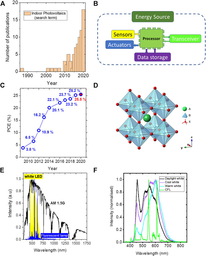
FIGURE 1. (A) The graph showing the number of IPV related publications as a function of year. (B) The main components in an IoT system. (C) The advancement of PCE for hybrid perovskite solar cells over the last decade. (D) Perovskite crystal structure with cubic symmetry. Organic or inorganic cations occupy position A (green) whereas metal cations and halogens occupy the B (bluish-grey) and X (red) positions, respectively. (E) Comparison of 1 Sun spectrum to indoor artificial light spectra. (F) Spectra of different types of white LEDs and CFL lamp used inside the buildings.
The concept of the IoT, initially coined by Kevin Ashton in 1999, has now projected to be a 1.6 trillion market in 2025 (Kramp et al., 2013). IoT is a smart network of connected physical objects with embedded sensors and actuators. IoT industry is projected to make an economic impact of $11 trillion by 2025 and as many as 75 billion connected IoT devices. Furthermore, it is noticeable that half of those components to be installed will be located inside buildings (Mathews et al., 2019). Wireless sensors are the most fundamental components in these smart devices (Figure 1B) (Davies, 2015). Sustainably, powering these sensors is a huge challenge. At present, these sensors are powered by batteries which limit the IoT potential by service interruptions due to battery replacement and eventually cause an environmental problem (due to battery disposal). These sensors only require µW-mW of power for their efficient functioning. Light energy is available in the ambient environment and can be accessed easily via photovoltaic devices without requesting additional devices or multiple energy transfer, thus becoming the most promising candidate to power IoT sensor system.
Different types of PV materials including III-IV, CIGS, organic, dye-sensitized, and perovskite are taken into consideration for efficient indoor light harvesting. Table 1 shows the main photovoltaic materials available and their bandgap. In contrast to conventional solar cell technologies such as silicon, the emerging PV technologies based on organic and halide perovskite semiconductors have tunable bandgap. In the history of photovoltaics, no other light harvesting material has ever triggered research attention and promising avenues to harness solar energy similar to organometal halide perovskites (Jena et al., 2019; Miyasaka et al., 2020; Mhaisalkar et al., 2020). Within a decade, the power conversion efficiency (PCE) of these perovskite solar cells has made an amazing advancement from 3.81% in 2009 to 25.5% today (Figure 1C). Represented by a general chemical formula of ABX3, this family of materials provide a framework to bind organic and inorganic component to a molecular composite, where A is an organic or inorganic cation, B is a divalent cation, such as Pb2+ and Sn2+, and X is halogen, I−, Br−, or Cl−. Organic cations, A, can be methylammonium (MA) CH3NH3+, ethylammonium (EA) C2H5NH3+, formamidinium (FA) HC(NH2)2+, and even inorganic Cs (Figure 1D). These materials possess exceptional optoelectronic properties needed for a photovoltaic material such as direct bandgap which is tunable (1.17–3.3 eV), high absorption (absorption length of 200–300 nm) in the visible range, low exciton binding energy ∼30 meV (comparable to RT thermal energy), high electron and hole bulk mobility (∼2000 cm2/(V.s) and ∼300 cm2/(V.s), respectively), large diffusion length (>1 μm), and ability to form high-quality crystals at relatively low processing temperatures (RT to 150°C) via vacuum or wet synthesis methods (Grätzel, 2014; Stoumpos and Kanatzidis, 2015; Green et al., 2015; Park, 2015).
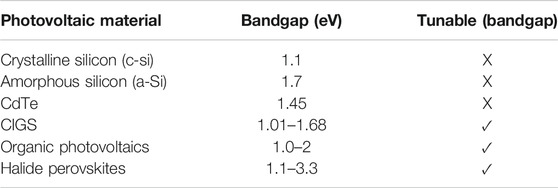
TABLE 1. Different photovoltaic materials and their bandgap.
The distributed nature of the IoT sensors requires that the indoor light energy harvesters also be distributed in nature. Thus, IPVs, which are suitable for powering the sensors, need to have high PCE, ease of processability, low cost, earth abundance of constituting materials, flexibility, conformability, and lightweight. Halide perovskite photovoltaic devices integrate all these requirements. Along with the extraordinary power conversion efficiency under one sun, halide perovskites have shown remarkable efficiency under indoor lighting as well. Even though recently Li et al. (2020), Chen (2019), and Lee et al. (2019b) have reviewed thin-film indoor photovoltaics, the growing potential and increasing number of publications related to halide perovskite IPVs demand a review focusing on the halide perovskite IPV itself.
Factors Affecting Indoor Light Harvesting
The common perception is that high-performance Si solar cells can perform the same under indoor lighting condition. This is not true and is especially pertinent with the phasing out of the incandescent light bulbs which have a similar broad emission spectrum to that of the solar spectrum. Identifying which photovoltaic technology is suitable for IPV depends mainly on the 1) indoor light spectrum and 2) factors determining the power conversion efficiency.
Indoor Light Spectrum and Maximum Theoretical Efficiency of IPVs
Indoor lighting in residential buildings and offices is now dominated by fluorescent lamps and white light-emitting diodes which are entirely different in intensity (1,000 times lower) and spectral content (narrow spectrum vs. broad) from the solar spectrum (Figure 1E). The intensity of standard sunlight spectrum (AM 1.5G) is 100 mW/cm2 and the typical indoor artificial light intensity is 0.05–1 mW/cm2 (∼200–2000 lux). The low available light intensity inside the building was one reason why indoor photovoltaic technology was not receiving much attention for many years. However, when the IoT gained popularity since 2010, indoor photovoltaics also started receiving its attention. This is because the IoT sensors only require µW-mW of power to operate. Depending on the correlated color temperature, three main types of white LED lighting used inside buildings are warm white, cool white, and daylight white. The typical spectra of these light sources are shown in (Figure 1F). As shown in the spectra, a warm white LED has a higher orange spectral range compared to blue; cool white LED has higher blue spectral content compared to warm white. Inside buildings, warm white LEDs are usually used in living rooms, bedrooms, and hallways. Cool white LEDs are usually used in kitchens, study areas, bathrooms, offices, and retail stores; daylight LEDs are used in commercial, retail, and art studios (integral-led.com).
Different spectral content and wavelength range of indoor light sources mean that the optimum bandgap and thermodynamically limited maximum power conversion efficiency (Shockley-Queisser limit) are different for indoor photovoltaics compared to outdoor solar cells. Under the solar spectrum (100 mW/cm2), the maximum theoretical efficiency is 33% and the optimum bandgap is 1.4 eV (Shockley and Queisser, 1961). In the case of indoor lighting conditions, the optimum material bandgap is ∼1.9 eV and the maximum theoretical efficiency can reach as high as ∼60% for LEDs and 50% for fluorescent lamps (Müller et al., 2013; Ho et al., 2020) (Figure 2A). This implies that the active layer composition of the perovskite indoor photovoltaics needs to be modified for higher photon energy indoor lightings compared to that of 1 Sun. This aspect is further detailed in Band Structure of Halide Perovskite Semiconductors.
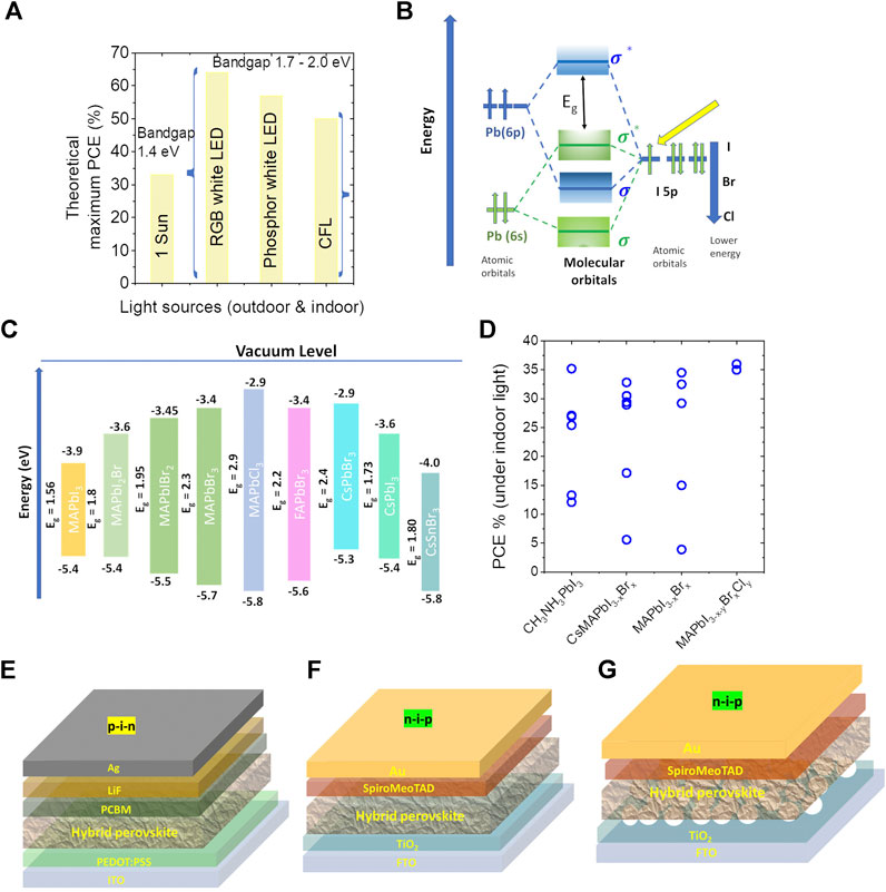
FIGURE 2. (A) Maximum theoretical efficiency of IPVs as a function of bandgap, (B) electronic band structure of halide perovskites, (C) some typical wide-bandgap halide perovskites, and (D) power conversion efficiency of halide perovskite indoor photovoltaic devices as a function of different composition. Different photovoltaic device architectures, (E) planar p-i-n, (F) planar n-i-p, and (G) mesoporous n-i-p architectures.
Indoor Photovoltaic Performance Parameters
The photovoltaic power conversion efficiency (ƞ) is determined by three performance parameters open-circuit voltage (Voc), short circuit current density (Jsc), and fill factor (FF) as
where
where I is the incident light intensity,
FF depends indirectly on the light intensity through the following relation (Green, 1981):
where
where
where
where
where
In this review, we will be mainly focusing on the wide-bandgap halide perovskite semiconductors suitable for indoor light harvesting. Halide perovskite bandgap can be tuned from 1.1 to 3.7 eV by interchanging/mixing B cation (Ge, Sn, and Pb) or halogens (X = Cl, Br and I) (Hu et al., 2019; Jena et al., 2019; Mhaisalkar et al., 2020). This is highly advantageous considering the different spectral features of the indoor light sources. Since the bandgap modification is required for maximizing indoor light harvesting, understanding the band structure of halide perovskite is highly important and constitutes the focus of discussion for the next section.
Band Structure of Halide Perovskite Semiconductors
Electronic band structure determines the optoelectronic properties such as optical absorption of the incoming photons, charge transfer from the active layer to the charge-transporting layers, and opportunity for bandgap engineering. Halide perovskites are direct bandgap semiconductors with sharp absorption edges. In halide perovskites, both the valence band maximum (VBM) and conduction band minimum (CBM) are constituted by antibonding sigma orbitals but with different degree of contribution from B cation and X anion
As the halide ions are moved from I (
With this background understanding of band structure of halide perovskites, in the next section, the indoor photovoltaic properties of halide perovskites would be reviewed with special emphasis on the selection of the active layer materials and the device architecture.
Halide Perovskite-Based Indoor Photovoltaics
Most of the initial reports on the indoor photovoltaic performance of hybrid perovskites were focused on the most widely investigated hybrid perovskite composition of CH3NH3PbI3. CH3NH3PbI3 has a bandgap of 1.56 eV, lower than the theoretically predicted optimum bandgap reported for indoor photovoltaics. By interface engineering and controlling the traps at the interfaces and carrier dynamics, CH3NH3PbI3-based indoor photovoltaic devices have demonstrated a power conversion efficiency ranging from 20% to 34% under indoor lighting conditions (Chen et al., 2015; Dagar et al., 2018; Lucarelli et al., 2017; Di Giacomo et al., 2016). Raifuku et al. (2016) have previously shown that hybrid perovskite solar cells perform better under low-intensity illumination such as 0.1 mW/cm2, compared to crystalline silicon. They demonstrated that, at low-intensity levels, perovskite solar cells can retain 70% of their open-circuit voltage at 1 Sun. Concerning interface engineering in indoor photovoltaics, the study reported by Li et al. is highly significant as they demonstrated that the ionic liquid of 1-butyl-3-methylimidazolium tetrafluoroborate ([BMIM]BF4) can passivate the surface traps on the electron transport layer of PCBM and prevent moisture and oxygen erosion to the perovskite active layer. These indoor photovoltaic devices based on CH3NH3PbI3 showed a power conversion efficiency of 35.2% under indoor lighting conditions (Li et al., 2018).
We have previously reported that, compared to CH3NH3PbI3, the mixed halides of iodide-bromide and iodide-chloride can have a higher power conversion efficiency of 23% under indoor white LED and CFL lighting (Jagadamma et al., 2019). In 2018, Guo et al. showed that CH3NH3PbI3 doped with Cl and citric acid can convert indoor white LED light to electricity with 26% power conversion efficiency. They attribute this enhanced efficiency to the perovskite crystal modulation effects and their improved quality (Guo et al., 2017). Very recently, Sun et al. reported bandgap engineered Cs0.05MA0.95PbBrxI3-x perovskites with a systematic variation of its bandgap from 1.6 to 1.75 eV by increasing the bromide to iodide ratio. These solar cells demonstrated a record efficiency of 36% under white light-emitting diode and 33.2% under CFL lamp (Sun et al., 2020). Using the similar approach of composition engineering to tune the bandgap of CH3NH3PbI3, that is by increasing the bromide to iodide ratio (1.56 eV–1.76 eV), very recently Lim et al. have also reported a power conversion efficiency of 34% under white LED illumination (Lim et al., 2020). Triple cation and triple anion-based perovskite solar cells have also been tested for their efficiency under indoor lighting conditions. Under white LED illumination, CsFAMA triple cation-based devices demonstrated a PCE of 21% (Mica et al., 2020). By adjusting the anion I/Br/Cl content in the MAPbI3−x-yBryClx composition, the bandgap was tuned from 1.6 to 1.8 eV and record indoor PCE of 36% was demonstrated (Cheng et al., 2019). It should be noted that, among the various perovskite-based IPVs reported so far, this bandgap-tuned composition of 1.8 eV has resulted in the highest Voc (>1 V) under 1,000 lux white LED indoor illumination. Pb-free perovskites are also gaining attention in indoor PV application and a very recent report showed a PCE of 4.5% under white LED illumination (Peng et al., 2020). In Figure 2D, the power conversion efficiency of halide perovskite indoor photovoltaics as a function of their composition is provided. Figure 2D shows that the CH3NH3PbI3 solar cells with interface engineering are giving a comparable performance to bandgap engineered wide-bandgap semiconductors. This implies that there is enough room to improve the PCE of wide-bandgap halide perovskites by interface engineering and modifying the device architecture. To understand the role of device architecture on the Voc loss (and hence on power conversion efficiency), indoor photovoltaic efficiency as a function of different architecture is reviewed in the next section.
This is partly motivated by the report by Raifuku et al., where they showed that, under low light intensity, planar, structure outperforms mesoporous architecture and retains better Voc under low-intensity illumination (Raifuku et al., 2016). The two common device architectures in perovskite solar cells are n-i-p and p-i-n as shown in Figures 2E and 2F. In n-i-p configuration, there is mesoporous and planar device configuration. Table 2 lists a summary of PCE (and Voc) of halide perovskite indoor photovoltaics as a function of device architecture. Both n-i-p and p-i-n PV device architectures are found to be showing good power conversion efficiencies under indoor lighting. Previously, Lee et al. have reported the significance of selecting different device architectures and the functional layers in maximizing the power output of indoor photovoltaics devices (Lee et al., 2019a). They have noticed that in mesoporous n-i-p architecture replacing the Spiro-MeOTAD hole transporting layer with PTAA reduces the output power dramatically and in inverted p-i-n architecture, replacing the PEDOT:PSS HTL by Poly-TPD enhances the maximum output power.
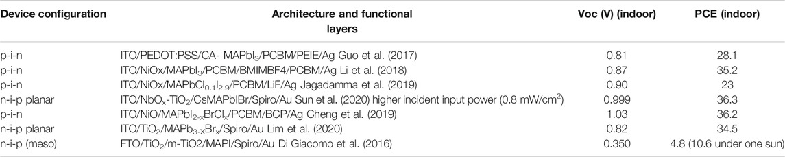
TABLE 2. PCE and Voc of some typical halide perovskite-based indoor photovoltaics with different functional layers and device architecture.
Challenges and Future Outlook
Halide perovskite semiconductors have thus already demonstrated their remarkable potential in realizing highly efficient IPVs. However, along with further efforts toward achieving the theoretically predicted PCE and accelerating their real-life application in IoT systems, the following challenges need to be addressed.
Photo-Induced Phase Segregation
Normally, wide-bandgap halide perovskites are obtained by replacing iodide (I-) ions with bromide (Br-), to form mixed halides. However, when the Br content is more than 20%, halide phase segregation (iodide rich and bromide rich phases) occurs upon photoexcitation of mixed halide perovskites (Hoke et al., 2015). The iodide-rich regions act as traps for photogenerated carriers and limit the open-circuit voltage in the corresponding solar cells. So, the advantage of the wide bandgap is not reflected in the open-circuit voltage of the IPV as expected (Yang et al., 2018). The voltage deficit can be expressed as
Stability and Pb Toxicity
Like outdoor perovskite solar cells, the indoor perovskite solar cells should also demonstrate high stability and robust encapsulation to prevent any Pb leakage to the indoor ambient. Compared to outdoor conditions, inside the buildings, these devices are exposed to mild weather conditions in terms of temperature and humidity. Even though extensive stability characterization standards are available for outdoor solar cells, no standard stability test conditions exist for indoor photovoltaics and a new stability standard has to be developed for indoor photovoltaics (Khenkin et al., 2020).
S-Shape Challenge
In indoor photovoltaic devices using metal oxide transport layers such as SnO2, TiO2, ZnO, there is a possibility that these devices suffer s-shape challenge (light soaking effect) limiting the power conversion efficiency (Jiang et al., 2018; Yan et al., 2017). These metal oxide layers have defects which are filled during the 1 Sun measurement due to the UV-spectral component and high incident light intensity. However, since indoor light has no UV-spectral component and low intensity, the s-shape challenge is more critical for indoor photovoltaics. More research efforts would need to develop metal oxide charge-transporting layers suitable for indoor applications and need no UV excitation to fill the trap states.
Voc Loss
Voltage loss of the indoor perovskite photovoltaic devices is much higher compared to the outdoor 1 Sun solar cell devices. Comparing the optimum bandgap differences (1.4 eV vs. 1.9 eV), presently, the Voc loss is more than 1 V for the indoor PVs even if the intensity differences are accounted. One main reason is that wide-bandgap perovskite solar cells usually suffer from high Voc losses with respect to their theoretical limit (Mahesh et al., 2020). There should be more research efforts to enhance the Voc improvement of indoor perovskite solar cells to achieve the theoretically predicted maximum power conversion efficiency of 50%–60%.
Author Contributions
LJ designed the manuscript and wrote the substantial part of the manuscript, and SW also contributed to writing. Both authors agree with the content of the work.
Funding
LJ acknowledges the funding through the UKRI-Future Leaders Fellowship (MR/T022094/1).
Conflict of Interest
The authors declare that the research was conducted in the absence of any commercial or financial relationships that could be construed as a potential conflict of interest.
Acknowledgments
LJ acknowledges Julia Payne, School of Chemistry, University of St Andrews, for providing the crystal structure of halide perovskites.
References
Chen, C.-Y., Chang, J.-H., Chiang, K.-M., Lin, H.-L., Hsiao, S.-Y., and Lin, H.-W. (2015). Perovskite photovoltaics for dim-light applications. Adv. Funct. Mater. 25, 7064–7070. doi:10.1002/adfm.201503448
Chen, F.-C. (2019). Emerging organic and organic/inorganic hybrid photovoltaic devices for specialty applications: low-level-lighting energy conversion and biomedical treatment. Adv. Opt. Mater. 7, 1800662. doi:10.1002/adom.201800662
Cheng, R., Chung, C. C., Zhang, H., Liu, F., Wang, W. T., Zhou, Z., et al. (2019). Tailoring triple-anion perovskite material for indoor light harvesting with restrained halide segregation and record high efficiency beyond 36%. Adv. Energy Mater. 9, 1901980. doi:10.1002/aenm.201901980
Dagar, J., Castro-Hermosa, S., Lucarelli, G., Cacialli, F., and Brown, T. M. (2018). Highly efficient perovskite solar cells for light harvesting under indoor illumination via solution processed SnO2/MgO composite electron transport layers. Nano Energy 49, 290–299. doi:10.1016/j.nanoen.2018.04.027
Davies, R. (2015). The internet of things opportunities and challenges. Available at: https://www.europarl.europa.eu/RegData/etudes/BRIE/2015/557012/EPRS_BRI(2015)557012_EN.pdf.
Di Giacomo, F., Zardetto, V., Lucarelli, G., Cinà, L., Di Carlo, A., Creatore, M., et al. (2016). Mesoporous perovskite solar cells and the role of nanoscale compact layers for remarkable all-round high efficiency under both indoor and outdoor illumination. Nano Energy 30, 460–469. doi:10.1016/j.nanoen.2016.10.030
Elumalai, N., Mahmud, M., Wang, D., and Uddin, A. (2016). Perovskite solar cells: progress and advancements. Energies 9, 861. doi:10.3390/en9110861
Goo, J. S., Shin, S.-C., You, Y.-J., and Shim, J. W. (2018). Polymer surface modification to optimize inverted organic photovoltaic devices under indoor light conditions. Solar Energ. Mater. Solar Cell 184, 31–37. doi:10.1016/j.solmat.2018.04.023
Grätzel, M. (2014). The light and shade of perovskite solar cells. Nat. Mater. 13, 838–842. doi:10.1038/nmat4065
Green, M. A., Jiang, Y., Soufiani, A. M., and Ho-Baillie, A. (2015). Optical properties of photovoltaic organic-inorganic lead halide perovskites. J. Phys. Chem. Lett. 6, 4774–4785. doi:10.1021/acs.jpclett.5b01865
Green, M. A. (1981). Solar cell fill factors: general graph and empirical expressions. Solid-State Electron. 24, 788–789. doi:10.1016/0038-1101(81)90062-9
Guo, Y., Sato, W., Shoyama, K., Halim, H., Itabashi, Y., Shang, R., et al. (2017). Citric Acid modulated growth of oriented lead perovskite crystals for efficient solar cells. J. Am. Chem. Soc. 139, 9598–9604. doi:10.1021/jacs.7b03856
He, X., Qiu, Y., and Yang, S. (2017). Fully-inorganic trihalide perovskite nanocrystals: a new research frontier of optoelectronic materials. Adv. Mater. 29, 1700775. doi:10.1002/adma.201700775
Ho, J. K. W., Yin, H., and So, S. K. (2020). From 33% to 57%-An elevated potential of efficiency limit for indoor photovoltaics. J. Mater. Chem. A 8, 1717–1723. doi:10.1039/c9ta11894b
Hoke, E. T., Slotcavage, D. J., Dohner, E. R., Bowring, A. R., Karunadasa, H. I., and McGehee, M. D. (2015). Reversible photo-induced trap formation in mixed-halide hybrid perovskites for photovoltaics. Chem. Sci. 6, 613–617. doi:10.1039/c4sc03141e
Hu, Z., Lin, Z., Su, J., Zhang, J., Chang, J., and Hao, Y. (2019). A review on energy band‐gap engineering for perovskite photovoltaics. Sol. RRL 3, 1900304–1900309. doi:10.1002/solr.201900304
Huang, H., Bodnarchuk, M. I., Kershaw, S. V., Kovalenko, M. V., and Rogach, A. L. (2017). Lead halide perovskite nanocrystals in the research spotlight: stability and defect tolerance. ACS Energy Lett. 2, 2071–2083. doi:10.1021/acsenergylett.7b00547
Huang, J., Xiang, S., Yu, J., and Li, C.-Z. (2019). Highly efficient prismatic perovskite solar cells. Energy Environ. Sci. 12, 929–937. doi:10.1039/c8ee02575d
integral-led.com. Available at: https://integral-led.com/education/warm-white-or-c.
Jagadamma, L. K., Blaszczyk, O., Sajjad, M. T., Ruseckas, A., and Samuel, I. D. W. (2019). Efficient indoor p-i-n hybrid perovskite solar cells using low temperature solution processed NiO as hole extraction layers. Solar Energ. Mater. Solar Cell 201, 110071. doi:10.1016/j.solmat.2019.110071
Jena, A. K., Kulkarni, A., and Miyasaka, T. (2019). Halide perovskite photovoltaics: background, status, and future prospects. Chem. Rev. 119, 3036–3103. doi:10.1021/acs.chemrev.8b00539
Jiang, Z., Soltanian, S., Gholamkhass, B., Aljaafari, A., and Servati, P. (2018). Light-soaking free organic photovoltaic devices with sol-gel deposited ZnO and AZO electron transport layers. RSC Adv. 8, 36542–36548. doi:10.1039/C8RA07071G
Kang, J., and Wang, L. W. (2017). High defect tolerance in lead halide perovskite CsPbBr3. J. Phys. Chem. Lett. 8, 489–493. doi:10.1021/acs.jpclett.6b02800
Khenkin, M. V., Katz, E. A., Abate, A., Bardizza, G., Berry, J. J., Brabec, C., et al. (2020). Consensus statement for stability assessment and reporting for perovskite photovoltaics based on ISOS procedures. Nat. Energ. 5, 35–49. doi:10.1038/s41560-019-0529-5
Koster, L. J. A., Mihailetchi, V. D., Ramaker, R., and Blom, P. W. M. (2005). Light intensity dependence of open-circuit voltage of polymer:fullerene solar cells. Appl. Phys. Lett. 86, 123509–123513. doi:10.1063/1.1889240
Kramp, T., van Kranenburg, R., and Lange, S. (2013). Introduction to the internet of things. Berlin, Germany: Springer.
Lee, H. K. H., Barbé, J., Meroni, S. M. P., Du, T., Lin, C.-T., Pockett, A., et al. (2019a). Outstanding indoor performance of perovskite photovoltaic cells - effect of device architectures and interlayers. Sol. RRL 3, 1800207. doi:10.1002/solr.201800207
Lee, H. K. H., Barbé, J., and Tsoi, W. C. (2019b). Organic and perovskite photovoltaics for indoor applications. Amsterdam, The Netherlands: Elsevier.
Li, M., Igbari, F., Wang, Z. K., and Liao, L. S. (2020). Indoor thin‐film photovoltaics: progress and challenges. Adv. Energ. Mater. 10, 2000641. doi:10.1002/aenm.202000641
Li, M., Zhao, C., Wang, Z. K., Zhang, C. C., Lee, H. K. H., Pockett, A., et al. (2018). Interface modification by ionic liquid: a promising candidate for indoor light harvesting and stability improvement of planar perovskite solar cells. Adv. Energ. Mater. 8, 1801509. doi:10.1002/aenm.201801509
Lim, J. W., Kwon, H., Kim, S. H., You, Y. J., Goo, J. S., Ko, D. H., et al. (2020). Unprecedentedly high indoor performance (efficiency > 34 %) of perovskite photovoltaics with controlled bromine doping. Nano Energy 75, 104984. doi:10.1016/j.nanoen.2020.104984
Lucarelli, G., Di Giacomo, F., Zardetto, V., Creatore, M., and Brown, T. M. (2017). Efficient light harvesting from flexible perovskite solar cells under indoor white light-emitting diode illumination. Nano Res. 10, 2130–2145. doi:10.1007/s12274-016-1402-5
Mahesh, S., Ball, J. M., Oliver, R. D. J., McMeekin, D. P., Nayak, P. K., Johnston, M. B., et al. (2020). Revealing the origin of voltage loss in mixed-halide perovskite solar cells. Energ. Environ. Sci. 13, 258–267. doi:10.1039/c9ee02162k
Mathews, I., Kantareddy, S. N., Buonassisi, T., and Peters, I. M. (2019). Technology and market perspective for indoor photovoltaic cells. Joule 3, 1415–1426. doi:10.1016/j.joule.2019.03.026
Mhaisalkar, S. G., Mathews, N., Bolink, H. J., and Bahulayan, D. (2020). Advances in perovskite optoelectronics: bridging the gap between laboratory and fabrication. Adv. Energ. Mater. 10, 2000393. doi:10.1002/aenm.202000393
Mica, N. A., Bian, R., Manousiadis, P., Jagadamma, L. K., Tavakkolnia, I., Haas, H., et al. (2020). Triple-cation perovskite solar cells for visible light communications. Photon. Res. 8, A16–A24. doi:10.1364/prj.393647
Minnaert, B., and Veelaert, P. (2014). A proposal for typical artificial light sources for the characterization of indoor photovoltaic applications. Energies 7, 1500–1516. doi:10.3390/en7031500
Miyasaka, T., Kulkarni, A., Kim, G. M., Öz, S., and Jena, A. K. (2020). Perovskite solar cells: can we go organic‐free, lead‐free, and dopant‐free? Adv. Energ. Mater. 10, 1902500. doi:10.1002/aenm.201902500
Müller, M. F., Freunek, M., and Reindl, L. M. (2013). Maximum efficiencies of indoor photovoltaic devices. IEEE J. Photovoltaics 3, 59–64. doi:10.1109/JPHOTOV.2012.2225023
Olthof, S. (2016). Research Update: the electronic structure of hybrid perovskite layers and their energetic alignment in devices. APL Mater. 4, 091502. doi:10.1063/1.4960112
Park, N.-G. (2015). Perovskite solar cells: an emerging photovoltaic technology. Mater. Today 18, 65–72. doi:10.1016/j.mattod.2014.07.007
Peng, Y., Huq, T. N., Mei, J., Portilla, L., Jagt, R. A., Occhipinti, L. G., et al. (2020). Lead‐free perovskite‐inspired absorbers for indoor photovoltaics. Adv. Energ. Mater. 11, 2002761. doi:10.1002/aenm.202002761
Raifuku, I., Ishikawa, Y., Ito, S., and Uraoka, Y. (2016). Characteristics of perovskite solar cells under low-illuminance conditions. J. Phys. Chem. C 120, 18986–18990. doi:10.1021/acs.jpcc.6b05298
Ravi, V. K., Markad, G. B., and Nag, A. (2016). Band edge energies and excitonic transition probabilities of colloidal CsPbX3 (X = Cl, Br, I) perovskite nanocrystals. ACS Energ. Lett. 1, 665–671. doi:10.1021/acsenergylett.6b00337
Shockley, W., and Queisser, H. J. (1961). Detailed balance limit of efficiency of p‐n junction solar cells. J. Appl. Phys. 32, 510–519. doi:10.1063/1.1736034
Steim, R., Ameri, T., Schilinsky, P., Waldauf, C., Dennler, G., Scharber, M., et al. (2011). Organic photovoltaics for low light applications. Solar Energ. Mater. Solar Cell 95, 3256–3261. doi:10.1016/j.solmat.2011.07.011
Stoumpos, C. C., and Kanatzidis, M. G. (2015). The renaissance of halide perovskites and their evolution as emerging semiconductors. Acc. Chem. Res. 48, 2791–2802. doi:10.1021/acs.accounts.5b00229
Sun, H., Deng, K., Jiang, Y., Ni, J., Xiong, J., and Li, L. (2020). Realizing stable Artificial photon energy harvesting based on perovskite solar cells for diverse applications. Small 16, 1906681. doi:10.1002/smll.201906681
Tao, S., Schmidt, I., Brocks, G., Jiang, J., Tranca, I., Meerholz, K., et al. (2019). Absolute energy level positions in tin- and lead-based halide perovskites. Nat. Commun. 10, 2560. doi:10.1038/s41467-019-10468-7
Tong, J., Jiang, Q., Zhang, F., Kang, S. B., Kim, D. H., and Zhu, K. (2020). Wide-bandgap metal halide perovskites for tandem solar cells. ACS Energ. Lett. 6, 232–248. doi:10.1021/acsenergylett.0c02105
Walsh, A. (2015). Principles of chemical bonding and band gap engineering in hybrid organic-inorganic halide perovskites. J. Phys. Chem. C 119, 5755–5760. doi:10.1021/jp512420b
Wu, Y., Chen, W., Chen, G., Liu, L., He, Z., and Liu, R. (2018). The impact of hybrid compositional film/structure on organic-inorganic perovskite solar cells. Nanomaterials 8, 356–427. doi:10.3390/nano8060356
Yan, Y., Cai, F., Yang, L., Li, J., Zhang, Y., Qin, F., et al. (2017). Light-soaking-free inverted polymer solar cells with an efficiency of 10.5% by compositional and surface modifications to a low-temperature-processed TiO2electron-transport layer. Adv. Mater. 29. doi:10.1002/adma.201604044
Keywords: composition tuning, triple cation, triple anion, CH3NH3PbI3, internet of things, power conversion efficiency, indoor light spectra
Citation: Jagadamma LK and Wang S (2021) Wide-Bandgap Halide Perovskites for Indoor Photovoltaics. Front. Chem. 9:632021. doi: 10.3389/fchem.2021.632021
Received: 23 November 2020; Accepted: 27 January 2021;
Published: 26 March 2021.
Edited by:
Ping Yu, Institute of Chemistry (CAS), ChinaReviewed by:
Dillip K. Panda, Clemson University, United StatesFang Hao, General Motors (United States), United States
Copyright © 2021 Jagadamma and Wang. This is an open-access article distributed under the terms of the Creative Commons Attribution License (CC BY). The use, distribution or reproduction in other forums is permitted, provided the original author(s) and the copyright owner(s) are credited and that the original publication in this journal is cited, in accordance with accepted academic practice. No use, distribution or reproduction is permitted which does not comply with these terms.
*Correspondence: Lethy Krishnan Jagadamma, lkj2@st-andrews.ac.uk