Development and characterisation of caesium lead halide perovskite nanocomposite scintillators for X-ray detection
 Joseph O’Neill1*
  Isabel Braddock1
  Carol Crean2
  Joydip Ghosh1
  Mateus Masteghin3
  Sion Richards4 Matthew Wilson4
  Paul Sellin1
- 1Department of Physics, University of Surrey, Guildford, United Kingdom
- 2Department of Chemistry, University of Surrey, Guildford, United Kingdom
- 3Advanced Technology Institute, University of Surrey, Guildford, United Kingdom
- 4Science and Technology Facilities Council, Rutherford Appleton Laboratory, Harwell Campus, Didcot, United Kingdom
We present work on the development of mixed-halide perovskite (CsPbClxBr(1−x)) nanocrystal scintillators for X-ray detection applications. The effect of the varying the halide composition on the resulting peak emission and light yield is discussed, with the CsPbBr3 materials displaying the greatest light yield. These perovskite nanocrystals were successfully loaded into PMMA, an inert plastic, at 2% mass weighting and the responses of these composites were compared to that of their colloidal dispersions. The composites were also characterised in terms of the radioluminescent light yield and decay response, alongside their X-ray sensitivity, in which the PMMA-CsPbBr3 composites again outperformed the materials containing Cl− anions.
1 Introduction
Lead halide perovskites are a class of material following the structure of the ABX3 perovskite, where the B-cation site is occupied by Pb2+ and the X-anion site is a range of halides, e.g., Cl−, Br− and I− [1]. Pb2+ is an ideal component for these materials as radiation detectors, as its high-Z number ensures a large X-ray cross section and quantum efficiency. A benefit of the material is the tunable peak emission wavelength that the ratio of the anion site halide can bring. By varying the relative amounts of Cl, Br and I the peak emission from lead halide perovskites can be varied from 400–700 nm [2,3] by altering the semiconductor’s band gap. By matching the spectrum emission of the perovskite to an associated photosensor, the system can be optimised to increase the overall efficiency of the detector. Additionally, the change in halide has effects on the scintillation decay time of the material as the band gap increases [4, 5], allowing further customisation for the system.
Previous work has shown that the A site cation can be widely varied, affecting the stability and electrical conductivity of the perovskite [6]. Choices include organic compounds, such as
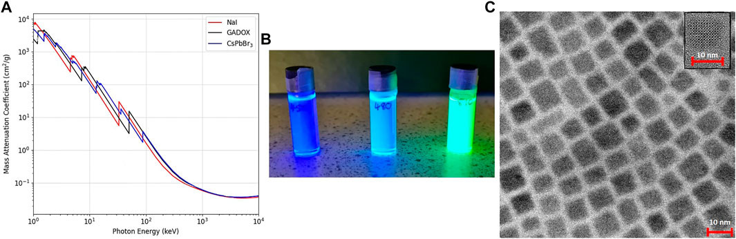
FIGURE 1. (A) Mass attenuation coefficient plots for CsPbBr3, NaI and GADOX. (B) Dispersions of CsPbX3 in toluene scintillating under UV light. (C) TEM images of CsPbBr3 NCs.
Perovskites can be used as both semiconductors and scintillators. For semiconductor purposes, perovskites are typically synthesised via melt-growth methods, such as the Bridgman method or solution growth methods. The Bridgman method can grow centimetre scale single crystals to be used for single crystal gamma spectroscopy [7]. Large polycrystalline materials can be formed via solution growth and then milled and pressed into wafers, for use as X-ray imaging systems [11] and dosimeters. Perovskites can also be used as scintillation radiation detectors, either in bulk form or as nanocomposites. This work covers characterisation of nanocomposite scintillators containing perovskite nanoparticles.
Perovskite nanoparticles have a light yield comparable or exceeding that of industry standard scintillators, benefiting both from the high X-ray sensitivity of the perovskite and also the increased light yield resulting from quantum confinement effects in the nanoparticles. Due to their structure, X-ray excitation leads to an excited triplet state, which has a high emission and fast decay time [12]. This likely originates from the strong spin–orbit coupling in the conduction band of the perovskite [13, 14], which allows for a fast single photon emission. However, perovskite nanoparticles do have limitations. The self-absorption of emitted light is an issue due to the low Stokes-shift of the system or from Mie scattering of the nanoparticles themselves [15]. This can be alleviated by adjusting the cations in the perovskite structure, using energy transfer processes such as FRET to shift the emitted light outside the absorption range of the material, and by adjusting the perovskite structure to increase the photon recycling efficiency [16].
The transparency of the composite must also be optimised, balancing a sufficiently high mass loading of nanoparticles to ensure a high quantum efficiency with the impact of the mass loading on the internal scattering arising from the nanoparticles. This can be resolved by ensuring an even distribution of nanoparticles in the composites during synthesis, and by limiting the material thickness to a few millimetres. Finally, perovskite nanoparticles are limited by their environmental stability. Lead halide perovskites are extremely hygroscopic and often have a short shelf life without the addition of stabilising agents such as ligands. By loading the nanoparticles into PMMA they are protected from the ambient environment and show a good level of stability.
Perovskite nanocrystals can be synthesised via a range of methods, including solid-state mechanosynthesis [17], precipitation [18] and hot injection [14]. These can produce materials in the size range of 5–100 nm, the size range in which quantum confinement effects can occur. CsPbX3 nanoparticles have been recently shown to act as a scintillator, with a light yield reported to be 17,000 photons per MeV [19]. Composite perovskite scintillators are an active area of research, with recent work on FAPbX3-PMMA composite scintillators reported as a viable direct X-ray imaging device [4]. In this work we report the production and analysis of 1 mm thick nanocomposite materials loaded with commercially available CsPbX3 nanoparticles, with a high X-ray stopping power and transmission. A range of blue-green emitting nanoparticles were purchased, characterised and loaded into PMMA disks and their optical properties characterised, including their peak emission wavelength and time response to both laser and X-ray excitation.
2 Methods
2.1 Materials and composite fabrication
Dispersions of three different CsPbX3 nanocrystals were purchased from the supplier Quantum Solutions. The three different compositions have peak emission wavelengths of 450, 480 and 510 nm, and the nanoparticles have a nominal diameter of ∼10 nm. The dispersions consisted of the CsPbX3, where X = Cl or Br, nanocrystals treated with oleic acid and oleylamine, dispersed in toluene (10 mg/mL) [20].
The PMMA composites were fabricated by mixing 1.5 g of PMMA (Aldrich) with a dispersion containing 30 mg of the dispersed nanocrystals in a vial with 3 mL of toluene. In preparation for the casting of the nanocrystals into the plastic, approximately 70% of the toluene was allowed to evaporate in a nitrogen-atmosphere glove box to increase the concentration of the dispersion to 17 mg/mL. The mixture was then heated at 56°C for 1 h on a hot plate, and stirred using a magnetic stirrer. The resulting mixture was then sonicated for 30 min to remove bubbles from the mixture and poured into 2 mm deep, 38 mm diameter moulds and left to cast over 2 days, covered to allow the toluene to recirculate and prevent the surface from distorting. The resulting composite disks were then removed from the moulds.
2.2 Characterisation methods
Transmission electron microscopy (TEM) imaging was performed with a Talos F200i TEM (Thermo Fisher Scientific). Dynamic light scattering (DLS) measurements were taken using a Zetasizer Nano S (Malvern Instruments), with the dispersion contained in square glass cuvettes. Photoluminescence (PL) spectra were taken with a 405 nm laser, recorded using a QE 6500 spectrometer (Ocean Insight), with a 420 nm long pass filter covering the collecting lens. For low temperature measurements, dropcast samples of the dispersions were mounted to a cryostat stage connected to a heating plate and liquid nitrogen supply, with the temperature set using a Temperature Measurement Control Unit TIC 304-MA (CryoVac). Absorption spectra were obtained using a UV-2401PC Spectrophotometer (Shimadzu). Time-resolved PL (TRPL) decay spectra were measured using a PicoQuant fluorescence lifetime spectrometer (PicoQuant), illuminated by a 405 nm laser pulsed with a DDS Function Generator (Aim-TTi). A 420 nm long pass filter covered the collecting lens. Scanning electron microscopy (SEM) imaging and energy dispersive X-ray spectroscopy (EDX) measurements were taken with a Thermo Scientific Apreo 2 SEM (Thermo Fisher Scientific).
Radioluminescence (RL) measurements were obtained with a QE 6500 spectrometer (Ocean Insight), connected to an integrating sphere (Labsphere) to ensure consistency of measurement geometry. The samples were irradiated by an X-ray tube (Hamamatsu) set to 80 kV and 100 μA. Time-resolved radioluminescence measurements were taken with samples coupled to a 8 mm diameter PMT (Hamamatsu H11901), housed within a copper Faraday cage. The samples were irradiated by a four-capacitor Scandiflash X-ray tube, with X-ray bursts 4 μs apart. The tube voltage was set to 75 kVp, and the current had a 2 kA maximum. X-ray sensitivity data was taken in a dark box, with the samples mounted to a 90° mirror stand, with the light collected with a 2 inch PMT (ET Enterprises). The X-ray source was a Mini-X X-ray tube, with the voltage set to 40 kV and the dose varied by adjusting the current between 10–200 μA in 10 μA steps.
3 Characterisation
3.1 Perovskite nanocrystal dispersions
The dispersions were reported to emit at 450, 480 and 510 nm, and to have a size of ∼10 nm by the manufacturer. The dispersions consisted of the CsPbX3 nanocrystals, where X = Cl or Br, treated with oleic acid and oleylamine, dispersed in toluene. A photo of the three different CsPbX3 nanocrystal dispersions scintillating under UV illumination can be seen in Figure 1B. TEM images of CsPbBr3 nanocrystals are shown in Figure 1C. The TEM imaging shows a well-ordered cubic morphology of the nanoparticles, and a size distribution of approximately 10 nm.
Once the materials had been received, the chemical compositions of the three nanoparticle dispersion were determined via EDX measurements taken with a SEM, utilising a circular backscatter (CBS) detector. The measured ratios of chlorine to bromine were found to be 1:1, 1:2 and 0:3 for the 450, 480 and 510 nm dispersions respectively. Therefore, it was determined that their structures were CsPbCl1.5Br1.5, CsPbClBr2 and CsPbBr3. The EDX spectra for samples of all three materials can be seen in Figure 2A, with the relevant peaks labelled, and the atomic percentages of the elements in Table 1. Si and Au peaks are labelled due to their presence in the measurement, with the samples placed on a silicon wafer and covered in a 3 nm gold layer.
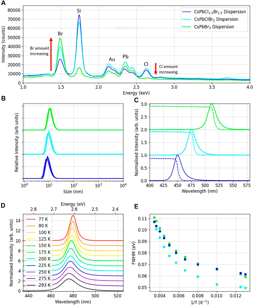
FIGURE 2. (A) EDX spectra of samples of the three CsPbClxBr1−x materials. (B) Size distributions of the dispersions measured using DLS. (C) Absorption and PL spectra of the dispersions. (D) PL emissions for the CsPbClBr2 dispersion over the temperature range 293-77K. (E) The FWHM against inverse temperature for the dispersions over the temperature range 293-77K.
TABLE 1. Atomic percentages of Cs, Pb, Cl and Br for the three CsPbX3 samples, measured with EDX.
Dynamic light scattering (DLS) measurements were performed to determine the size of the nanoparticles. Average sizes were 8 ± 1 nm for CsPbCl1.5Br1.5, 9 ± 1 nm for CsPbClBr2 and 10 ± 1 nm for CsPbBr3, consistent with the TEM imaging. The DLS spectra can be seen in Figure 2B, showing the relevant size distributions. As the bromine ratio increases, so too does the average particle size. For nanoparticles, as the size of the material decreases, the bandgap increases as the crystal lattice becomes smaller [21] and quantum confinement effects occur [22]. However, in these samples the halide present has a far greater impact on the bandgap, and therefore the emission peak of the samples is dominated by the amount of Br present, as can be seen in the photoluminescence spectra.
Normalised photoluminescence spectra of the nanocrystal dispersions can be seen in Figure 2C, illuminated by a 405 nm laser. The peak emission wavelengths for the dispersions were CsPbCl1.5Br1.5 = 450 ± 2 nm, CsPbClBr2 = 475 ± 2 nm and CsPbBr3 = 512 ± 2 nm, agreeing with the reported emission peak wavelengths from the supplier. CsPbBr3 NC thin films have been reported to have peak photoluminescence emissions of 508 nm for a thin film of 2 nm nanoparticles [23] and 550 nm for a thin film of 9 nm radii nanoparticles [19]. The range of peak emission wavelengths measured for these materials shows the impact of the size of the nanoparticles. In our samples the peak intensities of the dispersions increased with the amount of Br present. Taking the CsPbCl1.5Br1.5 peak intensity as 100%, the CsPbClBr2 had an intensity of 175% and the CsPbBr3 200% as shown in Supplementary Figure S1A The decreased light yield for lead halide perovskites with chlorine present has also been seen in studies of organic FA lead halide nanoparticles [4].
Absorption spectra are also shown in Figure 2C, with absorption edges at CsPbCl1.5Br1.5 = 446.0 ± .5 nm, CsPbClBr2 = 474.5 ± .5 nm and CsPbBr3 = 510.5 ± .5 nm. It can be determined that the resulting Stokes-shift of the dispersions is slight, on the order of 1 nm, indicating that self-absorption may be occurring at the higher energies of the emission.
To investigate the effect of temperature on the emission spectra, photoluminescence spectra were taken in the range 293–77 K with drop cast samples of all three dispersions. The various spectra for the CsPbCl1Br2 drop cast spectra can be seen in Figure 2D. It can be seen that as the temperature decreases, the intensity of the peak increases and the peak wavelength shifts to a lower energy. Upon cooling the bandgap decreases in these materials, unlike for traditional semiconductors, causing the red shift in the peak emission. Due to the low exciton binding energy, there is also a significant increase in light intensity upon cooling. Figure 2E shows that for all three dispersions the FWHM of the spectra decreases with temperature, due to a reduction in thermal broadening [24]. Sub-structure in the photoluminescence spectra due to exciton emission is not observed in our data acquired at 77K, which would require temperatures of around 10K to be visible [25, 26].
3.2 Nanocomposite disks
To investigate the response of the nanoparticles in a solid matrix, and to obtain reliable radiation measurements that are difficult to perform with dispersions, plastic nanocomposite disks were produced. The plastic used was the optically-inactive and chemically inert PMMA, and the nanoparticles were loaded at 2% weight. This amount was chosen to balance the requirement for a high mass attenuation coefficient for photoelectric absorption with the need to minimise incoherent scattering, which would otherwise have a detrimental effect on the optical transmission of the nanocomposite materials. A photo of typical 1 mm thick, 38 mm diameter disks can be seen in Figure 3A. Figure 3B shows a scanning electron microscope image taken using the circular back scatter detector at 1,500× zoom of a PMMA disk loaded with CsPbBr3 nanocrystals. The image is of a cross section of the composite disk. The nanocrystals appear as the bright spots in the image due to their high-Z compared to the plastic matrix and are evenly distributed throughout the sample. The cross section can be seen to contain many small voids. The loaded composites contain microbubbles resulting from the evaporation of the toluene introduced with the dispersion during the casting process. As discussed in the methods section, the plastic mixtures are treated via sonication and vacuum cycling to reduce the size of these bubbles, to diminish their impact on the transmission of the sample.
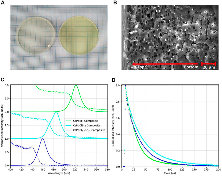
FIGURE 3. (A) 3.8 cm diameter plastic disks loaded with CsPbX3 nanocrystals. (B) A 1,500× zoom SEM image of a cross section of a PMMA disk loaded with a mixed halide dispersion. The white particles in the image are the perovskite nanocrystals spread across the thickness of the disk. (C) Absorption and emission spectra for the composite disks. (D) Time decay profiles of the disks under illumination by a 405 nm laser pulsed at 2.5 MHz.
Normalised photoluminescence spectra of the composite disks are shown in Figure 3C. The PMMA composites have peak emission wavelengths of CsPbCl1.5Br1.5 = 457 ± 2 nm, CsPbClBr2 = 482 ± 2 nm and CsPbBr3 = 517 ± 2 nm. All three composite disks have a peak wavelength emission that is ∼ 6 nm higher than their respective dispersions, indicating the some degree of nanoparticle agglomeration has occurred in the PMMA. Non-normalised spectra are shown in Supplementary Figure S1B. Absorption spectra are also shown in Figure 3C, with absorption edges at CsPbCl1.5Br1.5 = 439.0 ± .5 nm, CsPbClBr2 = 464.3 ± .5 nm and CsPbBr3 = 505.7 ± .5 nm. These have also been shifted compared with the nanocrystal dispersions, with the absorption edge for all the composite disks at a lower wavelength. This results in larger Stokes shifts for all three composites: CsPbCl1.5Br1.5 = 18 ± 2 nm, CsPbClBr2 = 17 ± 2 nm and CsPbBr3 = 11 ± 2 nm. This increase in the Stokes shifts of the nanoparticles in PMMA, compared to the dispersions, will tend to reduce the degree of self-absorption of the scintillation light in the plastic disks. The disks were illuminated by a 405 nm laser pulsed at 2.5 MHz to obtain photoluminescence decay spectra. The decay spectra are shown in Figure 3D, and were fitted with a biexponential fit, from which the average decay times were extracted. All the samples had a short decay time component of 9 ns. The long component of the decay of the PMMA composites were determined to be: CsPbCl1.5Br1.5 = 26.7 ± .2 ns; CsPbClBr2 = 32.2 ± .3 ns and CsPbBr3 = 28.2 ± .4 ns, and the average decay times were: CsPbCl1.5Br1.5 = 11.4 ± .1 ns; CsPbClBr2 = 12.2 ± .1 ns and CsPbBr3 = 9.3 ± .1 ns. These values and their relative weightings can be seen in Table 2. Previous reports of decay times from CsPbBr3 nanocrystal materials have not observed this weak slow time component, with values of the slow component of 2.9 ns for a thin film of 9 nm nanocrystals [19] and 7.8 ns for a drop cast film of 15 nm nanocrystals [8], while CsPbCl3 have been reported to have slow component decay times of 5.4 ns for a drop cast film of 12 nm [8].
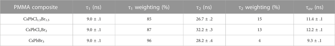
TABLE 2. Decay times and their relative weightings for the time decay curves of the CsPbX3 composites in PMMA, illuminated by a pulsed 405 nm laser and fit with biexponential curves.
X-ray measurements were carried out to characterise the X-ray response of the nanocomposite scintillators. Radioluminescence spectra of the composite disks were taken under illumination with an 80 kV 100 μA X-ray source, utilising an integrating sphere, the spectra are shown in Figure 4A. The PMMA composites have peak emissions of CsPbCl1.5Br1.5 = 458 ± 2 nm, CsPbClBr2 = 482 ± 2 nm and CsPbBr3 = 520 ± 2 nm. These values match their peak emissions from photoluminescence emission, showing that the radioluminescent optical emission due to X-rays is consistent with that observed for photoluminescence. CsPbBr3 nanocrystal thin films have been reported to have peak radioluminescence emissions at 532 nm under X-ray illumination at a dose rate of 278 μGy s−1 at 50 kV for a thin film of 9.6 nm nanocrystals [27]. The PMMA disk loaded with the CsPbCl1.5Br1.5 dispersion was considerably dimmer than the CsPbClBr2 and CsPbBr3 composites, as with the PL emissions from both the original dispersions and the composites. Taking the CsPbCl1.5Br1.5 integrated intensity as 100%, the CsPbClBr2 had an integrated intensity of 340% and the CsPbBr3 415%, as shown in Supplementary Figure S2A. This again shows the trend of increased light yield with increasing percentage of Br present in the perovskite nanocrystals.
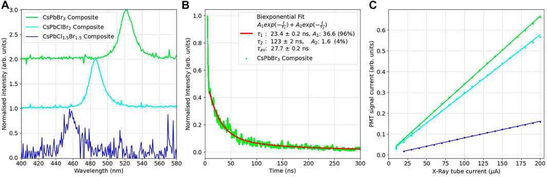
FIGURE 4. (A) Normalised RL spectra for the PMMA-mixed halide composite disks, illuminated by an 80 kV, 100 μA X-ray source. (B) Averaged time decay profiles of the PMMA-CsPbBr3 composite disk under illumination by a 75 kV, 2 kA X-ray source, pulsing for 35 ns. (C) RL intensity of the PMMA-mixed halide composite disks, as measured by a PMT at varying dose rates. The PMT signal current as has been adjusted for the quantum efficiency of the detector.
To compare to the decay times from time-resolved photoluminescence emission, time resolved radioluminescence was performed using a pulsed X-ray set. This X-ray set has a pulse width of approximately 35 ns, so any decay mechanisms faster than this time would be unavailable to resolve, however this setup would allow any slower decay components to be investigated. The averaged decay curves for the CsPbBr3 composite disk is shown in Figure 4B. The remaining spectra can be found in Supplementary Figure S3. In these spectra it can be seen that a short, ∼30 ns day is observed consistent with the pulse width of the X-ray source, along with a longer component at a lower intensity. The long decay times were determined to be CsPbCl1.5Br1.5 = 191 ± 6 ns, CsPbClBr2 = 206 ± 6 ns and CsPbBr3 = 123 ± 3 ns. These values and their relative weightings can be seen in Table 3. Previous work on drop cast films of CsPbBr3 nanocrystals has not observed this weaker, long-lived component when exposed to gamma sources, with a decay time of 44.6 ns reported under exposure to a pulsed 137Cs source [2].
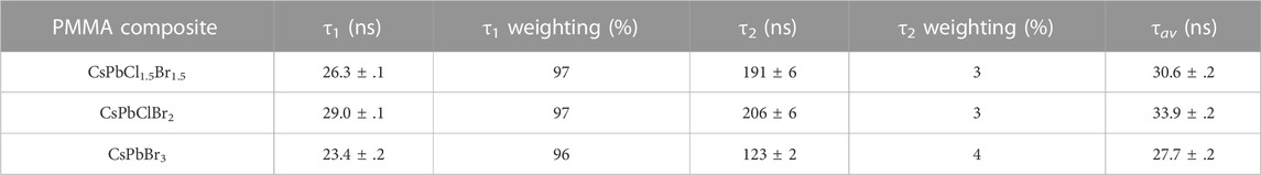
TABLE 3. Decay times and their relative weightings for the time decay curves of the CsPbX3 composites in PMMA, illuminated by a pulsed 100 kV 2 kA X-ray and fit with a biexponential curve.
The light response of the composite disks at different X-ray doses was measured with an X-ray tube, set at 40 kV and the current varied from 200 to 20 μA. The response data can be seen in Figure 4C. Consistent with the radioluminescence measurement, the PMMA composite disk loaded with the CsPbCl1.5Br1.5 nanocrystal dispersion was considerably dimmer than the CsPbClBr2 and CsPbBr3 composites. It can be seen that the composite disks have linear responses to X-ray radiation in this energy range, an important feature for X-ray detectors. The gradient of this response can be used to determine the sensitivity of the scintillators. Taking the CsPbCl1.5Br1.5 sensitivity as 100%, the CsPbClBr2 had an sensitivity of 350% and the CsPbBr3 413%. These relative values are similar to that of the relative radioluminescence integrated areas, showing that the relative light yields of the composites are independent of the photosensor used to measure the scintillated light.
4 Conclusion
In summary, the optical properties of commercial CsPbX3 nanoparticles were investigated, and their response to X-ray irradiation was studied. The nanocrystals were loaded into 1 mm thick PMMA disks to function as X-ray detectors, with the aim of producing a material that displayed the high radioluminescent light yield of perovskite nanocrystals whilst ensuring an even distribution of nanoparticles within the composites.
The nanocomposite materials present analogous peak wavelength emissions to their colloidal dispersions, and measurements showing the decay times of both laser and X-ray stimulated emission display consistent decay characteristics. The presence of chlorine in the perovskites can be seen to be linked to a decreased X-ray sensitivity and emission intensity, with the samples containing a higher ratio of bromine exhibiting superior performance.
Going forward, it is therefore recommended that the CsPbBr3 nanoparticles are utilised when creating nanocomposites for X-ray detectors. These are ideal for use as beamline detectors and are being developed as direct X-ray imaging systems.
Data availability statement
The raw data supporting the conclusion of this article will be made available by the authors, without undue reservation.
Author contributions
CC, MW, PS, and SR contributed to the conceptualisation of the study. The composites were fabricated by JO and IB. The characterisation was performed by JO, with assistance from IB, JG, MM, and SR. Analysis was performed by JO, with assistance from IB, CC, JG, and PS. All authors commented on the manuscript and aided in the reviewing process.
Funding
This research was carried out in collaboration with the Defense Threat Reduction Agency (DTRA), Interaction of Ionizing Radiation with Matter University Research Alliance (IIRM-URA), and was also supported under DTRA contract HDTRA1-18-1-0019. The project or effort depicted was or is sponsored by the Department of the Defense, Defense Threat Reduction Agency. The content of the information does not necessarily reflect the position or the policy of the federal government, and no official endorsement should be inferred. This work was also supported by the United Kingdom Engineering and Physical Research Council (Grant number EP/V036327/1). Author JO acknowledges studentship funding from STFC Rutherford Appleton Laboratory and the University of Surrey.
Acknowledgments
We would like to thank John-William Brown, Sarah Heisig, Michelle Williams, Rachida Bance-Soualhi and David Jones for technical support and training.
Conflict of interest
The authors declare that the research was conducted in the absence of any commercial or financial relationships that could be construed as a potential conflict of interest.
Publisher’s note
All claims expressed in this article are solely those of the authors and do not necessarily represent those of their affiliated organizations, or those of the publisher, the editors and the reviewers. Any product that may be evaluated in this article, or claim that may be made by its manufacturer, is not guaranteed or endorsed by the publisher.
Supplementary material
The Supplementary Material for this article can be found online at: https://www.frontiersin.org/articles/10.3389/fphy.2022.1046589/full#supplementary-material
References
1. Birowosuto M, Cortecchia D, Drozdowski W, Brylew K, Lachmanski W, Bruno A, et al. X-ray scintillation in lead halide perovskite crystals. Scientific Rep (2016) 6:37254–10. doi:10.1038/srep37254
2. Chen Q, Wu J, Ou X, Huang B, Almutlaq J, Zhumekenov AA, et al. All-inorganic perovskite nanocrystal scintillators. Nature (2018) 561:88–93. doi:10.1038/s41586-018-0451-1
3. Protesescu L, Yakunin S, Bodnarchuk MI, Krieg F, Caputo R, Hendon CH, et al. Nanocrystals of cesium lead halide perovskites (cspbx3, x= cl, br, and i): Novel optoelectronic materials showing bright emission with wide color gamut. Nano Lett (2015) 15:3692–6. doi:10.1021/nl5048779
4. Braddock IH, Al Sid Cheikh M, Ghosh J, Mulholland RE, O’Neill JG, Stolojan V, et al. Formamidinium lead halide perovskite nanocomposite scintillators. Nanomaterials (2022) 12:2141. doi:10.3390/nano12132141
5. Levchuk I, Osvet A, Tang X, Brandl M, Perea JD, Hoegl F, et al. Brightly luminescent and color-tunable formamidinium lead halide perovskite FAPbX3 (X = Cl, Br, I) colloidal nanocrystals. Nano Lett (2017) 17:2765–70. doi:10.1021/acs.nanolett.6b04781
6. Song J, Li J, Li X, Xu L, Dong Y, Zeng H. Quantum dot light-emitting diodes based on inorganic perovskite cesium lead halides (cspbx3). Adv Mater (2015) 27:7162–7. doi:10.1002/adma.201502567
7. Fu Y, Meng F, Rowley MB, Thompson BJ, Shearer MJ, Ma D, et al. Solution growth of single crystal methylammonium lead halide perovskite nanostructures for optoelectronic and photovoltaic applications. J Am Chem Soc (2015) 137:5810–8. doi:10.1021/jacs.5b02651
8. Dutta A, Behera RK, Pal P, Baitalik S, Pradhan N. Near-unity photoluminescence quantum efficiency for all cspbx3 (x= cl, br, and i) perovskite nanocrystals: A generic synthesis approach. Angew Chem Int Edition (2019) 58:5608–12. doi:10.1002/ange.201900374
9. Li Y, Zhou Z, Sheong FK, Xing Z, Lortz R, Wong KS, et al. Tuning the self-trapped emission: Reversible transformation to 0d copper clusters permits bright red emission in potassium and rubidium copper bromides. ACS Energ Lett (2021) 6:4383–9. doi:10.1021/acsenergylett.1c01957
10. Yang B, Yin L, Niu G, Yuan JH, Xue KH, Tan Z, et al. Lead-free halide rb2cubr3 as sensitive x-ray scintillator. Adv Mater (2019) 31:1904711. doi:10.1002/adma.201904711
11. Zhu W, Ma W, Su Y, Chen Z, Chen X, Ma Y, et al. Low-dose real-time x-ray imaging with nontoxic double perovskite scintillators. Light: Sci Appl (2020) 9:112–0. doi:10.1038/s41377-020-00353-0
12. Zhou F, Li Z, Lan W, Wang Q, Ding L, Jin Z. Halide perovskite, a potential scintillator for x-ray detection. Small Methods (2020) 4:2000506. doi:10.1002/smtd.202000506
13. Becker MA, Vaxenburg R, Nedelcu G, Sercel PC, Shabaev A, Mehl MJ, et al. Bright triplet excitons in caesium lead halide perovskites. Nature (2018) 553:189–93. doi:10.1038/nature25147
14. Zhou F, Li Z, Chen H, Wang Q, Ding L, Jin Z. Application of perovskite nanocrystals (ncs)/quantum dots (qds) in solar cells. Nano Energy (2020) 73:104757. doi:10.1016/j.nanoen.2020.104757
15. Xue J, Gu Y, Shan Q, Zou Y, Song J, Xu L, et al. Constructing mie-scattering porous interface-fused perovskite films to synergistically boost light harvesting and carrier transport. Angew Chem Int Edition (2017) 56:5316–20. doi:10.1002/ange.201700600
16. Fang Y, Wei H, Dong Q, Huang J. Quantification of re-absorption and re-emission processes to determine photon recycling efficiency in perovskite single crystals. Nat Commun (2017) 8:14417–9. doi:10.1038/ncomms14417
17. Ghosh J, Mawlong LP, Manasa G, Pattison AJ, Theis W, Chakraborty S, et al. Solid-state synthesis of stable and color tunable cesium lead halide perovskite nanocrystals and the mechanism of high-performance photodetection in a monolayer mos 2/cspbbr 3 vertical heterojunction. J Mater Chem C (2020) 8:8917–34. doi:10.1039/d0tc01306d
18. Dey A, Ye J, De A, Debroye E, Ha SK, Bladt E, et al. State of the art and prospects for halide perovskite nanocrystals. ACS nano (2021) 15:10775–981. doi:10.1021/acsnano.0c08903
19. Heo JH, Shin DH, Park JK, Kim DH, Lee SJ, Im SH. High-performance next-generation perovskite nanocrystal scintillator for nondestructive x-ray imaging. Adv Mater (2018) 30:1801743. doi:10.1002/adma.201801743
20.[Dataset] Quantum-Solutions. Quantum dots for wide range image sensors:x-ray, uv, swir and mwir (2022).
21. Abdullah BJ. Size effect of band gap in semiconductor nanocrystals and nanostructures from density functional theory within hse06. Mater Sci Semiconductor Process (2022) 137:106214. doi:10.1016/j.mssp.2021.106214
22. Wang Y, Herron N. Nanometer-sized semiconductor clusters: Materials synthesis, quantum size effects, and photophysical properties. J Phys Chem (1991) 95:525–32. doi:10.1021/j100155a009
23. Li X, Meng C, Huang B, Yang D, Xu X, Zeng H. All-perovskite integrated x-ray detector with ultrahigh sensitivity. Adv Opt Mater (2020) 8:2000273. doi:10.1002/adom.202000273
24. Diroll BT, Zhou H, Schaller RD. Low-temperature absorption, photoluminescence, and lifetime of CsPbX 3 (X = Cl, Br, I) nanocrystals. Adv Funct Mater (2018) 28:1800945. doi:10.1002/adfm.201800945
25. Boziki A, Dar MI, Jacopin G, Gratzel M, Rothlisberger U. Molecular origin of the asymmetric photoluminescence spectra of cspbbr3 at low temperature. J Phys Chem Lett (2021) 12:2699–704. doi:10.1021/acs.jpclett.1c00263
26. Jiang Y, Li B, Zhang T, Shi Y, Xu QH. Photoluminescence mechanisms of all-inorganic cesium lead bromide perovskites revealed by single particle spectroscopy. ChemNanoMat (2020) 6:327–35. doi:10.1002/cnma.201900690
Keywords: X-ray scintillator, perovskite nanocrystals, caesium lead halide, nanocomposite scintillators, scintillation decay characterisation
Citation: O’Neill J, Braddock I, Crean C, Ghosh J, Masteghin M, Richards S, Wilson M and Sellin P (2023) Development and characterisation of caesium lead halide perovskite nanocomposite scintillators for X-ray detection. Front. Phys. 10:1046589. doi: 10.3389/fphy.2022.1046589
Received: 16 September 2022; Accepted: 27 December 2022;
Published: 12 January 2023.
Edited by:
Laurent Ottaviani, Aix-Marseille Université, FranceReviewed by:
Jiawen Xiao, Beijing University of Technology, ChinaZhiwen Jin, Lanzhou University, China
Copyright © 2023 O’Neill, Braddock, Crean, Ghosh, Masteghin, Richards, Wilson and Sellin. This is an open-access article distributed under the terms of the Creative Commons Attribution License (CC BY). The use, distribution or reproduction in other forums is permitted, provided the original author(s) and the copyright owner(s) are credited and that the original publication in this journal is cited, in accordance with accepted academic practice. No use, distribution or reproduction is permitted which does not comply with these terms.
*Correspondence: Joseph O’Neill, jo00183@surrey.ac.uk