 Giacomo Indiveri1* Bernabé Linares-Barranco2 Tara Julia Hamilton3 André van Schaik4 Ralph Etienne-Cummings5 Tobi Delbruck1 Shih-Chii Liu1 Piotr Dudek6 Philipp Häfliger7 Sylvie Renaud8 Johannes Schemmel9 Gert Cauwenberghs10 John Arthur11 Kai Hynna11 Fopefolu Folowosele5 Sylvain Saighi8 Teresa Serrano-Gotarredona2 Jayawan Wijekoon6 Yingxue Wang12 Kwabena Boahen11
- 1 Institute of Neuroinformatics, University of Zurich and ETH Zurich, Zurich, Switzerland
- 2 National Microelectronics Center, Instituto Microelectronica Sevilla, Sevilla, Spain
- 3 School of Electrical Engineering and Telecommunications, University of New South Wales, Sydney, NSW, Australia
- 4 School of Electrical and Information Engineering, University of Sydney, Sydney, NSW, Australia
- 5 Whiting School of Engineering, Johns Hopkins University, Baltimore, MD, USA
- 6 School of Electrical and Electronic Engineering, University of Manchester, Manchester, UK
- 7 Department of Informatics, University of Oslo, Oslo, Norway
- 8 Laboratoire de l’Intégration du Matériau au Système, Bordeaux University and IMS-CNRS Laboratory, Bordeaux, France
- 9 Kirchhoff Institute for Physics, University of Heidelberg, Heidelberg, Germany
- 10 Department of Bioengineering and Institute for Neural Computation, University of California San Diego, La Jolla, CA, USA
- 11 Stanford Bioengineering, Stanford University, Stanford, CA, USA
- 12 Janelia Farm Research Campus, Howard Hughes Medical Institute, Ashburn, VA, USA
Hardware implementations of spiking neurons can be extremely useful for a large variety of applications, ranging from high-speed modeling of large-scale neural systems to real-time behaving systems, to bidirectional brain–machine interfaces. The specific circuit solutions used to implement silicon neurons depend on the application requirements. In this paper we describe the most common building blocks and techniques used to implement these circuits, and present an overview of a wide range of neuromorphic silicon neurons, which implement different computational models, ranging from biophysically realistic and conductance-based Hodgkin–Huxley models to bi-dimensional generalized adaptive integrate and fire models. We compare the different design methodologies used for each silicon neuron design described, and demonstrate their features with experimental results, measured from a wide range of fabricated VLSI chips.
1 Introduction
Spike-based models of neurons have recently become very popular, for both investigating the role of spike-timing in the computational neuroscience field, and for implementing event-driven computing systems in the neuromorphic engineering field. Several spike-based neural network simulators have been developed within this context, and much research has focused on software tools and strategies for simulating spiking neural networks (Brette et al., 2007). Digital tools and simulators are convenient and practical for exploring the quantitative behavior of neural networks. However they are not ideal for implementing real-time behaving systems, or detailed large-scale simulations of neural systems. Even the largest supercomputing systems to date are not capable of obtaining real-time performance when running simulations large enough to accommodate multiple cortical areas, yet detailed enough to include distinct cellular properties. Custom digital systems that exploit parallel graphical processing units (GPUs) or field programmable gate arrays (FPGAs) may offer such capabilities in due time, but it is not clear that such systems will be able to approach the density, energy efficiency, and resilience of neurons and synapses that they model in the central nervous system. The observation that the brain operates on analog principles of the physics of neural computation that are fundamentally different from digital principles in traditional computing, initiated the investigations in the field of neuromorphic engineering (Mead, 1989). Silicon neurons (SiNs) are hybrid analog/digital very large scale integration (VLSI) circuits that emulate the electrophysiological behavior of real neurons and conductances. Hardware emulations of neural systems that use SiNs operate in real-time, and the speed of the network is independent of the number of neurons or their coupling. SiNs offer a medium in which neuronal networks can be emulated directly in hardware rather than simply simulated on a general purpose computer. They are much more energy efficient than simulations executed on general purpose computers, so they are suitable for real-time large-scale neural emulations (Silver et al., 2007; Schemmel et al., 2008). On the other hand, SiN circuits provide only a qualitative approximation to the exact performance of digitally simulated neurons, so they are not ideal for detailed quantitative investigations. Where SiN circuits provide a tangible advantage is in the investigation of questions concerning the strict real-time interaction of the system with its environment (Indiveri, 2000; Le Masson et al., 2002; Vogelstein et al., 2008; Indiveri et al., 2009; Mitra et al., 2009). And the technology developed to build these real-time, low-power neuromorphic systems can be used to engineer brain-inspired computational solutions for practical applications. The term “neuromorphic” was coined by Carver Mead in the late ’eighties to refer to artificial neural systems whose architecture and design principles are based on those of biological nervous systems (Mead, 1990). SiN circuits represent therefore one of the main building blocks for implementing neuromorphic systems. Although in the original definition, the term neuromorphic was restricted to the set of analog VLSI circuits that operate using the same physics of computation used by the nervous system (e.g., silicon neuron circuits that exploit the physics of the silicon medium to directly reproduce the bio-physics of nervous cells), the definition has now been broadened to include analog/digital hardware implementations of neural processing systems, as well as spike-based sensory processing systems. Within this context, many different types of SiNs have been proposed, that emulate real neurons at many different levels: From complex biophysical models that emulate ion channel dynamics and detailed dendritic or axonal morphologies to basic integrate-and-fire (I&F) circuits. Depending on the application domain of interest, SiN circuits can be more or less complex, with large arrays of neurons all integrated on the same chip, or single neurons implemented on a single chip, or with some elements of the neuron distributed across multiple chips.
In this work we describe a wide range of circuits commonly used to design SiNs, spanning multiple design strategies and techniques that range from current-mode, sub-threshold to voltage-mode, switched-capacitor (S-C) designs. Moreover we present an overview of the most representative silicon neuron circuit designs recently proposed, compare the different approaches followed, and point out advantages and strengths of each design.
2 Silicon Neuron Computational Blocks
From the functional point of view, silicon neurons can all be described as circuits that have one or more synapse blocks, responsible for receiving spikes from other neurons, integrating them over time and converting them into currents, as well as a soma block, responsible for the spatio-temporal integration of the input signals and generation of the output analog action potentials and/or digital spike events. In addition both synapse and soma blocks can be interfaced to circuits that model the neuron’s spatial structure and implement the signal processing that takes place in dendritic trees and axons respectively.
The synapse circuits of a SiN can carry out linear and non-linear integration of the input spikes, with elaborate temporal dynamics, and short and long-term plasticity mechanisms. The temporal integration circuits of silicon synapses, as well as those responsible for converting voltage spikes into excitatory or inhibitory post-synaptic currents (EPSCs or IPSCs respectively) share many common elements with those used in the soma integration and adaptation blocks. Therefore in this paper we restrict our analysis of synapse circuits only to those circuits that implement the basic functionalities of voltage-spike to current conversion and temporal integration, while their complex non-linear features and their spike-timing dependent plasticity mechanisms will be the focus of a subsequent paper.
The soma block of a SiN can be further subdivided into several functional blocks that reflect the computational properties of the theoretical models they implement. Typically SiNs comprise one or more of the following stages: A (linear or non-linear) temporal integration block, a spike generation block, a refractory period block and a spike-frequency or spiking threshold adaptation block. Each of these functional sub-blocks can be implemented using different circuit design techniques and styles. Depending on which functional blocks are used, and how they are combined, the resulting SiN can implement a wide range of neuron models, from simple linear-threshold units to complex multi-compartmental models.
The dendrites and axon circuit blocks can be used to implement the cable equation, for modeling signal propagation along passive neuronal fibers (Koch, 1999). These circuits allow the design of multi-compartment neuron models that take into account the neuron spatial structure. We will describe examples of such circuits in Section 3.5.
Design styles Table 1 summarizes the relevant computational sub-blocks useful for building SiNs and the possible design styles that can be used to implement them. Each computational block can be implemented with circuits that adopt any of the design strategies outlined in the bottom part of the table. The terms weak and strong inversion in that table refer to the region of operation of individual MOSFETs: In the weak-inversion (or sub-threshold) region the transistor current flow mechanism is diffusion, while in the strong-inversion (or above threshold) region, it is drift. The voltage-mode and current-mode design styles refer to the way input and output signals are represented (i.e., with voltages or currents respectively). S-C designs implement discrete time signal processing strategies, by using clocked switches (MOSFETs) to move charge from one capacitor to the next. Conversely in non-clocked systems, signals are continuous and no global clock circuit is necessary. Biophysical and phenomenological models refer to the level of detail used in the SiN circuit, to implement a model of a real neuron. And the last two design styles, real- and accelerated-time refer to the range of time scales that can be emulated in hardware. Circuits that can operate with time-constants that are biologically plausible are said to be real-time, while circuits that can only run at time scales which are a factor to 10 or more faster, are said to be accelerated-time.
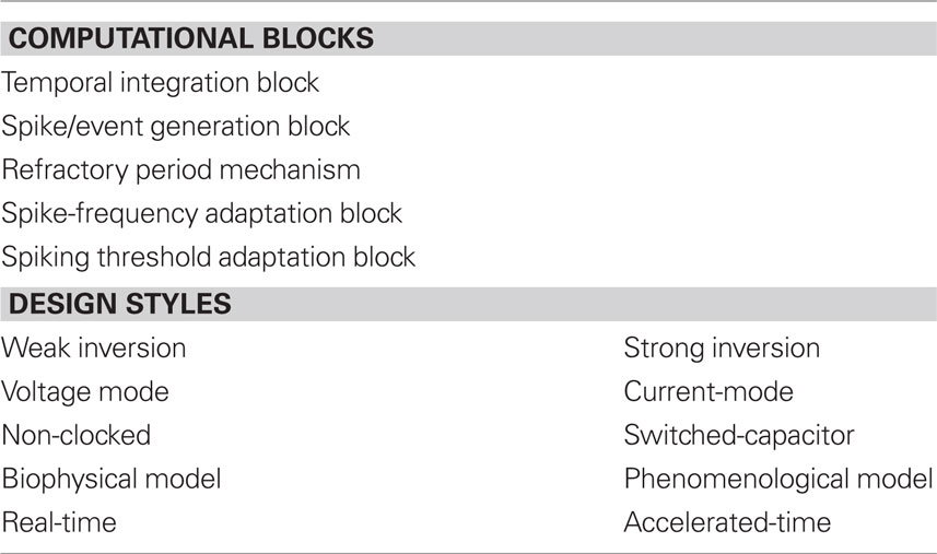
Table 1. Main SiN computational blocks, and circuit design styles.
In the next Section we will describe some of the more common circuits used as basic building blocks for building SiNs which cover all design strategies outlined in Table 1.
3 Silicon Neuron Circuit Blocks
3.1 Conductance Dynamics
Temporal integration
It has been shown that an efficient way of modeling neuron conductance dynamics and synaptic transmission mechanisms is by using simple first-order differential equations of the type  where y represents an output voltage or current, and x the input driving force (Destexhe et al., 1998). For example, this equation governs the behavior of all passive ionic channels found in nerve membranes. In the classical silicon neuron implementation proposed by Mahowald and Douglas (1991) the circuit used to implement the equation described above for modeling the neuron’s passive leak conductance is the follower–integrator circuit. The follower–integrator comprises a transconductance amplifier configured in negative feedback mode with its output node connected to a capacitor. When used in the weak-inversion domain, as a voltage mode circuit, the follower–integrator behaves as a first-order low-pass filter with a tunable conductance. A detailed description of this circuit is provided in Liu et al. (2002). Conversely, in current-mode designs, an efficient strategy for implementing the first-order differential equations described above, is to use log-domain circuits (Tomazou et al., 1990). For example, the log-domain “Bernoulli-Cell” is a circuit that can implement synaptic and conductance dynamics (Drakakis et al., 1997). The circuit operates in current-mode and in the weak-inversion (or sub-threshold) domain. It has been fully characterized in Drakakis et al. (1997), and has been used to implement Hodgkin–Huxley VLSI models of neurons (Toumazou et al., 1998). A similar log-domain circuit is shown in Figure 1A: This circuit, called the “Tau-Cell,” was first proposed in Edwards and Cauwenberghs (2000) as a BiCMOS log-domain filter; it was fully characterized in van Schaik and Jin (2003) as a sub-threshold log-domain circuit, and used in Yu and Cauwenberghs (2010b) to implement conductance-based synapses. This circuit is used also in the tau-cell neuron, described in Section 4.2. Another sub-threshold log-domain circuit is the low pass filter (LPF) described in Arthur and Boahen(2004, 2007), and shown in Figure 1B. This circuit is based on the standard log-domain low pass filter (Frey, 1993) originally implemented using bipolar transistors, but has been simplified to act as a voltage pulse integrator: Input voltage pulses (spikes) arriving at the Vin node are integrated to produce an output current Isyn with exponential rise and decay temporal dynamics. The circuit time-constant can be set by adjusting the Vτ bias, and the maximum current amplitude (e.g., corresponding to synaptic efficacy) depends on both Vτ and Vw. A recent current-mode circuit that implements temporal dynamics using this log-domain LPF circuit coupled to a wide-range transconductance amplifier has been proposed in Rachmuth and Poon (2008). This circuit allows robust emulation of emergent iono-neuronal dynamics, reproducing also chaotic bursting as observed in pacemaker cells. A detailed analysis of the synaptic and neural dynamics that can be obtained with the log-domain LPF circuit is presented in Bartolozzi and Indiveri (2007). In Bartolozzi and Indiveri (2007) the authors propose also additional circuits for implementing synaptic dynamics, including a novel differential pair integrator (DPI) circuit (see Figure 1C). Similar to the LPF pulse integrator, the DPI circuit integrates voltage pulses, following a current-mode approach. However, rather than using a single pFET to generate the appropriate Iw current, via the translinear principle (Gilbert, 1975), it uses a differential pair in negative feedback configuration. This allows the circuit to achieve LPF functionality with tunable dynamic conductances: Input voltage pulses are integrated to produce an output current that has maximum amplitude set by Vw, Vτ, and Vthr. In all circuits of Figure 1 the Vw bias (the synaptic weight) can be set by local circuits to implement learning and plasticity (Fusi et al., 2000; Mitra et al., 2009). However, the DPI offers an extra degree of freedom via the Vthr bias. This parameter can be used to implement additional adaptation and plasticity schemes, such as intrinsic or homeostatic plasticity (Bartolozzi and Indiveri, 2009). A complete analysis of the DPI and its modes of operation is provided in (Bartolozzi and Indiveri, 2007). The DPI will be used in Section 4.2 to implement the DPI-neuron.
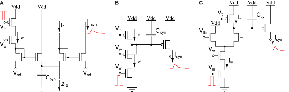
Figure 1. (A) “Tau-cell” circuit: log-domain circuit used to implement a first-order low-pass filter (LPF); (B) Sub-threshold first-order LPF circuit; (C) “DPI” circuit: non-linear current-mode LPF circuit.
Thermodynamically equivalent models
Many of the membrane channels that shape the output activity of a neuron exhibit dynamics that can be represented by state changes of a series of voltage-dependent gating particles, which must be open for the channel to conduct. The state-transitions of these particles can be understood within the context of thermodynamic equivalent models (Destexhe and Huguenard, 2000): The membrane voltage creates an energy barrier which a gating particle (a charged molecule) must overcome to change states (e.g., to open). Changes in the membrane voltage modulate the size of the energy barriers, altering the rates of opening and closing of a gating particle. The average conductance of a channel is proportional to the percentage of the population of individual channels that are open.
Since transistors also involve the movement of a charged particle through an electric field, a transistor circuit can directly represent the action of a population of gating particles (Hynna and Boahen, 2007). Figure 2 shows a thermodynamic model of a gating variable in which the drain current of transistor M2 in Figure 2A represents the gating particle’s rate of opening, while the source current of M1 represents the rate of closing. The voltage VO controls the height of the energy barrier in M2: Increasing VO increases the opening rate, shifting uV toward uH. Increasing VC has the opposite effect: The closing rate increases, shifting uV toward uL. Generally, VO and VC are inversely related; that is, as VO increases, VC should decrease.
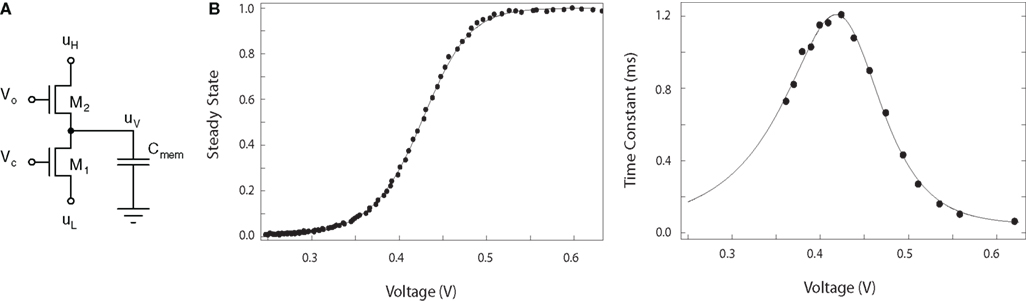
Figure 2. Thermodynamic model of a gating variable. (A) Gating variable circuit. (B) Voltage dependence of the steady-state and time-constant of the variable circuit in (A). See Hynna and Boahen (2007) for details.
The source of M2, uV is the log-domain representation of the gating variable u. Attaching uV to the gate of a third transistor (not shown) realizes the variable u as a modulation of a current set by uH. Connected as a simple activating channel – with VO proportional to the membrane voltage (Hynna and Boahen, 2007) – the voltage dependence of the steady-state and time-constant of u, as measured through the output transistor, match the sigmoid and bell-shaped curves commonly measured in neurophysiology (see Figure 2B). This circuit will be used in Section 4.1 to implement the Thalamic relay neuron.
Phenomenological models
It is also possible to model conductance and channel dynamics by abstracting their behavior, describing it with sets of differential equations, and solving them using analog circuits. One can resort to using systematic synthesis methods for mapping non-linear differential equations onto analog circuits. For example, using this strategy it was possible to design circuit implementations for the FitzHugh-Nagumo neuron model (FitzHugh, 1961), as proposed in Linares-Barranco et al. (1991). These methods typically use voltage mode above-threshold circuits rather than the current-mode sub-threshold circuits described above, and integrators are typically implemented using classical filter design techniques or S-C techniques. Examples of integrators implemented using these design strategies are described in Section 4.4.
3.2 Spike-Event Generation
Biophysically realistic implementations of neurons produce analog waveforms that are continuous and smooth in time, even for the generation of action potentials (we will describe examples of these types of circuits in Section 4.1). In many other neuron models, however, the action potential is a discontinuous and discrete event which is generated whenever a set threshold is crossed.
One of the original circuits proposed for generating discrete events in VLSI implementations of silicon neurons is the Axon-Hillock circuit (Mead, 1989). Figure 3A shows a schematic diagram of this circuit. The amplifier block A is typically implemented using two inverters in series. Input currents Iin are integrated on the membrane input capacitance Cmem, and the analog voltage Vmem increases linearly until it reaches the amplifier switching threshold (see Figure 3B). At this point Vout quickly changes from 0 to Vdd, switching on the reset transistor and activating a positive feedback through the capacitor divider implemented by Cmem and the feedback capacitor Cfb. If the reset current set by Vpw is larger then the input current, the membrane capacitor is discharged, until it reaches the amplifier’s switching threshold again. At this point Vout swings back to 0 and the cycle repeats. The inter-spike interval tL is inversely proportional to the input current, while the pulse duration period tH depends on both the input and reset currents. A comprehensive description of the circuit operation is presented in Mead (1989).
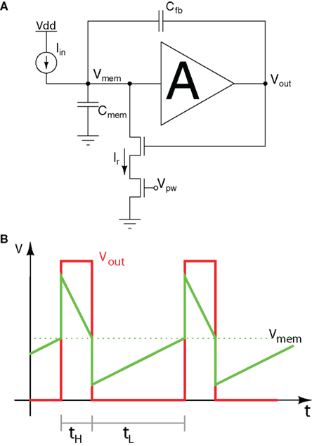
Figure 3. Axon-hillock circuit. (A) Schematic diagram; (B) Membrane voltage and output voltage traces over time.
One of the main advantages of this self-resetting neuron circuit are its excellent matching properties: mismatch is mostly dependent on the matching properties of the two capacitors of the circuit rather than any of its transistors. As low mismatch is especially desirable in imagers and photoreceptor arrays, this circuit has been applied to the design of a spiking (or event-based) vision sensor (Azadmehr et al., 2005; Olsson and Häfliger, 2008). In this case, rather than using the reset voltage Vpw as an analog bias, the designers used it as a digital signal externally controlled, and exploited its good matching properties.
3.3 Spiking Thresholds and Refractory Periods
The Axon-Hillock circuit produces a spike event when the membrane voltage crosses a voltage threshold that depends on the geometry of the transistors and on the VLSI process characteristics. In order to have better control over the spiking threshold, it is possible to use a five-transistor amplifier, as shown in Figure 4A. This neuron circuit, originally proposed in (van Schaik, 2001) comprises circuits for both setting explicit spiking thresholds and implementing an explicit refractory period. Figure 4B depicts the various stages that the membrane potential Vmem is involved in, during the generation of an action potential.
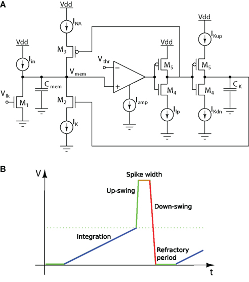
Figure 4. Voltage-amplifier I&F neuron. (A) Schematic diagram; (B) Membrane voltage trace over time.
The capacitance Cmem of this circuit models the membrane of a biological neuron, while the membrane leakage current is controlled by the gate voltage Vlk, of an nFET. In the absence of any input the membrane voltage will be drawn to its resting potential (ground, in this case), by this leakage current. Excitatory inputs (e.g., modeled by Iin) add charge to the membrane capacitance, whereas inhibitory inputs (not shown) remove charge from the membrane capacitance. If an excitatory current larger than the leakage current is injected, the membrane potential Vmem will increase from its resting potential. The voltage Vmem is compared with the threshold voltage Vthr, using a basic transconductance amplifier (Liu et al., 2002). If Vmem exceeds Vthr, an action potential is generated. The generation of the action potential happens in a similar way as in the biological neuron, where an increased sodium conductance creates the upswing of the spike, and a delayed increase of the potassium conductance creates the downswing. In the circuit this is modeled as follows: As Vmem rises above Vthr, the output voltage of the comparator will rise to the positive power supply. The output of the following inverter will thus go low, thereby allowing the sodium current INa to pull up the membrane potential. At the same time however, a second inverter will allow the capacitance CK to be charged at a speed which can be controlled by the current IKup. As soon as the voltage on CK is high enough to allow conduction of the nFET M2, the potassium current IK will be able to discharge the membrane capacitance. Two different potassium channel currents govern the opening and closing of the potassium channels: The current IKup controls the spike width, as the delay between the opening of the sodium channels and the opening of the potassium channels is inversely proportional to IKup. If Vmem now drops below Vthr, the output of the first inverter will become high, cutting off the current INa. Furthermore, the second inverter will then allow CK to be discharged by the current IKdn. If IKdn is small, the voltage on CK will decrease only slowly, and, as long as this voltage stays high enough to allow IK to discharge the membrane, it will be impossible to stimulate the neuron for Iex values smaller than IK. Therefore IKdn controls the refractory period of the neuron.
The principles used by this design to control spiking thresholds explicitly have been used in analogous SiN implementations (Indiveri, 2000; Indiveri et al., 2001; Liu et al., 2001). Similarly, the principle of using starved inverters1 and capacitors to implement refractory periods is used also in the DPI neuron described in Section 4.2.
An additional advantage that this circuit has over the Axon-Hillock circuit is power consumption: The Axon-Hillock circuit non-inverting amplifier, comprising two inverters in series, dissipates large amounts of power for slowly varying input signals, as the first inverter spends a significant amount of time in its fully conductive state (with both nFET and pFET conducting) when its input voltage Vmem slowly crosses the switching threshold. The issue of power consumption has been addressed also in other SiN designs, and will be discussed in Section 4.1.
3.4 Spike-Frequency Adaptation and Adaptive Thresholds
Spike-frequency adaptation is a mechanism observed in a wide variety of neural systems. It acts to gradually reduce the firing rate of a neuron in response to constant input stimulation. This mechanism may play an important role in neural information processing, and can be used to reduce power consumption and bandwidth usage in VLSI systems comprising networks of silicon neurons.
There are several processes that can produce spike-frequency adaptation. Here we will focus on the neuron’s intrinsic mechanism which produces slow ionic currents with each action potential that are subtracted from the input. This “negative feedback mechanism” has been modeled differently in a number of SiNs.
The most direct way of implementing spike-frequency adaptation in a SiN is to integrate the spikes produced by the SiN itself (e.g., using one of the filtering strategies described in Section 3.1) and subtract the resulting current from the membrane capacitance. This would model the effect of calcium-dependent after-hyperpolarization potassium currents present in real neurons (Connors et al., 1982) and introduce a second slow variable in the model, in addition to the membrane potential variable, that could be effectively used to produce different spiking behaviors. Figure 5A shows measurements from a SiN with this mechanism implemented (Indiveri, 2007), in response to a constant input current.
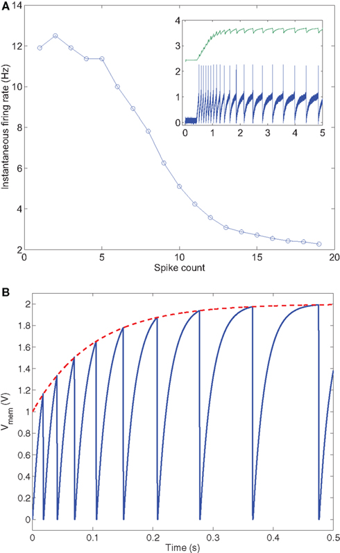
Figure 5. Spike-frequency adaptation is a SiN. (A) Negative slow ionic current mechanism: The plot shows the instantaneous firing rate as a function of spike count. The inset shows how the individual spikes increase their inter-spike interval, with time. Figure adapted from Indiveri et al. (2010). (B) Adaptive threshold mechanism: The neuron’s spiking threshold increases with every spike, therefore increasing the inter-spike interval with time.
Spike-frequency adaptation and other more complex spiking behaviors can also be modeled by implementing models with adaptive thresholds, as in the Mihalas–Niebur neuron model (Mihalas and Niebur, 2009). In this model a simple first-order equation is used to update the neuron’s spiking threshold voltage based on the membrane voltage variable itself: For high membrane voltage values, the spiking threshold adapts upwards, increasing the time between spikes for a constant input. Low membrane voltage values, on the other hand, result in a decrease of the spiking threshold voltage. The speed at which the threshold adapts in this model is dependent on several parameters. Tuning of these parameters determines the type of spiking behavior that is exhibited by the SiN. Figure 5B shows spike-frequency adaptation using an adaptive threshold. Here each time the neuron spikes the threshold voltage resets to a higher value so that the membrane voltage must grow by a larger amount and hence the time between spikes increases.
Examples of two-state variable SiNs that use either of these mechanisms will be presented in Section 4.
3.5 Axons and Dendritic Trees
Recent experimental evidence suggests that individual dendritic branches can be considered as independent computational units. A single neuron can act as a multi-layer computational network, with the individually separated dendritic branches, allowing for parallel processing of different sets of inputs on different branches before their outputs are combined (Mel, 1994).
Early VLSI dendritic systems included the passive cable circuit model of the dendrite specifically by implementing the dendritic resistance using S-C circuits (Elias and Northmore, 1999; Rasche and Douglas, 2001). Other groups have subsequently incorporated some active channels into VLSI dendritic compartments [e.g., (Arthur and Boahen, 2004)]. Farquhar and Hasler applied their transistor channel approach for building ion channels (Farquhar et al., 2004) to building active dendrite models in which ions were able to diffuse both across the membrane and axially along the length of the dendrite (Hasler et al., 2007). They used sub-threshold MOSFETs to implement the conductances seen along and across the membranes and model diffusion as the macro-transport method of ion flow. The resulting single dimensional circuit is analogous to the diffuser circuit described in Hynna and Boahen (2006), but allows the conductances of each of the MOSFETs to be individually programmed to obtain the desired neuron properties. In Hasler et al. (2007) they showed how an aVLSI active dendrite model could produce action potentials down a cable of uniform diameter with active channels every five segments.
The authors in Wang and Liu (2010) have recently constructed an aVLSI neuron with a reconfigurable dendritic architecture which includes both individual computational units and a different spatial filtering circuit (see Figure 6). Using this VLSI prototype, they demonstrate that the response of a dendritic component can be described as a non-linear sigmoidal function of both input temporal synchrony and spatial clustering (Wang and Liu, 2010). This response function means that linear or non-linear computation in a neuron can be evoked depending on the input spatio-temporal pattern.
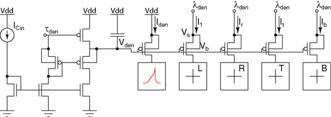
Figure 6. Dendritic membrane circuit and cable circuit connecting the compartments. The “+” blocks indicate neighboring compartments. The block to which Iden flows into is similar to the circuit in Figure 2A.
3.6 Additional Useful Building Blocks
Digi-MOS
Circuits that operate like a MOS transistor but with a digitally adjustable size factor W/L are very useful in neuromorphic SiN circuits, for providing a weighted current or for calibration to compensate for mismatch. Figure 7 shows a possible circuit implementation based on MOS ladder structures (Linares-Barranco et al., 2003). In this example, the five-bit control word b4b3b2b1b0 is used to set the effective (W/L)eff ratio. As the currents flowing through each sub-branch differ significantly, this circuit does not have unique time-constants. Furthermore small currents flowing through the lower bit branches will settle to a steady state value very slowly, therefore such a circuit should not be switched at high-speeds, but should rather be used to provide DC biasing currents. This circuit has been used in spatial contrast retinas [18] and charge packet I&F neurons within event-based convolution chips (Serrano-Gotarredona et al., 2006, 2008) for mismatch calibration.
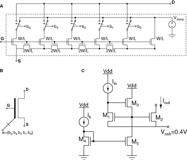
Figure 7. (A) Digi-MOS: MOS transistor with digitally adjustable size factor (W/L)eff. Example five-bit implementation using MOS ladder techniques (B) Digi-MOS circuit symbol; (C) Very low current mirror: Circuit with negative gate-to-source voltage biasing for copying very low currents.
Alternative design schemes, using the same principle but different arrangement of the transistors can be used for applications in which high-speed switching is required (Leñero-Bardallo et al., 2010).
Very low current mirrors
Typically, the smallest currents that can be processed in conventional circuits are limited by the MOS “off sub-threshold current,” which is the current a MOS transistor conducts when its gate-to-source voltage is zero. However, MOS devices can operate well below this limit (Linares-Barranco and Serrano-Gotarredona, 2003). To make MOS transistors operate properly below this limit, one needs to bias them with negative gate-to-source voltages, as illustrated in the current mirror circuit of Figure 7C. Transistors M1–M2 form the current mirror. Current Iin is assumed to be very small (pico or femto amperes), well below the “off sub-threshold current.” Consequently, transistors M1 and M2 require a negative gate-to-source voltage. By using the voltage level shifter M4–M5 and connecting the source voltage of M1–M2 to Vnsh = 0.4 V, the mirror can be biased with negative gate-to-source voltages. This technique has been used to build very low frequency compact oscillators and filters (Linares-Barranco and Serrano-Gotarredona, 2003), or to perform in-pixel direct photo current manipulations in spatial contrast retinas (Costas-Santos et al., 2007).
4 Silicon Neuron Implementations
We will now make use of the circuits and techniques introduced in Section 3 to describe silicon neuron implementations. We organized the various circuit solutions in the following way: sub-threshold biophysically realistic models; compact I&Fcircuits for event-based systems; generalized I&F neuron circuits; above threshold, accelerated-time, S-C, and digital designs.
4.1 Sub-Threshold Biophysically Realistic Models
The types of SiN designs described in this section exploit the biophysical equivalence between the transport of ions in biological channels and charge carriers in transistor channels. In the classical conductance-based SiN implementation described in Mahowald and Douglas (1991), the authors modeled ionic conductances using five-transistor transconductance amplifier circuits (Liu et al., 2002). In Farquhar and Hasler (2005), the authors showed how it is possible to model ionic channels using single transistors, operated in the sub-threshold domain. By using two-transistor circuits Hynna and Boahen (2007) showed how it is possible to implement complex thermodynamic models of gating variables (see also Section 3.1). By using multiple instances of the gating variable circuit of Figure 2A it is possible, for example, to build biophysically faithful models of thalamic relay neurons.
The thalamic relay neuron
Thalamic relay neurons possess a low-threshold calcium channel (also called a T-channel) and a slow inactivation variable, which turns off at higher voltages and opens at low voltages. The T-channel can be implemented using a fast activation variable, and implemented using the gating variable circuit of Figure 2. Figure 8A shows a simple two-compartment neuron circuit with a T-channel current, which can reproduce many response properties of real Thalamic relay cells (Hynna and Boahen, 2009). In the neuron circuit of Figure 8A the first block (on the left) integrates input spikes and represents the dendritic compartment, while the second block (on the right) produces output voltage spikes, and represents the somatic compartment.
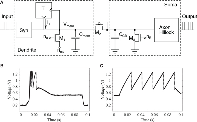
Figure 8. Two-compartment Thalamic relay neuron model. (A) Neuron circuit. (B,C) Dendritic voltage (Vmem) measurements of the relay cell’s two response modes: burst (B) and tonic (C). An 80-ms wide current step is injected into the dendritic compartment at 10 ms in both cases.
The dendritic compartment contains all active membrane components not involved in spike generation – namely, the synapses (e.g., one of the low-pass filters described in Section 3.1) and the T-channel – as well as common passive membrane components – a membrane capacitance (Cmem) and a membrane conductance (the nFET M1).
The somatic compartment, comprising a simple I&F neuron such as the Axon-Hillock circuit described in Section 3.2, receives input current from the dendrites through a diode-connected transistor (M2). Though a simple representation of a cell, relay neurons respond linearly in frequency to input currents (McCormick and Feeser, 1990), just as an I&F cell. Due to the rectifying behavior of the diode (the pFET M2 in Figure 8A), current only passes from the dendrite to the soma. As a result, the somatic action potential does not propagate back to the dendrite; only the hyperpolarization (reset) that follows is evident in the dendritic voltage trace (Vmem). This is a simple approximation of dendritic low-pass filtering of the back-propagating signal.
When Vmem rests at higher voltages, the T-channel remains inactivated, and a step change in the input current simply causes the cell to respond with a constant frequency (see Figure 8C). If an inhibitory current is input into the cell, lowering the initial membrane voltage, then the T-channel deactivates prior to the step (see Figure 8B). Once the step occurs, Vmem begins to slowly increase until the T-channel activates, which excites the cell and causes it to burst. Since Vmem is now much higher, the T-channel begins to inactivate, seen in the decrease of spike frequency within the burst on successive spikes, leading eventually to a cessation in spiking activity. In addition to the behavior shown here, this simple model also reproduces the Thalamic response to sinusoidal inputs (Hynna and Boahen, 2009).
The approach followed for this Thalamic relay SiN can be extended by using and combining multiple instances of the basic building blocks described in Section 3.1.
A sub-threshold Hodgkin–Huxley based neuron
In Yu and Cauwenberghs (2010a) the authors proposed a sub-threshold Hodgkin–Huxley (H–H) based SiN model by combining instances of the tau-cell circuit shown in Figure 1 with sub-threshold circuits of the type shown in Figure 9, which implement the non-linear functions typically used with the H–H model gating variables m, h, and n (Hodgkin and Huxley, 1952). Specifically, in Yu and Cauwenberghs (2010a) the authors presented a mixed-signal VLSI chip integrating a biophysical network of four H–H neurons and twelve conductance-based synapses, with programmable detailed kinetics of channel gating variables. The voltage dependence profile of closing and opening rates for each of the 24 channel gating variables are individually digitally programmable using on-chip digital-to-analog converters (DACs) and analog spline regression functions implemented with the seven-point additive spline (Yu and Cauwenberghs, 2010a) sigmoidal function circuit of Figure 9. Tau-cell based dynamic and cascaded translinear circuits (Figure 1A) implement first-order rate kinetics in the channel variables and their non-linear gating of the corresponding membrane channel conductances. The comparison between the experimental silicon and modeled (experimental neuroscience) equilibrium values of the channel gating variables is given in Figure 9B. The temporal scale of the dynamics both in the membrane and the channel variables can be uniformly scaled, for a global speedup of the analog simulation, by tuning a single current bias parameter (Yu and Cauwenberghs, 2010a).
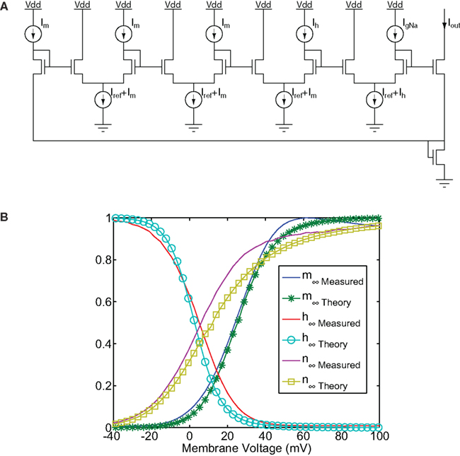
Figure 9. (A) Translinear circuit implementing gated conductances of the form x3yg used to implement H–H conductance equations (Hodgkin and Huxley, 1952). (B) Steady-state (in)activation functions measured on the sub-threshold H–H neuron (figure adapted from Yu and Cauwenberghs, 2010a).
4.2 Compact Integrate-and-Fire Circuits for Event-Based Systems
We have shown examples of circuits used to implement faithful models of spiking neurons. These circuits can require significant amounts of silicon real-estate. At the other end of the spectrum are compact circuits that implement basic models of I&F neurons. A common goal is to integrate very large numbers of these circuits on single chips to create large arrays of spiking elements, or large networks of neurons densely interconnected (Merolla et al., 2007; Vogelstein et al., 2007; Schemmel et al., 2008). In these systems, the strategy used to transmit spikes off-chip is to use the address-event representation (AER; Lazzaro et al., 1993; Deiss et al., 1998; Boahen, 2000): Each spiking neuron is assigned an address and when a neuron fires its address is instantaneously put on a digital bus, using asynchronous digital circuits that map and route the spikes to other nodes on different chips (Chicca et al., 2007; Schemmel et al., 2008). In this representation time represents itself, and analog signals are encoded by the inter-spike intervals between the addresses of their sending neurons. It is therefore important to develop compact low-power circuits that implement useful abstractions of real neurons, but that can also produce very fast digital pulses required by the asynchronous circuits that manage the AER communication infrastructure.
A common application of basic I&F spiking circuits is their use in neuromorphic vision sensors. In this case the neuron is responsible for encoding the signal measured by the photoreceptor, and transmitting it off-chip using the AER. In Azadmehr et al. (2005) and Olsson and Häfliger (2008), the authors used the Axon-Hillock circuit described in Section 3.2 to produce AER events. In Olsson and Häfliger (2008) the authors showed how this circuit can be interfaced to the AER interfacing circuits in a way to minimize device mismatch. Conversely, in Culurciello et al. (2003) the authors developed an imager inspired by the octopus retina, in which the spiking neuron circuit was optimized for minimum power consumption. In Lichtsteiner et al. (2008), the authors developed a retina for sensing changes in brightness, using a compact ON/OFF neuron with good threshold matching properties.
The octopus retina neuron
The neuron used in the octopus retina (Culurciello et al., 2003) is shown in Figure 10. As mentioned in Section 3.2, any neuron that uses inverters (starved or otherwise) will allow the short-circuit current between Vdd and ground (GND) to flow when the transistors are both on and in saturation, which is the case at threshold. This is further compounded by the fact that the membrane potential usually changes very slowly, on time scales of milliseconds to seconds, which means that the spike generator remains in the high power consumption regime. Positive feedback, either capacitive- or current-based, can accelerate its transition. Capacitive feedback is already used in the Axon-Hillock circuit, however current-based feedback is more effective for reducing power consumption. Hence the octopus neuron has four interesting properties: (1) It uses current feedback to accelerate the membrane potential transition when threshold is reached by adding an additional input current to the neuron. (2) It efficiently re-uses the short-circuit current in the spike generator to generate the feedback current. (3) The membrane capacitor (Cmem of Figure 10) is not completely discharged to GND during spike production by disconnecting it from the feedback current and the input of the spike generator. The input of the spike generator, however, accelerates to Gnd. This reduces power during spike production by a factor of approximately 25, accelerates the transition at threshold by a factor of approximately 100, and reduces power consumption during reset (Culurciello et al., 2003). (4) It only consumes power during spike generation and reset, which typically lasts for a few nano-seconds. The net effect is a total energy consumption of less than 4 pJ/spike in the 0.6 μm CMOS process in which the chip was implemented.
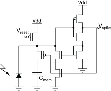
Figure 10. The octopus retina neuron. The input current is generated by a photodetector, while the spike generator uses positive current feedback to accelerate input and output transitions to minimize short-circuit currents during spike production. The membrane capacitance (Cmem) is disconnected from the input of the spike generator to further accelerate transition and to reduce power during reset.
The dynamic vision sensor differencing neuron
Another compact neuron circuit is the one used in the dynamic vision sensor (DVS) silicon retina (Lichtsteiner et al., 2008). This circuit is optimized to reduce mismatch across cells. The DVS has pixels that produce an ON or OFF event signifying quantized increases and decreases of log intensity since the last event from the pixel. In the DVS, the input to the ON/OFF neuron comes from a logarithmic photoreceptor, but this same circuit could be used with any input that can drives the capacitive input. This circuit is nearly a perfect integrator: The corner frequency is about 0.05 Hz and is limited by the off-state leakage of the reset transistor. The pixel circuit is shown in Figure 11. Each time the pixel outputs an event (either ON or OFF), a reset pulse from the AER communication circuits memorizes the last log intensity value across capacitor C1. Changes in log intensity are capacitively coupled to the input of the inverting capacitive-feedback amplifier A1, which has a gain of about −20. The A1 output Vd1 is then compared to two reference levels by the high gain amplifiers AON and AOFF. When VON or VOFF crosses the logic threshold, transmission of the ON or OFF event is initiated, resulting finally in a pulse on Vreset that starts the cycle over again.
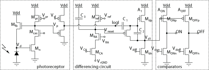
Figure 11. Dynamic vision sensor (DVS) complementary ON–OFF differencing neuron. ON and OFF events are produced by quantized increases and decreases of log intensity since the last event from the pixel. The ON/OFF events are reset by row and column acknowledge signals VCA and VRA, which produces a reset pulse of a duration controlled by Vrefr. The mismatches in the comparator thresholds of ≈20 mV is reduced by a factor of the gain of 20 in the switched-capacitor differencing amplifier, resulting in an effective threshold mismatch of about 1 mV at Vp.
The matching behavior of this circuit is the key to the success of the DVS, which is the first event-based silicon retina that has been commercialized and sold to other institutions. Because the DC mismatch in the log intensity value is blocked by C1, and because A1 inserts a high gain element that appears before the poorly matched comparators AON and AOFF, the mismatch referred back to the signal of interest (dlogI) is reduced by the gain of A1. For example, if the mismatch of AON/AOFF are 20 mV and the gain A1 = 20, then the mismatch at the logI output is reduced to 1 mV, which corresponds to a visual contrast of about 3.5%. This relatively good matching allows the DVS to be used with natural visual input, which often has rather low contrast. This circuit is an example of the general principle of removing static mismatch and amplifying before comparing for improving precision using imprecise elements. Measurements show that across an array of 16k pixels the one-sigma matching is equivalent to about 2% contrast. The five-sigma matching (which applies across a large array of cells) is then about 10%, in agreement with practical contrast threshold settings of about 15% that we routinely use (Lichtsteiner et al., 2008).
4.3 Generalized Integrate-and-Fire Neuron Circuits
The simplified I&F neuron circuits described in the previous Section require far less transistors and parameters than the biophysically realistic models of Section 4.1. But they do not produce a rich enough repertoire of behaviors useful for investigating the computational properties of large neural networks (Izhikevich, 2003; Brette and Gerstner, 2005). A good compromise between the two approaches can be obtained by implementing conductance-based or generalized I&F models (Jolivet et al., 2004). It has been shown that these types of models that capture many of the properties of biological neurons, but require less and simpler differential equations compared to H–H based models (Izhikevich, 2003; Jolivet et al., 2004; Brette and Gerstner, 2005; Mihalas and Niebur, 2009; Naud et al., 2009). In addition to being efficient computational models for software implementations, these models lend themselves to efficient hardware implementation as well (Wijekoon and Dudek, 2008; Folowosele et al., 2009a; Livi and Indiveri, 2009; Indiveri et al., 2010; Rangan et al., 2010; van Schaik et al., 2010a, 2010b).
The tau-cell neuron
The circuit shown in Figure 12, dubbed as the “Tau-Cell neuron” been used as the building block for implementations of both the Mihalas–Niebur neuron (van Schaik et al., 2010a) and the Izhikevich neuron (Rangan et al., 2010; van Schaik et al., 2010b). The basic leaky I&F functionality is implemented using the tau-cell log-domain circuit described in Section 3.1. This approach uses current-mode circuits, so the state variable, which is normally the membrane voltage, Vmem, is transformed to a current Imem. A tau-cell, configured as a first-order low-pass filter, is used to model the leaky integration. In order to create a spike, Imem is copied by pFETs M5 and M8 and compared with the constant threshold current Iθ. Since Imem can be arbitrarily close to Iθ, a current limited inverter (M12, M13) is added to reduce power consumption while converting the result of the comparison into a digital value Vnspk. A positive voltage spike Vspk is generated with inverter M14, M15 with a slight delay with respect to Vnspk. pFET M5–M7 implement positive feedback based on Vnspk while nFET M16 resets Imem to a value determined by Vel. This reset causes the end of the positive feedback and the end of the spike and the membrane is ready to start the next integration cycle.
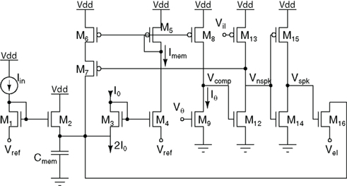
Figure 12. The tau-cell neuron circuit.
The log-domain LPF neuron
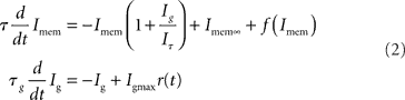
The log-domain LPF neuron (LLN) is a simple yet reconfigurable I&F circuit (Arthur and Boahen, 2004, 2007) that can reproduce many of the behaviors expressed by generalized I&F models. Based on the LPF of Figure 1B, the LLN benefits from the log-domain design style’s efficiency, using few transistors, operating with low-power (50–1000 nW), and requiring no complex configuration. The LLN realizes a variety of spiking behaviors: Regular spiking, spike-frequency adaptation, and bursting (Figure 13B). The LLN’s dimensionless membrane potential v, and adaptive conductance g variable (proportional to Iν and Ig of Figure 13A respectively), can be described by the following set of equations:
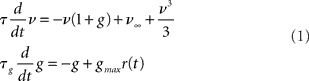
where ν∞ is v’s steady state level in the absence of positive feedback and g = 0; τ and τg are the membrane and adaptive conductance time-constants, respectively; and gmax is the adaptive conductance’s absolute maximum value. When v reaches a high level (>>10), a spike is emitted, and r(t) is set high for a brief period, TR. r(t) is a reset–refractory signal, driving v low (not shown in equation).
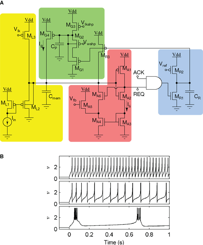
Figure 13. The log-domain LPF neuron (LLN). (A) The LLN circuit comprises a membrane LPF (yellow, ML1−3), a spike-event generation and positive-feedback element (red, MA1−6), a reset-refractory pulse generator (blue, MR1−3), and a spike-frequency adaptation LPF (green, MG1−4). (B) Recorded and normalized traces from a LLN fabricated in 0.25 μm CMOS, exhibits regular spiking, spike-frequency adaptation, and bursting (top to bottom).
The LLN is composed of four sub-circuits (see Figure 13): A membrane LPF (ML1–3), a spike event generation and positive-feedback element (MA1–6), a reset–refractory pulse generator (MR1–3), and an adaptation LPF (MG1–4). The membrane LPF realizes Iν(∝ν)’s first-order (resistor–capacitor) dynamics in response to Iin (∝ν∝). The positive-feedback element drives the membrane LPF in proportion to the cube of v, analogous to a biological sodium channel population. When the membrane LPF is sufficiently driven,  , resulting in a run-away potential, i.e., a spike. The digital representation of the spike is transmitted as an AER request (REQ) signal. After a spike (upon arrival of the AER acknowledge signal ACK), the refractory pulse generator creates a pulse, r(t) with a tunable duration. When active r(t) turns MG1 and MR3 ON, resetting the membrane LPF (toward VDD) and activating the adaptation LPF. Once activated the adaptation LPF inhibits the membrane LPF, realizing Ig (∝ g), which is proportional to spike frequency.
Implementing LLN’s various spiking behaviors is a matter of setting its biases. To implement regular spiking, we set gmax = 0 (set by MG2’s bias voltage Vwahp) and TR = 1 ms (long enough to drive v to 0, set by MR2’s bias voltage Vref). Spike-frequency adaptation can be obtained by allowing the adaptation LPF (MG1–4) to integrate the spikes produced by the neuron itself. This is done by increasing gmax and setting τg = 100 ms (i.e., by adjusting Vlkahp appropriately). Similarly, the bursting behavior is obtained by decreasing the duration of the r(t) pulse such that v is not pulled below 1 after each spike.
The DPI neuron
The DPI neuron is another variant of a generalized I&F model (Jolivet et al., 2004). This circuit has the same functional blocks used by LLN of Figure 13, but different instantiations of low-pass filters and current-based positive-feedback circuits: The low-pass filter behavior is implemented using instances of the tunable Diff-Pair Integrator circuit described in Section 3.1, while the positive feedback is implemented using the same circuits used in the Octopus Neuron of Figure 10. These are small differences from the point of view of transistor count and circuit details, but have an important effect on the properties of the SiN.
The DPI-neuron circuit is shown in Figure 14A. It comprises an input DPI filter (ML1 − ML3), a spike event generating amplifier with current-based positive feedback (MA1 − MA6), a spike reset circuit with AER handshaking signals and refractory period functionality (MR1 − MR6), and a spike-frequency adaptations mechanism implemented by an additional DPI filter (MG1 − MG6). The input DPI filter ML1 − ML3 models the neuron’s leak conductance, producing exponential sub-threshold dynamics in response to constant input currents. The integrating capacitor Cmem represents the neuron’s membrane capacitance, and the positive-feedback circuits in the spike-generation amplifier model both sodium channel activation and inactivation dynamics. The reset and refractory period circuit models the potassium conductance functionality. The spike-frequency adaptation DPI circuit models the neuron’s calcium conductance, and produces an after hyper-polarizing current (Ig) proportional to the neuron’s mean firing rate.
Figure 14. The DPI neuron circuit. (A) Circuit schematic. The input DPI low-pass filter (yellow, ML1 − ML3) models the neuron’s leak conductance. A spike event generation amplifier (red, MA1 − MA6) implements current-based positive feedback (modeling both sodium activation and inactivation conductances) and produces address-events at extremely low-power. The reset block (blue, MR1 − MR6) resets the neuron and keeps it in a reset state for a refractory period, set by the Vref bias voltage. An additional DPI filter integrates the spikes and produces a slow after hyper-polarizing current Ig responsible for spike-frequency adaptation (green, MG1 − MG6). (B) Response of the DPI neuron circuit to a constant input current. The measured data was fitted with a function comprising an exponential ∝e−t/τK at the onset of the stimulation, characteristic of all conductance-based models, and an additional exponential ∝e+t/τNa (characteristic of exponential I&F computational models; Brette and Gerstner, 2005) at the onset of the spike (Indiveri et al., 2010).
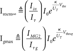
By applying a current-mode analysis to both the input and the spike-frequency adaptation DPI circuits (Bartolozzi et al., 2006; Livi and Indiveri, 2009), it is possible to derive a simplified analytical solution (Indiveri et al., 2010), very similar to the one described in Eq. (1), of the form:
where Imem is the sub-threshold current analogous to the state variable v of Eq. (1) and Ig corresponds to the slow variable g of Eq. (1) responsible for spike-frequency adaptation. The term f(Imem) accounts for the positive-feedback current Ia of Figure 14 and is an exponential function of Imem (Indiveri et al., 2010; see also Figure 14B). As for the LLN, the function r(t), is unity for the period in which the neuron spikes, and null in other periods. The other parameters in Eq. 2 are defined as: 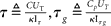 , and
, and
where  , and
, and  .
.
By changing the biases that control the neuron’s time-constants, refractory period, spike-frequency adaptation dynamics and leak behavior (Indiveri et al., 2010) the DPI-neuron can produce a wide range of spiking behaviors ranging from regular spiking to bursting.
Indeed, given the exponential nature of the generalized I&F neuron’s non-linear term f(Imem), the DPI-neuron implements an adaptive exponential I&F model (Brette and Gerstner, 2005). This I&F model has been shown to be able to reproduce a wide range of spiking behaviors, and explain a wide set of experimental measurements from pyramidal neurons (Brette and Gerstner, 2005). For comparison the LLN uses a cubic term, while the tau-cell based neuron circuits proposed in (Rangan et al., 2010; van Schaik et al., 2010b) and the quadratic and the S-C SiNs described in Section 4.4 use a quadratic term (implementing the I&F computational models proposed by Izhikevich, 2003).
4.4 Above Threshold, Accelerated-Time, Switched-Capacitor, and Digital Designs
The SiN circuits described up to now have transistors that operate mostly in the sub-threshold or weak-inversion domain, with currents ranging typically between fractions of pico to hundreds of nano-amperes. These circuits have the advantage of being able to emulate real neurons with extremely low power requirements and with realistic time-constants (e.g., for interacting with the nervous system, or implementing real-time behaving systems with time-constants matched to those of the signals they process). However, in the weak-inversion domain mismatch effects are more pronounced than in the strong-inversion regime (Pelgrom et al., 1989), and often require learning, adaptation or other compensation schemes.
It has been argued that in order to faithfully reproduce computational models simulated on digital architectures, it is necessary to design analog circuits with low mismatch and high precision (Schemmel et al., 2007). For this reason, several SiN circuits that operate in the strong-inversion regime have been proposed. In this regime however, currents are four to five orders of magnitude larger. With such currents, the active circuits used to implement resistors decrease their resistance values dramatically. As passive resistors cannot be easily implemented in VLSI to yield large resistance values, it is either necessary to use large off-chip capacitors (and small numbers of neurons per chip), to obtain biologically realistic time-constants, or to use “accelerated” time scales, in which the time-constants of the SiNs are a factor of 103 or 104 smaller than those of real neurons. Alternatively, one can use S-C for implementing small conductances (and therefore long time-constants) by moving charge in and out of integrated capacitors with clocked switches. Taking this concept one step further, one can implement SiNs using full-custom clocked digital circuits. All of these approaches are outlined in this section.
Above threshold Hodgkin–Huxley models
As mentioned in Section 4.1, Hodgkin–Huxley (H–H) conductance-based models describe faithfully the biophysics of excitable cells and are helpful to capture the main intrinsic firing and response properties of neurons. Above-threshold and bipolar circuits that implement the exact equations of Hodgkin–Huxley conductance models offer the opportunity to select and tune precisely each of the parameters appearing in the set of non-linear differential equations. These circuits need to model conductances for channels of the following types: voltage-gated, voltage and concentration-gated, passive leak, and synaptic voltage-gated. It is possible to reproduce a large variety of neural activity patterns by using a small set of bipolar and above threshold analog circuits and adjusting their parameters to represent different biophysical properties. Such types of circuits have been designed following a current-mode approach, fabricated using SiGe 0.8 and 0.35 μm technologies, and fully characterized in Renaud et al. (2007) and Saighi et al. (2011).
Figure 15A shows the schematic of the analog library circuit implementing a two-parameter sigmoidal function used to implement conductance models. As the kinetics in the circuit equations are identical to the H–H model ones, ionic currents have dynamics with biologically realistic time-constants.
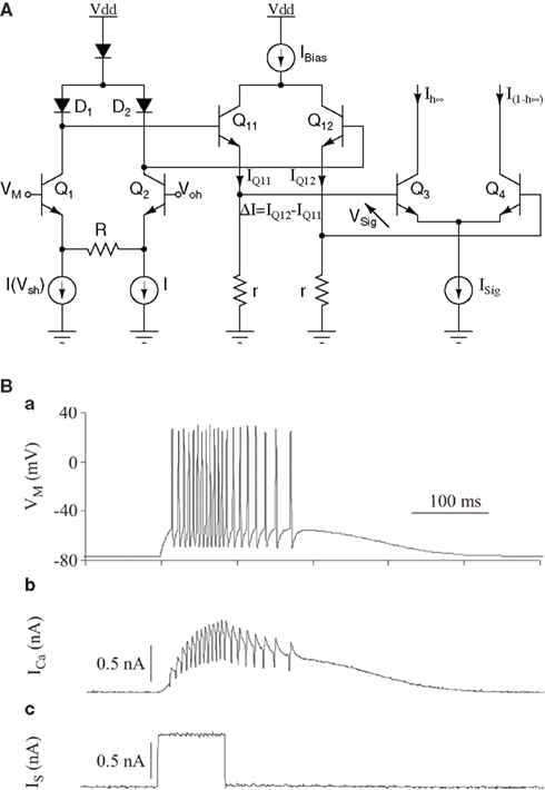
Figure 15. (A) Schematic of a “sigmoid” circuit. The Ish biasing current is set by the Vsh voltage input. From the multiplier Q1,Q2,Q11,Q12, QSig is proportional to (Vm − Voh)/Ish. From Q3−Q4 differential pair,  and
and  are complementary sigmoidal functions of Vsig, used for inactivation and activation variables, respectively. (B) A 600-ms simulation of a four-conductance silicon neuron with an input stimulation current pulse: (a) Membrane voltage Vm(t). (b) Calcium current ICa(t). (c) Stimulation current IS(t). Sodium and potassium and leak conductances generate the action potentials; a calcium conductance with a slow kinetic modulates the action potential occurrence. Individual ionic currents are available for monitoring. Voltage and current scales are the biological model scales. Hardware and biological time scales are identical, as the simulation runs in continuous and real time. When the stimulation current is applied, the neuron starts oscillating and the calcium current increases, which in turn raises the oscillation frequency. At the end of the stimulation pulse, oscillations continue until the calcium current is low enough. Finally, the neuronal activity ceases.
Each mathematical function used in the H–H neuron model, implemented using its analog equivalent circuit, is controlled by tunable analog variables which correspond to the model parameters. All parameters are stored on-chip on dynamically reconfigurable and analog DRAM cells. This implementation approach is costly in terms of silicon area and time-to-fabrication, due to the full-custom design mode and to the open parameter space that necessitates above-threshold design with bipolar and MOS transistors. To improve the design flow, the analog circuits are designed as library items which form a database. The database is used as a platform for automated design (Lévi et al., 2008): an automatic exploration process searches the database and helps a designer re-use library circuits for new designs, according to the specifications provided (e.g., from a conductance equation).
Neuron membrane voltages are obtained by summing currents chosen from a set of “generator” library circuits and summed on a capacitance representing a membrane capacitance. The currents are selected by a system of configurable switches, and a maximum of five generators can be selected for a single neuron. This covers most of the point neuron models used in computational neuroscience. External inputs and synaptic currents from pre-synaptic neurons can be injected on the membrane capacitance. The results presented in Figure 15B were measured on an VLSI chip designed using the AMS 0.35 μm SiGe technology, simulating a four-conductance model (sodium, potassium, calcium, and leak; Saighi et al., 2011). The time-constants of the activation and inactivation variables in the sodium, potassium and calcium current-models were approximated by constants. These simplifications have only minor consequences on the model’s behavior (Zou et al., 2006), as they essentially change only the shape of the spikes. These types of devices are unique tools for experiments on hybrid living–artificial neural networks. Silicon neurons represent the artificial part, connected via artificial synapses to intra- or extra-cellular electrodes to a living neural network (in vitro acute preparation or cultures). The living–artificial system acts as a single network, useful to explore cellular or synaptic mechanisms. In these types of experiments (Le Masson et al., 2002), real-time processing is mandatory to ensure a correct dialog between living and artificial neurons, and analog integrated-circuit computation simplifies the communication between the circuits and the living neurons, as the electrodes measure analog signals and inject analog currents on the living cells.
The quadratic integrate-and-fire neuron
As for the sub-threshold case, implementations of biophysically detailed models such as the one described above can be complemented by more compact implementations of simplified I&F models.
The quadratic I&F neuron circuit (Wijekoon and Dudek, 2008), shown in Figure 16A, is an example of an above-threshold generalized I&F circuit. It was inspired by the adapting quadratic I&F neuron model proposed by Izhikevich (2003). The required non-linear oscillatory behavior is achieved using differential equations of two-state variables and a separate after-spike reset mechanism, as explained in Izhikevich (2003). However, the circuit implementation does not aim to accurately replicate the non-linear equations described in Izhikevich (2003). Instead it aims at using the simplest possible circuitry of the analog VLSI implementation that can reproduce the functional behavior of the coupled system of non-linear equations.
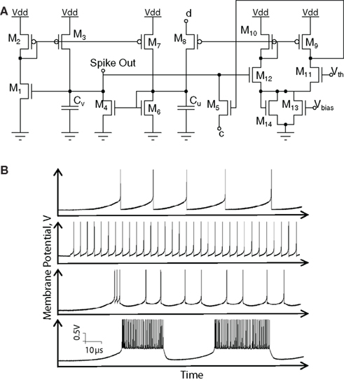
Figure 16. The Izhikevich neuron circuit (A) schematic diagram, (B) data recorded from the 0. 35 μm CMOS VLSI implementation: spiking patterns in response to input current step for various parameters of bias voltages at node c and node d: regular spiking with adaptation, fast spiking, intrinsically bursting, chattering (top to bottom).
The two-state variables, “membrane potential” (V) and “slow variable” (U), are represented by voltages across capacitors Cv and Cu respectively. The membrane potential circuit consists of transistors M1–M5 and membrane capacitor Cv. The membrane capacitor integrates post-synaptic input currents the spike-generating positive-feedback current of M3, and the leakage current generated by M4 (mostly controlled by the slow variable U). The positive-feedback current is generated by M1 and mirrored by M2–M3 and depends approximately quadratically on the membrane potential. If a spike is generated, it is detected by the comparator circuit (M9–M14), which provides a reset pulse on the gate of M5 that rapidly hyperpolarizes the membrane potential to a value determined by the voltage at node c. The slow variable circuit is built using transistors M1, M2, and M6–M8. The magnitude of the current provided by M7 is determined by the membrane potential, in a way similar to the membrane circuit. The transistor M6 provides a non-linear leakage current. The transistors and capacitances are scaled so that the potential U will vary more slowly than V. Following a membrane potential spike, the comparator generates a brief pulse to turn on transistor M8 so that an extra amount of charge, controlled by the voltage at node d, is transferred onto Cu. The circuit has been designed and fabricated in a 0.35-μm CMOS technology. It is integrated in a chip containing 202 neurons with various circuit parameters (transistor sizes and capacitances). As the transistors in this circuit operate mostly in strong inversion, the firing patterns are on an “accelerated” time scale, about 104 faster than biological real time (see Figure 16B). The power consumption of the circuit is below 10 pJ/spike. A similar circuit, but operating in weak inversion and providing spike timings on a biological time scale, has been presented in Wijekoon and Dudek (2009).
An accelerated current-controlled conductance neuron
A design that is in-between the detailed H–H neuron circuits and the quadratic neuron circuit, in terms of transistor count and circuit complexity is the above-threshold current-controlled conductance neuron.
This circuit is also an accelerated neuron model, which uses transistors operated in the strong-inversion regime to emulate the properties of neuron membrane conductances. Together with on-chip bias-generation circuits such a model can be calibrated to quantitatively reproduce numerical simulations. Figure 17A shows an exemplary neuron circuit which is part of a 100k synapse network chip (Schemmel et al., 2006). The neuron emulates three ion-channels and a spike-generation circuit consisting of a high-speed comparator using positive feedback and an adjustable refractory period.
Figure 17. Accelerated current-controlled conductance neuron. (A) Schematic diagram: excitatory and inhibitory synaptic inputs can be connected as an array of current-sinks to the Iinhib or Iexc nodes. The passive leak behavior is controlled via the Ileak node. (B) Measured response of the membrane potential to 256 Poisson distributed input spike trains, compared to an equivalent software simulation. The chip is calibrated to an acceleration factor of 104. Top: input spike trains with 8 Hz mean firing rate in biological time. Middle: membrane voltage calculated with the software simulator NEST (Eppler et al., 2008). Bottom: membrane voltage recorded from the hardware neuron.
Functionally the ion-channels are realized by current-controlled conductances. The inhibitory and excitatory channels receive a current-sum representing the total neuro-transmitter density in the synaptic cleft of the inhibitory and excitatory synapses respectively. Thereby, the time course of the synaptic conductance is generated outside of the neuron circuit and may differ for each synapse. Using a current-mode input is mandatory at the high acceleration factor of the neuron (104–105). A rise-time of 1 ms in biology translates to 10 ns. Considering a voltage swing of 1 V and a total capacitance of 5 pF for the neuron input2 the current needed is 500 μA. If the voltage swing can be limited to 20 mV, the maximum current generated by a single synapse would be reduced to a much more manageable 10 μA.
The low input impedance necessary at the neuron inputs is generated by wide cascode transistors (M6 and M9). The circuits for the leakage and the inhibitory conductances are standard operational transconductance amplifiers (OTA1 and 2). In case of the inhibitory conductance, the linear input range is extended by using a voltage-divider chain at the input of the OTA built from long transistors. This is feasible since the additional leakage generated by these transistors can be compensated by reducing the static leakage current Ileak.
The excitatory conductance has to react very quickly to changes in the input current, as shown in Figure 17B. For the post-synaptic pulse of a single synapse a current in the order of 10 μA must be sourced with a rise-time below 10 ns. Using an OTA would exceed the available silicon area and quiescent power envelope. A simple but effective solution is the usage of a current mirror (M7 and M8) with low output impedance, realized by utilizing transistors with minimum channel length. A comparison between the measured neuromorphic circuit response and a numerical simulation is shown in Figure 17B. As shown, the spike-times are in good agreement with each other. The network is in a high-conductance state throughout the stimulation.
The switched-capacitor Mihalas–Niebur neuron
Switched-capacitors have long been used in integrated circuit design to enable the implementation of variable resistors whose sizes can vary over several orders of magnitude. This technique can be used as a method of implementing resistors in silicon neurons, which is complementary to the methods described in the previous sections. More generally, S-C implementations of SiNs produce circuits whose behaviors are robust, predictable and reproducible (properties that are not always met with sub-threshold SiN implementations).
The circuit shown in Figure 18A implements a leaky I&F neuron implemented with S-Cs (Folowosele et al., 2009a). Here the post-synaptic current is input onto the neuron membrane, Vm. The S-C, SW1, acts as the “leak” between the membrane potential, Vm, and the resting potential of the neuron, EL. The value of the leak is varied by changing either the capacitor in SW1 or the frequency of the clocks φ1 and φ2. A comparator (not shown) is used to compare the membrane voltage Vm with a reset voltage Θr. Once Vm exceeds Θr a “spike” voltage pulse is issued and Vm is reset to the resting potential EL.
Figure 18. Switched-capacitor Mihalas–Niebur neuron implementation. (A) Neuron membrane circuits; (B) adaptive threshold circuits.
The Mihalas–Niebur S-C neuron (Mihalas and Niebur, 2009) is built by combining the I&F circuit of Figure 18A with the variable threshold circuit shown in Figure 18B. The circuit blocks are arranged in a way to implement the adaptive threshold mechanism described in Section 3.4. As the circuits used for realizing the membrane and the threshold equations are identical, the density of arrays of these neurons can be doubled, when simple I&F with fixed threshold properties are desired. The main drawback of this approach is the need for multiple phases of the S-C clocks which must be distributed (typically in parallel) to each neuron.
Experimental results measured from a fabricated integrated circuit implementing this neuron model (Folowosele et al., 2009b) are shown in Figure 19. The ease with which these complex behaviors can be evoked in S-C neurons, without extensive and precise tuning, demonstrates their utility in large silicon neuron arrays.
Figure 19. S-C Mihalas–Niebur neuron circuit results demonstrating 10 of the known spiking properties that have been observed in biological neurons. Membrane voltage and adaptive threshold are illustrated in blue and black respectively. (A) – tonic spiking, (B) – class 1 spiking, (C) – spike-frequency adaptation, (D) – phasic spiking, (E) – accommodation, (F) – threshold variability, (G) – rebound spiking, (H) – input bistability, (I) – integrator, (J) – hyper-polarized spiking.
The digitally modulated charge packet input neuron
The S-C principle of using discrete time and clocked signals can be extended to use high-speed pulsing current mirrors for building weight-modulated charge packet driven leaky I&F neurons.
In this framework, spikes produced by a source neuron act as asynchronous clock signals that selectively activate a set of binary weighted high-speed pulsing current mirrors at the destination neurons. The selection of which current mirror branch is activated depends on a digital word that represents the neuron’s synaptic weight. To implement the neuron leak conductance, an opposite sign pulsing current mirror is driven by spikes generated by a periodic signal from a global on chip clock. Figure 20A shows a circuit diagram representing this concept. Spikes may have a duration of down to about 100 ns for currents in the order of one nano amperes (Serrano-Gotarredona et al., 2006). This idea has been exploited to build arrays of I&F neurons in AER convolution chips (Serrano-Gotarredona et al., 2006). Each high-speed current mirror input branch is biased by a digitally calibrated current, using a digi-MOS (see Section 3.6), to compensate for transistor mismatch. Also, since the I&F neurons have to handle signed charge packages, both NMOS and PMOS high speed digitally calibrated pulsing current mirrors are required (see top and bottom part of Figure 20A). The neuron produces both positive (Pulse+) and negative (Pulse−) spikes, depending on the (excitatory or inhibitory) destination synapse, and integrates both positive and negative input pulses until it reaches corresponding positive and negative spiking thresholds. After generating an output spike, the neuron is reset to an intermediate reset level between the two thresholds. The leakage is also signed, depending on whether the actual neuron state is above or below the reset level. As both NMOS and PMOS calibrated pulsing current mirrors are available, there is no need to implement extra mirrors for the leak, but simply activate a special leak-weight when a leak-pulse (PulseF) is received. Figure 20 shows the overall neuron circuit diagram. These techniques were used in an AER convolution chip (Serrano-Gotarredona et al., 2006), for achieving an overall precision of 3 bits (plus sign). With weights and spike durations down to about 100 ns, each mirror bit branch required 5 bit calibration using transistor dimensions of 1.2/4 μm. Overall neuron size was 90 × 90 μm2 in a 0.35 μm CMOS process.
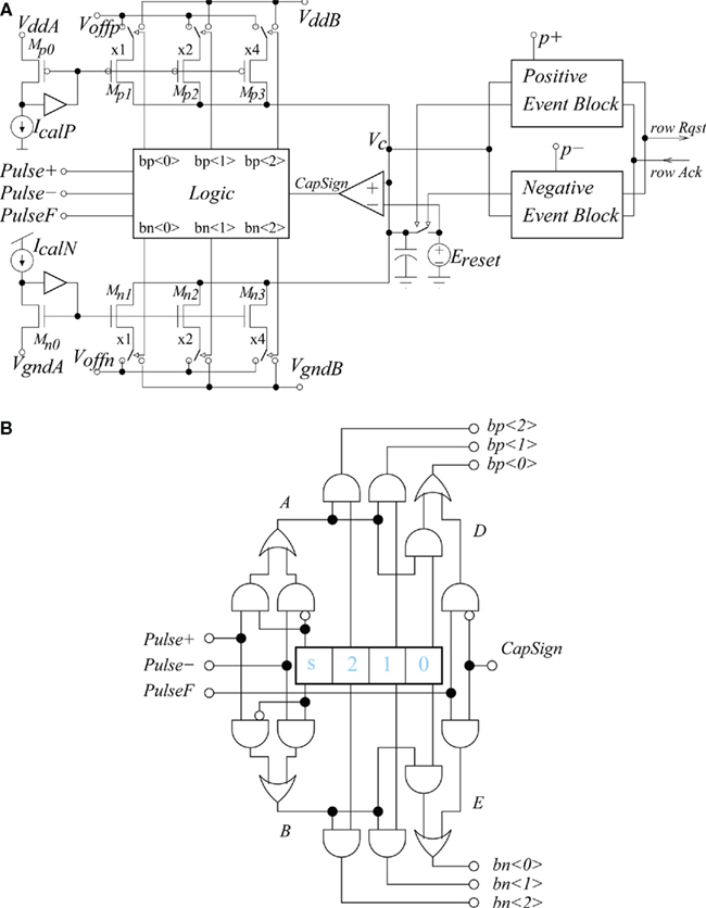
Figure 20. (A) Digitally weight-modulated and calibrated charge packet driven leaky I&F neuron schematic. The neuron handles positive and negative charge packets to emulate excitatory and inhibitory synapses, and has input for a periodic global signal PulseF to implement a programmable constant rate leak. Neuron can deliver positive or negative output events. (B) Detail of logic block in (A).
Full-custom digital I&F neuron
An alternative option requiring approximately the same area usage, but with much higher precision, is to implement the I&F neuron using all digital techniques. This idea was explored in Camuñas Mesa et al. (2008) where the authors proposed the circuit shown in Figure 21. In this implementation a digital adder and accumulator are used together with digital comparing circuits, for implementing the integration and spike-generation operations of the I&F model. Using the same technology used for the digitally modulated neuron described above, and for a similar area usage of 100 × 100 μm2, it was possible to use accumulators and adders with 18-bit precision and synaptic weights with 5-bit (plus sign) precision. The I&F leak was implemented by stimulating an inhibitory synapse with a fixed weight at a periodic global rate. In this implementation spikes can have a duration as small as 50 nano-seconds.
Figure 21. Block diagram of a fully digital I&F neuron. Calibrated current source, pulsing current mirrors, and integration capacitors of Figure 20, are replaced by digital adder and accumulator circuits.
Digital VLSI I&F neurons
Digital VLSI implementations of neurons and neural systems are also being evaluated, without resorting to full-custom VLSI designs. Examples include solutions using FPGAs (Mak et al., 2006; Cassidy and Andreou, 2008), multi-core based architectures using multiple ARM cores (Jin et al., 2010), and conventional graphical processing units (GPUs; Fidjeland et al., 2009). These approaches allow the development of large-scale spiking neural network simulations, without having to resort to powerful and power-hungry general purpose computing architectures.
5 Discussion
While the digital processing paradigm, ranging from standard computer simulations to custom FPGA designs, is advantageous for its stability, fast development times, and high precision properties, full-custom VLSI solutions can often be optimized in terms of power consumption, silicon area usage, and speed/bandwidth usage. We anticipate that future developments in large-scale neuromorphic circuits and systems designs will increasingly combine full-custom analog and synthesized digital designs, in order to optimize both core and peripheral neural and synaptic functions in a highly programmable and reconfigurable architecture. The relative merits and the right mix of analog versus digital in neuromorphic computing (Sarpeshkar, 1998) remain a subject for further investigation and will likely require highly application dependent optimization. We expect such carefully tailored combinations of silicon neurons and custom analog/digital VLSI neural networks to offer solutions to a large variety of applications, ranging from the efficient implementation of large-scale and real-time spike-based computing systems, to the implementation of compact microelectronic brain–machine interfaces. In particular, even though sub-threshold current-mode circuits are reputed to have higher mismatch than above-threshold circuits, they have lower noise energy (noise power times bandwidth), and superior energy efficiency (bandwidth over power; Sarpeshkar et al., 1993; Shi, 2009). Indeed, the sources of inhomogeneities (e.g., device mismatch) which are often considered a problem, can actually be exploited in networks of SiNs for computational purposes (similar to how real neural systems exploit noise; Chicca and Fusi, 2001; Chicca et al., 2003; Merolla and Boahen, 2004). Otherwise, sources of mismatch can be minimized at the device level with clever VLSI layout techniques (Liu et al., 2002), and at the system level by using the same strategies used by the nervous system. In particular, adaptation and learning at multiple spatial and temporal scales are important mechanisms to compensate for variability in the environment, as well as in the neural hardware operating on the environment, which includes mismatch and other sources of analog imprecision in the implementation (Cauwenberghs and Bayoumi, 1999). Furthermore, by combining the advantages of synchronous and asynchronous digital technology with those of analog circuits, it is possible to efficiently calibrate component parameters and (re)configure SiN network topologies both for single chip solutions, and for large-scale multi-chip networks (Linares-Barranco et al., 2003; Silver et al., 2007; Basu et al., 2010; Yu and Cauwenberghs, 2010a; Sheik et al., 2011).
In this paper we described some of the most common circuits and techniques used to implement silicon neurons, and described a wide range of neuron circuits that have been developed over the years, using different design methodologies and for many different application scenarios. In particular, we described circuits to implement leaky I&F neurons (Mead, 1989), adaptive threshold neurons (Mihalas and Niebur, 2009), quadratic (Izhikevich, 2003), and adaptive exponential (Brette and Gerstner, 2005) I&F neurons, as well as conductance-based and Hodgkin–Huxley models. Table 2 lists all the SiNs described, pointing out their main features and characteristics.
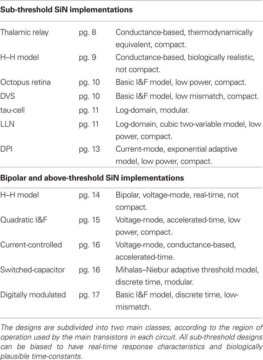
Table 2. Summary of SiN implementations described in this paper and main characteristics.
Obviously, there is no absolute optimal design. As there is a wide range of neuron types in biology, there is a wide range of design and circuit choices for SiNs. While the implementations of conductance-based models can be useful for applications in which a small numbers of SiNs are required (as in hybrid systems where real neurons are interfaced to silicon ones), the compact AER I&F neurons and log-domain implementations (such as the quadratic Mihalas–Niebur neurons, the tau-cell neuron, the LPF neuron, or the DPI neuron) can be integrated with event-based communication fabric and synaptic arrays for very large-scale reconfigurable networks. Indeed, both the sub-threshold implementations and their above-threshold “accelerated-time” counterpart are very amenable for dense and low power integration with energy efficiencies of the order of a few pico-Joules per spike (Wijekoon and Dudek, 2008; Livi and Indiveri, 2009; Rangan et al., 2010). In addition to continuous time, non-clocked sub-threshold and above-threshold design techniques, we showed how to implement SiN using digitally modulated charge packet and S-C methodologies. The S-C Mihalas–Niebur SiN circuits is a particularly robust design which exhibits the model’s generalized linear I&F properties and can produce up to ten different spiking behaviors. The specific choice of design style and SiN circuit to use depends on its application. Larger and highly configurable designs that can produce a wide range of behaviors are more amenable to research projects in which scientists explore the parameter space and compare the VLSI device behavior with that of its biological counterpart. Conversely, the more compact designs will be used in specific applications where signals need to be encoded as sequences of spikes, and where size and power budgets are critical.
The sheer volume of silicon neuron designs proposed in the literature demonstrates the enormous opportunities for innovation when inspiration is taken from biological neural systems. The potential applications span computing and biology: neuromorphic systems are providing the clues for the next generation of asynchronous, low-power, parallel computing that could breach the gap in computing power when Moore’s law runs its course, while hybrid, silicon-neuron systems are allowing neuro-scientists to unlock the secrets of neural circuits, leading one day, to fully integrated brain–machine interfaces. New emerging technologies (e.g., memristive devices) and their utility in enhancing spiking silicon neural networks must also be evaluated, as well as maintaining a knowledge-base of the existing technologies that have been proven to be successful in silicon neuron design. Furthermore, as larger on-chip spiking silicon neural networks are developed questions of communications protocols (e.g., AER), on-chip memory, size, programmability, adaptability, and fault tolerance also become very important. In this respect, the SiN circuits and design methodologies described in this paper provide the building blocks that will pave the way for these extraordinary breakthroughs.
Conflict of Interest Statement
The authors declare that the research was conducted in the absence of any commercial or financial relationships that could be construed as a potential conflict of interest.
Acknowledgments
We would like to acknowledge the reviewers for their constructive feedback. This work was supported by the EU ERC grant 257219 (neuroP), the EU ICT FP7 grants 231467 (eMorph), 216777 (NABAB), 231168 (SCANDLE), 15879 (FACETS), by the Swiss National Science Foundation grant 119973 (SoundRec), by the UK EPSRC grant no. EP/C010841/1, by the Spanish grants (with support from the European Regional Development Fund) TEC2006-11730-C03-01 (SAMANTA2), TEC2009-10639-C04-01 (VULCANO) Andalusian grant num. P06TIC01417 (Brain System), and by the Australian Research Council grants num. DP0343654 and num. DP0881219.
Footnotes
References
Arthur, J. V., and Boahen, K. (2004). Recurrently connected silicon neurons with active dendrites for one-shot learning. IEEE Int. Joint Conf. Neural Netw. 3, 1699–1704.
Arthur, J. V., and Boahen, K. (2007). Synchrony in silicon: the gamma rhythm. IEEE Trans. Neural Netw. 18, 1815–1825.
Azadmehr, M., Abrahamsen, J. P., and Hafliger, P. (2005). “A foveated AER imager chip,” in International Symposium on Circuits and Systems, ISCAS 2005, Vol. 3 (Kobe: IEEE), 2751–2754.
Bartolozzi, C., and Indiveri, G. (2007). Synaptic dynamics in analog VLSI. Neural Comput. 19, 2581–2603.
Bartolozzi, C., and Indiveri, G. (2009). Global scaling of synaptic efficacy: homeostasis in silicon synapses. Neurocomputing 72, 726–731.
Bartolozzi, C., Mitra, S., and Indiveri, G. (2006). “An ultra low power current–mode filter for neuromorphic systems and biomedical signal processing,” in Biomedical Circuits and Systems Conference, BIOCAS 2006, ed. IEEE (London, UK: IEEE), 130–133.
Basu, A., Ramakrishnan, S., Petre, C., Koziol, S., Brink, S., and Hasler, P. E. (2010). Neural dynamics in reconfigurable silicon. IEEE Trans. Biomed. Circuits Syst. 4, 311–319.
Boahen, K. A. (2000). Point-to-point connectivity between neuromorphic chips using address-events. IEEE Trans. Circuits Syst. II 47, 416–34.
Brette, R., and Gerstner, W. (2005). Adaptive exponential integrate-and-fire model as an effective description of neuronal activity. J. Neurophysiol. 94, 3637–3642.
Brette, R., Rudolph, M., Carnevale, T., Hines, M., Beeman, D., Bower, J. M., Diesmann, M., Morrison, A., Goodman, F. C., Harris, P. H. Jr., Zirpe, M., Natschläger, T., Pecevski, D., Ermentrout, B., Djurfeldt, M., Lansner, A., Rochel, O., Vieville, T., Muller, E., Davison, A. P., El Boustani, S., and Destexhe, A. (2007). Simulation of networks of spiking neurons: a review of tools and strategies. J. Comput. Neurosci. 23, 349–398.
Camuñas Mesa, L., Acosta-Jimenez, A., Serrano-Gotarredona, T., and Linares-Barranco, B. (2008). “Fully digital AER convolution chip for vision processing,” in International Symposium on Circuits and Systems, ISCAS 2008 (Seattle, WA: IEEE), 652–655.
Cassidy, A., and Andreou, A. G. (2008). “Dynamical digital silicon neurons,” in Biomedical Circuits and Systems Conference, BIOCAS 2008 (Baltimore, MD: IEEE), 289–292.
Cauwenberghs, G., and Bayoumi, M. A. editors. (1999). Learning on Silicon: Adaptive VLSI Neural Systems. Boston, MA: Kluwer.
Chicca, E., Badoni, D., Dante, V., D’Andreagiovanni, M., Salina, G., Fusi, S., and Del Giudice, P. (2003). A VLSI recurrent network of integrate–and–fire neurons connected by plastic synapses with long term memory. IEEE Trans. Neural Netw. 14, 1297–1307.
Chicca, E., and Fusi, S. (2001). “Stochastic synaptic plasticity in deterministic a VLSI networks of spiking neurons,” in Proceedings of the World Congress on Neuroinformatics, ARGESIM reports, ed. F. Rattay (Vienna: ARGESIM/ASIM Verlag) 468–477.
Chicca, E., Whatley, A. M., Dante, V., Lichtsteiner, P., Delbrück, T., Del Giudice, P., Douglas, R. J., and Indiveri, G. (2007). A multi-chip pulse-based neuromorphic infrastructure and its application to a model of orientation selectivity. IEEE Trans. Circuits Syst. I 5, 981–993.
Connors, B. W., Gutnick, M. J., and Prince, D. A. (1982). Electrophysiological properties of neocortical neurons in vitro. J. Neurophysiol. 48, 1302–1320.
Costas-Santos, J., Serrano-Gotarredona, T., Serrano-Gotarredona, R., and Linares-Barranco, B. (2007). A spatial contrast retina with on-chip calibration for neuromorphic spike-based AER vision systems. IEEE Trans. Circuits Syst. I, 54, 1444–1458.
Culurciello, E., Etienne-Cummings, R., and Boahen, K. (2003). A biomorphic digital image sensor. IEEE J. Solid State Circuits 38, 281–294.
Deiss, S. R., Douglas, R. J., and Whatley, A. M. (1998). “A pulse-coded communications infrastructure for neuromorphic systems,” in Pulsed Neural Networks, eds W. Maass and C. M. Bishop (Cambridge, MA: MIT Press), 6157–6178.
Destexhe, A., and Huguenard, J. R. (2000). Nonlinear thermodynamic models of voltage-dependent currents. J. Comput. Neurosci. 9, 259–270.
Destexhe, A., Mainen, Z. F., and Sejnowski, T. J. (1998). “Kinetic models of synaptic transmission,” in Methods in Neuronal Modelling, From Ions to Networks (Cambridge, MA: The MIT Press), 1–25.
Drakakis, E. M., Payne, A. J., and Toumazou, C. (1997). Bernoulli operator: a low-level approach to log-domain processing. Electron. Lett. 33, 1008–1009.
Edwards, R. T., and Cauwenberghs, G. (2000). Synthesis of log-domain filters from first-order building blocks. Int. J. Analog Integr. Circuits Signal Process. 22, 177–186.
Elias, J. G., and Northmore, D. P. M. (1999). “Building silicon nervous systems with dendritic tree neuromorphs,” in Pulsed Neural Networks (Cambridge, MA: IEEE), 133–156.
Eppler, J.-M., Helias, M., Muller, E., Diesmann, M., and Gewaltig, M.-O. (2008). PyNEST: a convenient interface to the NEST simulator. Front. Neuroinformatics 2:12. doi: 10.3389/neuro.11.012.2008
Farquhar, E., Abramson, D., and Hasler, P. (2004). “A reconfigurable bidirectional active 2 dimensional dendrite model,” in International Symposium on Circuits and Systems, ISCAS 2004 (Vancouver, BC: IEEE), 313–316.
Farquhar, E., and Hasler, P. (2005). A bio-physically inspired silicon neuron. IEEE Trans. Circuits Syst. 52, 477–488.
Fidjeland, A., Roesch, E. B., Shanahan, M. P., and Luk, W. (2009). “NeMo: a platform for neural modelling of spiking neurons using GPUs,” in IEEE Application-specific Systems, Architectures and Processors Conference ASAP (Boston, MA: IEEE), 137–144.
FitzHugh, N. (1961). Impulses and physiological states in theoretical models of nerve membrane. Biophys. J. 1, 445–466.
Folowosele, F., Etienne-Cummings, R., and Hamilton, T. J. (2009a). “A CMOS switched capacitor implementation of the mihalas-niebur neuron,” in Biomedical Circuits and Systems Conference, BIOCAS 2009 (Beijing: IEEE), 105–108.
Folowosele, F., Harrison, A., Cassidy, A., Andreou, A., Etienne-Cummings, A. G., Mihalas, R., Niebur, S., and Hamilton, T. J. (2009b). “A switched capacitor implementation of the generalized linear integrate-and-fire neuron,” in International Symposium on Circuits and Systems, ISCAS 2009 (Taipei: IEEE), 2149–2152.
Frey, D. R. (1993). Log-domain filtering: an approach to current-mode filtering. IEE Proc. G Circuits Device. Syst. 140, 406–416.
Fusi, S., Annunziato, M., Badoni, D., Salamon, A., and Amit, D. J. (2000). Spike–driven synaptic plasticity: theory, simulation, VLSI implementation. Neural Comput. 12, 2227–2258.
Gilbert, B. (1975). Translinear circuits: a proposed classification. Electron. Lett. 11, 14–16. See also Errata, 11, 136.
Hasler, P., Kozoil, S. S., Farquhar, E., and Basu, A. (2007). “Transistor channel dendrites implementing HMM classifiers,” in International Symposium on Circuits and Systems, ISCAS 2007 (New Orleans, LA: IEEE), 3359–3362.
Hodgkin, A. L., and Huxley, A. F. (1952). A quantitative description of membrane current and its application to conduction and excitation in nerve. J. Physiol. 117, 500–544.
Hynna, K. M., and Boahen, K. (2006). “Neuronal ion-channel dynamics in silicon,” in International Symposium on Circuits and Systems, ISCAS 2006 (Kos: IEEE), 3614–3617.
Hynna, K. M., and Boahen, K. (2007). Thermodynamically-equivalent silicon models of ion channels. Neural Comput. 19, 327–350.
Hynna, K. M., and Boahen, K. A. (2009). Nonlinear influence of T-channels in an in silico relay neuron. IEEE Trans. Biomed. Eng. 56, 1734.
Indiveri, G. (2000). Modeling selective attention using a neuromorphic analog VLSI device. Neural Comput. 12, 2857–2880.
Indiveri, G. (2007). Synaptic plasticity and spike-based computation in VLSI networks of integrate-and-fire neurons. Neural Inf. Process. Lett. Rev. 11, 135–146.
Indiveri, G., Chicca, E., and Douglas, R. (2009). Artificial cognitive systems: from VLSI networks of spiking neurons to neuromorphic cognition. Cognit. Comput. 1, 119–127.
Indiveri, G., Horiuchi, T., Niebur, E., and Douglas, R. (2001). “A competitive network of spiking VLSI neurons,” in World Congress on Neuroinformatics, ARGESIM report no. 20, ed. F. Rattay (Vienna: ARGESIM/ASIM–Verlag), 443–455.
Indiveri, G., Stefanini, F., and Chicca, E. (2010). “Spike-based learning with a generalized integrate and fire silicon neuron,” in International Symposium on Circuits and Systems, ISCAS 2010 (Paris: IEEE), 1951–1954.
Jin, X., Lujan, M., Plana, L. A., Davies, S., Temple, S., and Furber, S. (2010). Modeling spiking neural networks on SpiNNaker. Comput. Sci. Eng. 12, 91–97.
Jolivet, R., Lewis, T. J., and Gerstner, W. (2004). Generalized integrate-and-fire models of neuronal activity approximate spike trains of a detailed model to a high degree of accuracy. J. neurophysiol. 92, 959–976.
Koch, C. (1999). Biophysics of Computation: Information Processing in Single Neurons. New York: Oxford University Press.
Lazzaro, J., Wawrzynek, J., Mahowald, M., Sivilotti, M., and Gillespie, D. (1993). Silicon auditory processors as computer peripherals. IEEE Trans. Neural Netw. 4, 523–528.
Le Masson, G., Renaud, S., Debay, D., and Bal, T. (2002). Feedback inhibition controls spike transfer in hybrid thalamic circuits. Nature 4178, 854–858.
Leñero-Bardallo, J. A., Serrano-Gotarredona, T., and Linares-Barranco, B. (2010). A five-decade dynamic-range ambient-light-independent calibrated signed-spatial-contrast AER retina with 0.1-ms latency and optional time-to-first-spike mode. IEEE Trans. Circuits Syst. I 57, 2632–2643.
Lévi, T., Lewis, N., Tomas, J., and Fouillat, P. (2008). “IP-based methodology for analog design flow: application on neuromorphic engineering,” in 8th IEEE International NEWCAS Conference (Seattle, WA: IEEE), 343–346.
Lichtsteiner, P., Posch, C., and Delbruck, T. (2008). A 128 × 128 120dB 15 μs-latency asynchronous temporal contrast vision sensor. IEEE J. Solid State Circuits 43, 566–576.
Linares-Barranco, B., Sánchez-Sinencio, E., Rodrígu ez Vázquez, A., and Huertas, J. L. (1991). A CMOS implementation of FitzHugh-Nagumo neuron model. IEEE J. Solid-State Circuits 26, 956–965.
Linares-Barranco, B., and Serrano-Gotarredona, T. (2003). On the design and characterization of femtoampere current-mode circuits. IEEE J. Solid-State Circuits 38, 1353–1363.
Linares-Barranco, B., Serrano-Gotarredona, T., and Serrano-Gotarredona, R. (2003). Compact low-power calibration mini-DACs for neural massive arrays with programmable weights. IEEE Trans. Neural Netw. 14, 1207–1216.
Liu, S.-C., Kramer, J., Indiveri, G., Delbrück, T., Burg, T., and Douglas, R. (2001). Orientation-selective aVLSI spiking neurons. Neural Netw. 14, 629–643.
Liu, S.-C., Kramer, J., Indiveri, G., Delbrück, T., and Douglas, R. (2002). Analog VLSI: Circuits and Principles. Cambridge, MA: MIT Press.
Livi, P., and Indiveri, G. (2009). “A current-mode conductance-based silicon neuron for address-event neuromorphic systems,” in International Symposium on Circuits and Systems, ISCAS 2009 (Taipei: IEEE), 2898–2901.
Mak, T. S. T., Rachmuth, G., Lam, K.-P., and Poon, C.-S. (2006). A component-based FPGA design framework for neuronal ion channel dynamics simulations. IEEE Trans. Neural Syst. Rehabil. Eng. 14, 410–418.
McCormick, D. A., and Feeser, H. R. (1990). Functional implications of burst firing and single spike activity in lateral geniculate relay neurons. Neuroscience 39, 103–113.
Merolla, P., and Boahen, K. (2004). “A recurrent model of orientation maps with simple and complex cells,” in Advances in Neural Information Processing Systems, eds S. A. Solla, T. K. Leen, and K.-R. Müller Vol. 16 (Vancouver, BC: MIT Press), 995–1002.
Merolla, P. A., Arthur, J. V., Shi, B. E., and Boahen, K. A. (2007). Expandable networks for neuromorphic chips. IEEE Trans. Circuits Syst. I, 54, 301–311.
Mihalas, S., and Niebur, E. (2009). A generalized linear integrate-and-fire neural model produces diverse spiking behavior. Neural Comput. 21, 704–718.
Mitra, S., Fusi, S., and Indiveri, G. (2009). Real-time classification of complex patterns using spike-based learning in neuromorphic VLSI. IEEE Trans. Biomed. Circuits Syst. 3, 32–42.
Naud, R., Berger, T., Bathellier, B., Carandini, M., and Gerstner, W. (2009). Quantitative single-neuron modeling: competition 2009. Front. Neur. Conference Abstract: Neuroinformatics 2009, 1–8. doi: 10.3389/conf.neuro.11.2009.08.106
Olsson, J. A., and Häfliger, P. (2008). “Mismatch reduction with relative reset in integrate-and-fire photo-pixel array,” in Biomedical Circuits and Systems Conference, BIOCAS 2008, (Baltimore, MD: IEEE), 277–280.
Pelgrom, M. J. M., Duinmaijer, A. C. J., and Welbers, A. P. G. (1989). Matching properties of MOS transistors. IEEE J. Solid-State Circuits 24, 1433–1440.
Rachmuth, G., and Poon, C.-S. (2008). Transistor analogs of emergent iono-neuronal dynamics. HFSP J. 2, 156–166.
Rangan, V., Ghosh, A., Aparin, V., and Cauwenberghs, G. (2010). “A subthreshold aVLSI implementation of the Izhikevich simple neuron model,” In IEEE Engineering in Medicine and Biology Conference EMBC (Buenos Aires: IEEE).
Rasche, C., and Douglas, R. J. (2001). Forward- and backpropagation in a silicon dendrite. IEEE Trans. Neural Netw. 12, 386–393.
Renaud, S., Tomas, J., Bornat, Y., Daouzli, A., and Saïghi, S. (2007). “Neuromimetic ICs with analog cores: an alternative for simulating spiking neural networks,” in International Symposium on Circuits and Systems, ISCAS 2007 (New Orleans, LA: IEEE), 3355–3358.
Saighi, S., Bornat, Y., Tomas, J., Le Masson, G., and Renaud, S. (2011). A library of analog operators based on the hodgkin-huxley formalism for the design of tunable, real-time, silicon neurons. IEEE Trans. Biomed. Circuits Syst. 5, 3–19.
Sarpeshkar, R. (1998). Analog versus digital: extrapolating from electronics to neurobiology. Neural Comput. 10, 1601–1638.
Sarpeshkar, R., Delbrück, T., and Mead, C. A. (1993). White noise in MOS transistors and resistors. IEEE Circuits Device. Mag. 9, 23–29.
Schemmel, J., Brüderle, D., Meier, K., and Ostendorf, B. (2007). “Modeling synaptic plasticity within networks of highly accelerated I&F neurons,” In International Symposium on Circuits and Systems, ISCAS 2007 (New Orleans, LA: IEEE), 3367–3370.
Schemmel, J., Fieres, J., and Meier, K. (2008). “Wafer-scale integration of analog neural networks,” in Proceedings of the IEEE International Joint Conference on Neural Networks, Hong Kong, 431–438.
Schemmel, J., Grübl, A., Meier, K., and Muller, E. (2006). “Implementing synaptic plasticity in a VLSI spiking neural network model,” in International Joint Conference on Neural Networks (IJCNN’06) (Vancouver, BC: IEEE), 1–6.
Serrano-Gotarredona, R., Serrano-Gotarredona, T., Acosta-Jimenez, A., Serrano-Gotarredona, C., Perez-Carrasco, J. A., Linares-Barranco, A., Jimenez-Moreno, G., Civit-Ballcels, A., and Linares-Barranco, B. (2008). On real-time AER 2D convolutions hardware for neuromorphic spike based cortical processing. IEEE Trans. Neural Netw. 19, 1196–1219.
Serrano-Gotarredona, T., Serrano-Gotarredona, R., Acosta-Jimenez, A., and Linares-Barranco, B. (2006). A neuromorphic cortical-layer microchip for spike-based event processing vision systems. IEEE Trans. Circuits Syst. I 53, 2548–2566.
Sheik, S., Stefanini, F., Neftci, E., Chicca, E., and Indiveri, G. (2011). “Systematic configuration and automatic tuning of neuromorphic systems,” in International Symposium on Circuits and Systems, ISCAS 2011 (Rio de Janeiro: IEEE), 873–876.
Shi, B. E. (2009). The effect of mismatch in current-versus voltage-mode resistive grids. Int. J. Circuit Theory Appl. 37, 53–65.
Silver, R., Boahen, K., Grillner, S., Kopell, N., and Olsen, K. L. (2007). Neurotech for neuroscience: unifying concepts, organizing principles, and emerging tools. J. Neurosci. 27, 11807–11819.
Tomazou, C., Lidgey, F. J., and Haigh, D. G. (eds). (1990). Analogue IC Design: The Current-Mode Approach. Stevenage, Herts.: Peregrinus.
Toumazou, C., Georgiou, J., and Drakakis, E. M. (1998). Current-mode analogue circuit representation of Hodgkin and Huxley neuron equations. IEE Electron. Lett. 34, 1376–1377.
van Schaik, A. (2001). Building blocks for electronic spiking neural networks. Neural Netw. 14, 617–628.
van Schaik, A., and Jin, C. (2003). “The Tau-Cell: a new method for the implementation of arbitrary differential equations,” in International Symposium on Circuits and Systems, ISCAS 2003 (Bangkok: IEEE), 569–572.
van Schaik, A., Jin, C., Hamilton, T. J., Mihalas, S., and Niebur, E. (2010a). “A log-domain implementation of the Mihalas-Niebur neuron model,” in International Symposium on Circuits and Systems, ISCAS 2010 (Paris: IEEE), 4249–4252.
van Schaik, A., Jin, C., and Hamilton, T. J. (2010b). “A log-domain implementation of the Izhikevich neuron model,” in International Symposium on Circuits and Systems, ISCAS 2010 (Paris: IEEE), 4253–4256.
Vogelstein, R. J., Mallik, U., Vogelstein, J. T., and Cauwenberghs, G. (2007). Dynamically reconfigurable silicon array of spiking neurons with conductance-based synapses. IEEE Trans. Neural Netw. 18, 253–265.
Vogelstein, R. J., Tenore, F., Guevremont, L., and Etienne-Cummings, R. (2008). A silicon central pattern generator controls locomotion in vivo. IEEE Trans. Biomed. Circuits Syst. 2, 212–222.
Wang, Y., and Liu, S.-C. (2010). Multilayer processing of spatiotemporal spike patterns in a neuron with active dendrites. Neural Comput. 8, 2086–2112.
Wijekoon, J. H. B., and Dudek, P. (2008). Compact silicon neuron circuit with spiking and bursting behaviour. Neural Netw. 21, 524–534.
Wijekoon, J. H. B., and Dudek, P. (2009). “A CMOS circuit implementation of a spiking neuron with bursting and adaptation on a biological timescale,” in Biomedical Circuits and Systems Conference, BIOCAS 2009 (Beijing: IEEE), 193–196.
Yu, T., and Cauwenberghs, G. (2010a). Analog VLSI biophysical neurons and synapses with programmable membrane channel kinetics. IEEE Trans. Biomed. Circuits Syst. 4, 139–148.
Yu, T., and Cauwenberghs, G. (2010b). “Log-domain time-multiplexed realization of dynamical conductance-based synapses,” in International Symposium on Circuits and Systems, ISCAS 2010, 2558–2561 (Paris: IEEE).
Keywords: analog VLSI, subthreshold, spiking, integrate and fire, conductance based, adaptive exponential, log-domain, circuit
Citation: Indiveri G, Linares-Barranco B, Hamilton TJ, van Schaik A, Etienne-Cummings R, Delbruck T, Liu S-C, Dudek P, Häfliger P, Renaud S, Schemmel J, Cauwenberghs G, Arthur J, Hynna K, Folowosele F, Saighi S, Serrano-Gotarredona T, Wijekoon J, Wang Y and Boahen K (2011) Neuromorphic silicon neuron circuits. Front. Neurosci. 5:73. doi: 10.3389/fnins.2011.00073
Received: 15 December 2010;
Accepted: 07 May 2011;
Published online: 31 May 2011.
Edited by:
Bert Shi, The Hong Kong University of Science and Technology, Hong KongReviewed by:
Theodore Yu, University of California at San Diego, USAChi-Sang Poon, Harvard – MIT Division of Health Sciences and Technology, USA
Tadashi Shibata, University of Tokyo, Japan
Copyright: © 2011 Indiveri, Linares-Barranco, Hamilton, van Schaik, Etienne-Cummings, Delbruck, Liu, Dudek, Häfliger, Renaud, Schemmel, Cauwenberghs, Arthur, Hynna, Folowosele, Saïghi, Serrano-Gotarredona, Wijekoon, Wang and Boahen. This is an open-access article subject to a non-exclusive license between the authors and Frontiers Media SA, which permits use, distribution and reproduction in other forums, provided the original authors and source are credited and other Frontiers conditions are complied with.
*Correspondence: Giacomo Indiveri, Institute of Neuroinformatics, Swiss Federal Institute of Technology Zurich, University of Zurich, Zurich CH-8057, Switzerland. e-mail: giacomo@ini.phys.ethz.ch