 Jason R. Grenier
 Lars Brusberg2
- 1Corning Incorporated, Corning, NY, United States
- 2Corning Research & Development Corporation, Corning, NY, United States
- 3Corning Optical Communications GmbH & Co KG., Berlin, Germany
High bandwidth demanding applications such as high-performance computing and hyperscale datacenters are drivers for co-packaged optics, which aims to bring optical signals as close as possible to the electrical computing chips by integrating the electro-optic transceivers and ASICs on the same package substrate. These next-generation switches require advanced fiber-to-chip connectivity and novel packaging concepts to enable sufficient power and cost savings. As such, low-loss, high bandwidth, and high fiber-counts are required at the photonic chip interface. In this work, these challenges are addressed by enabling the multi-fiber push-on (MPO) interface at the edge of integrated glass waveguide substrates and thus leverages the existing fiber connector eco-system. An ultrafast laser process is used to singulate glass wafers into individual photonic chips leaving optical-quality end-facets with <1 μm flatness over the 6.5 mm wide connector region thereby directly enabling low-loss fiber-to-chip edge-coupling. To overcome the high-costs and complex photonic packaging associated with active alignment of the fiber connectors to the glass waveguide interfaces, ultrafast laser-ablated features are accurately positioned on the glass substrate to enable self-alignment of the MPO connector guide-pins resulting in a passive alignment approach. Subsequent mating and de-mating of the MPO connector to the glass waveguide interface yields on average a 0.19 dB increase in the coupling loss compared to using active alignment.
1 Introduction
Optical fibers form the pipeline through which voice, video, and data is transported around the globe. Every year, over 500 million kilometers of fibers are made (Jacoby, 2022) for a demanding and increasing market. Beside telecom, optical fibers are massively deployed in datacenters and high-performance computers for rack-to-rack communication. As the bandwidth needs increase, power efficient and low-cost photonic packaging is required for data switching and computing applications to save on energy and infrastructure costs. Mounting the optical transceiver on a common packaging substrate together with the electric integrated circuit (IC), so called “co-packaging of optics,” leads to fiber-to-chip connectivity inside the rack enclosure (Minkenberg et al., 2021). Waveguides in glass support advanced photonic packaging and high-density fiber-to-chip interconnects. Higher-performance ICs consume hundreds of Watts of power delivered through the printed circuit board and thus requires significant amount of heat to be efficiently dissipated by top assembled heat sinks or cold plates. As a result of the limited space between the electrical circuit board and the heat management, a low-profile edge-coupling approach to the photonic package is beneficial. In the case of edge-coupling, the optical fiber makes physical contact with the facet of the waveguide on the chip or an intermediate waveguide with a connector (Barwicz et al., 2014). Such intermediate waveguides can be made of polymer, or glass which has lower loss for O- and C-band applications.
This work focuses on providing low-loss, high fiber-count edge coupling to optoelectronic glass substrates for co-packaged optics. The advantages of using glass substrates are discussed in Section 2 along with the wafer-scale fabrication of ion-exchanged waveguides that will serves as the on-chip waveguides to which the optical fibers will couple. Section 3 presents an ultrafast laser process for the singulation of these glass wafers into individual photonic circuits, shown schematically in Figure 1A, with optical-quality end-facets (Figure 1C) around the waveguides located at the surface and within the bulk glass without any subsequent post-processing steps. Section 4 demonstrates that the major challenge of overcoming the high-costs and packaging complexities associated with multi-fiber connectivity can be met by enabling the multi-fiber push-on (MPO) interface at the edge of integrated glass waveguide substrates. Ultrafast laser-ablated features are accurately positioned on the glass substrate (Figure 1C) to enabled self-alignment of the MPO connector guide-pins resulting in a passive alignment approach for multi-fiber to chip connectivity.
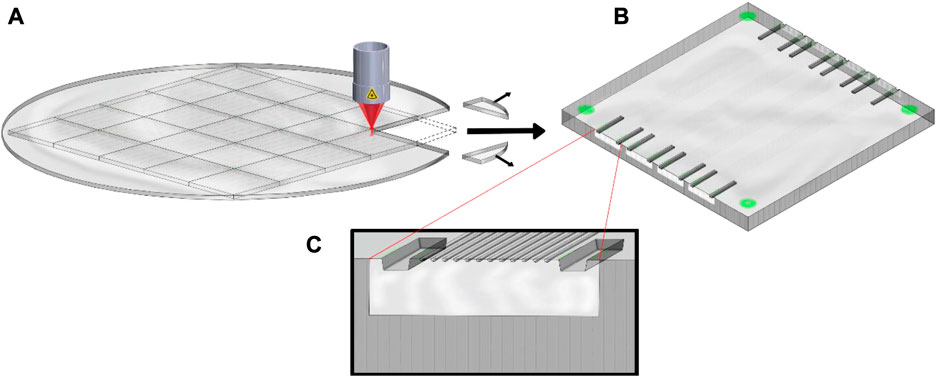
FIGURE 1. Schematic illustration of (A) the laser singulation of a glass wafer into (B) individual photonic circuits containing optical waveguides and passive alignment trenches. (C) High magnification inset of the end-facet showing the optical-quality region and alignment trenches around the ion-exchanged waveguides.
2 Glass as an optoelectronic substrate
The approach in this work consists of using an optoelectronic substrate made of glass with integrated ion-exchanged waveguides and deposited electrical redistribution lines (RDLs) on the surfaces. Integrated through glass vias (TGV) connecting the top and bottom surfaces provide power and ground to the assembled electrical and optical chips. A fully integrated glass substrate with high-speed optical and electrical interconnects provides the potential for lower packaging costs and a simpler fabrication and assembly process compared to 2.5D silicon interposer on an organic substrate or an embedded multi-die interconnect bridge (Mahajan et al., 2016) configurations. Exceptional surface smoothness along with the necessary flatness and dimensional stability for small line and space RDLs can be achieved using the fusion draw glass manufacturing process. This results in tight geometric control comparable to silicon, and far better than organic substrates (Ndip et al., 2012; Schröder et al., 2010). In contrast to silicon wafer manufacturing, glass can be formed in large sheets leading to cost effective, panel-level processing. Glass is also more rigid compared to organic materials and the coefficient of thermal expansion (CTE) is adjustable in a range between 3 and 8 ppm/°C matching silicon or between that of silicon and of organic based printed circuit boards. By matching the CTE, glass obtains low assembly warpage and improves solder joint fatigue life. For flip-chip assembly of photonic ICs, electrical and optical interfaces need to be defined for assembly. Planar integrated glass waveguides just below the glass surface can be evanescently coupled to the photonic IC by 2D fiducial alignment and flip-chip bonding in contact with the glass waveguide surface. Etching a cavity into the glass below the glass waveguide surface for the RDL and the connecting electrical bumps, enables direct contact between PIC and glass waveguide optical ports (“evanescent coupler”). Figure 2A shows an optoelectronic glass substrate with 50 μm deep cavities with TGVs.
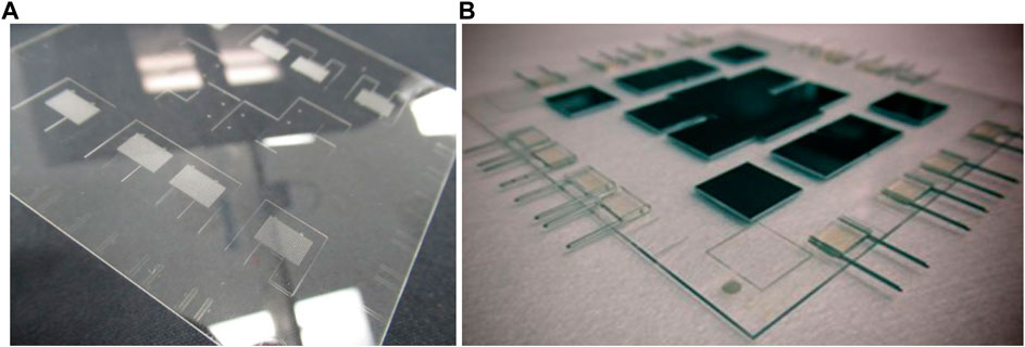
FIGURE 2. (A) Glass substrate (75 mm × 75 mm) with integrated glass waveguides, etched cavities and TGVs, and (B) an optoelectronic glass substrate with a mock-up of assembled components.
The optical waveguides are made by a multi-step process consisting of lithography, primary silver ion-exchange, fiducial protection, mask removal, secondary ion-exchange, and laser singulation. A waveguide propagation loss of less 0.1 dB/cm at wavelength of 1,310 nm was demonstrated in an alkali-containing aluminosilicate glass. The glass substrate is then connectorized with optical fibers by using edge-coupling and passive alignment of standard (e.g., MPO) optical fiber array connectors.
Figure 2B shows a novel packaging concept that consists of a glass substrate where the top redistribution layers provide high-speed electrical interconnects between high-performance electrical chips and photonic transceiver chips. A cavity is etched into the glass for embedded electrical circuitry below the glass surface. Fine-line electrical interconnects and bonding pads made of copper are defined on the floor of the etched cavity. The IOX glass waveguides are embedded close to the surface of the glass. Photonic chips with optical and electrical interfaces are flip-chip assembled and interconnected to the optical and electrical ports of the glass substrate. Such an approach is scalable to high optical port counts and can be automated by pick and place machines. The glass waveguides couple in two stages to the adiabatic tapered Si or SiN waveguide of the photonic chip to achieving mode phase matching (Brusberg et al., 2022).
3 Singulation of glass-based photonic circuits
While there are many known techniques to cut (or singulate) glass (Smirnov et al., 2011; Dudutis et al., 2020), the requirements placed on the quality and characteristics of the resulting cut edges are important considerations in the choice of the technology when applied to singulating glass-based photonic circuits. The list below outlines these characteristics.
• minimal to no chipping to avoid damaging the optical waveguides
• optical-quality and vertical end-facets to enable low-loss edge coupling
• minimal kerf width for maximum material utilization
• scalable manufacturable process in terms of throughput and cost
• ability to create free form shapes including lines that intersect, and
• sufficient edge strength to handle downstream processing and deployment in the field
One of the most common glass cutting techniques is mechanical score and break, where a score line (flaw) is created by moving a diamond scribe or score wheel across the surface of the glass (Smirnov et al., 2011). The scored edge is then placed in tension, resulting in the glass breaking along the score line. While most of the end-facet has an excellent optical-quality, the region immediately around the score line does not, as shown in the end- and top-view optical micrographs of Figures 3A, B, respectively. Unfortunately, this is exactly the area where waveguides are located. Additionally, the crack is not guided when it propagates through the bulk of the material, so the end-facet meanders along the cut and perpendicular to the cut.
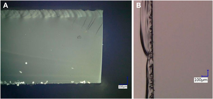
FIGURE 3. (A) End-view and (B) top-view optical micrograph of the glass edge that results from a mechanical score and break process. The score that guided the crack along the top of the image and the out of planeness from a profile view of the edge are both visible in (A).
There are also methods of cutting glass where the glass material is removed. Two common examples are diamond saw (Bondarev and Malevannyi, 1956) and water jet (Liu et al., 2019). Blade dicing using a diamond saw is an established technique where a rotary blade with tiny diamond abrasive elements embedded in it rotate to fracture and remove glass. Cutting by diamond wheel typically generates lots of damage to the glass edge and thus is slow to manage the thermal stresses in the glass and prevent unwanted fracture. Water jet cutting using water with abrasive particles added to it and is directed with high flow and pressure into a focused cutting area. As this cutting point is moved relative to the glass, the abrasive particles in the water chips away the glass slowly. These methods are typically slow, have a kerf, and do not result in a sufficient optical-quality end-facet.
There are many different lasers and laser processes that can be employed to cut glass (Nisar et al., 2013). An example of a laser process that removes material is ablation (Ashkenasi et al., 2012), which has a slow process speed that scales with the thickness of the material and yields poor quality end-facet. An example of a laser process that does not remove material is laser scoring (Du and Shi, 2003), where a focused laser beam is scanned across the surface of the glass to create a score line which is subsequently placed in tension to complete the separation. The controlled fracture technique has been demonstrated using a high-powered diode laser (Nisar et al., 2009) or a carbon dioxide (CO2) laser (Lumley, 1969) which heat the glass to a point where thermal stresses can induce a crack along which the glass is separated as the laser is scanned. While this method results in an optical-quality end-facet (Brusberg et al., 2016) the stress guiding the crack is on the millimeter scale, not micron scale, which can cause the cut to meander from the desired contour. Additionally, the stress is localized to the laser incident surface of the glass and as such, the crack at the bottom of the glass is not guided and can meander in and out of the cut plane, similar to the profile view shown above in Figure 3A.
Processing of transparent media, such as glass, has evolved significantly with the use of ultrafast laser pulses advanced both fundamental research and practical applications (Malinauskas et al., 2016). The energy of femtosecond and picosecond laser pulses can be absorbed with the bulk glass by non-linear optical processes such as multi-photon absorption and induce a localized material modification rather than a material removal (e.g., ablation). As such, laser modifications can extend through the entire thickness of the glass substrate by using, for example, laser filamentation (Hosseini and Herman, 2017) which is based on the optical Kerr effect, or quasi-non-diffracting beams, such as Bessel Beams.
3.1 Laser cutting of glass using bessel beams
A more recent advancement in the ultrafast laser cutting of glass utilizes quasi-non diffracting beams (e.g., Bessel beams) which are typically generated by an element that imparts a conical phase (e.g., axicon) to transform a Gaussian laser beam to a longitudinal focused line (Stoian et al., 2018). The length of this line can be millimeters in length and has a core diameter that is comparable to a traditional beam waist. With the development of higher pulse energy ultrafast lasers, the Bessel beam technology is an area of active research and innovations include shaping the beam to enhance cutting (Dudutis et al., 2018), creating a more desirable chamfered edge profile (Ungaro et al., 2021), and even utilizing higher order Bessel beams (Flamm et al., 2017; Baltrukonis et al., 2020).
To cut glass with ultrafast laser Bessel beams, the focal line is positioned within the body of the glass with sufficient pulse energy to create a through-body defect or modification. The focused laser beam and glass substrate are moved in relative motion to create a contour of defects which serve to guide the crack during the separation. The distance between the defects (typically 5–50 μm) and the laser frequency determines the total process speed. With a distance between defects of ∼20 microns and a laser with a high pulse repetition rate (>100 kHz), velocities of >3 m/s are possible. The key point is that the total process speed is not laser limited. The primary limitations are the ability to precisely position the glass relative to the laser and accelerating to high velocities over short distance and radiused contours. This technology has also been commercially demonstrated with fast speeds (>1 m/s) on large scales (2.2 m × 2.5 m) sheets (Terbrueggen, 2020).
From the top view one can see a crater with a crack extending to either side of the defect. When a line of defects is made, a continuous crack connects the defects as shown in Figure 4A. The laser entrance side (top of the glass) and the laser exit side (bottom of the glass) are nearly identical. If the glass is chemically or thermally strengthened, the energy stored in the glass can be sufficient to drive the crack to completion without any additional stresses. However, in cases where the glass does not have sufficient stress, external stresses can be added manually or with a second laser, such as a CO2 laser. The CO2 laser heats up the area around the defects and propagates the crack and physically separates the glass as shown in Figure 4B. The top- and end-view optical micrographs of the glass after separation are shown in Figures 4C, D, respectively. The surface roughness of the cleaved edge (Figure 4D) is generally ∼1 micron (Ra) and the planarity is of that same order.
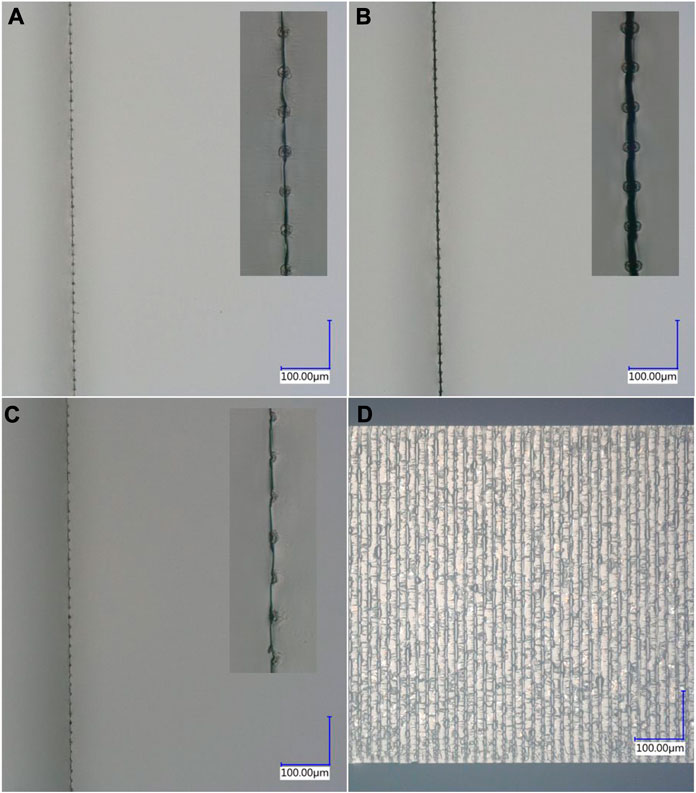
FIGURE 4. Top-view optical micrographs with magnified inset showing laser perforation line after (A) exposure to Bessel beam (B) subsequent CO2 laser exposure and (C) physically removing one side of the glass. (D) End-view optical micrograph of the laser modifications imparted by the Bessel beam cutting process.
3.2 Laser singulation of glass waveguide substrates with optical-quality end-facets
Coupling light into and out of photonics circuits is typically enabled by using grating coupling, evanescent (adiabatic) coupling, or edge coupling. High coupling efficiency, broadband coupling, and no polarization dependent loss are significant advantages of the edge coupling approach (Marchetti et al., 2019); however, it places additional requirements on the optical waveguide end-facet in order to yield low coupling loss. For example, the end-facet must be free of chips, vertical, and have a mirror-like optical-quality finish which is a significant challenge for most all glass singulation techniques. As such, the end-facets are typically polished after singulation which involves customized fixturing and several intermediate steps such as adhering, detaching, and cleaning. These steps increase the complexity, add significant costs, and can lower the overall yields.
The Bessel beam laser singulation technique described above does not result in significant chipping and produces vertical end-facets, however, the laser modifications impart a surface roughness that can scatters light. Previous research has shown the effect of surface roughness on increasing waveguide coupling losses (Baghsiahi et al., 2013). This remaining challenge can be met by not placing laser modifications in the immediate vicinity of the optical waveguides (Grenier et al., 2022). Controlling the focused laser beam offset position combined with gating the laser pulses during one or more laser passes enables regions without laser modifications around single or multiple optical waveguides located at the top or bottom surface, or within the bulk glass as shown in Figure 5. Since these parameters are software controlled, the size, shape, and number of optical-quality regions can be flexibly and accurately positioned anywhere along the end-facet during the laser singulation process. Therefore, the Bessel beam glass cutting approach can meet all the requirements for low-loss fiber-to-chip without the need for subsequent edge finishing. The next sections demonstrate the application to 2D planar and 3D buried optical waveguides.
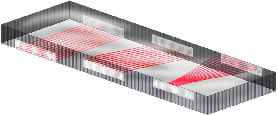
FIGURE 5. Schematic representation of a glass substrate containing waveguides (shown in red) on the bottom surface (left), within the bulk glass (middle), and on the top surface (right).
3.2.1 2D planar ion-exchanged waveguides
Low-loss (<0.1 dB/cm at 1,310 nm) single-mode ion-exchanged waveguides were fabricated on a 150 mm diameter alkali-containing aluminosilicate glass wafer in a pattern that required singulation into individual optical circuits as shown in Figure 1. Since the waveguides are formed a few microns beneath the surface, the optical-quality region only needs to be in that location as shown in Figure 5 (right). An example of a laser singulated optical circuit with an optical-quality region around 5 ion-exchanged waveguides is shown in the end-view optical micrograph of Figure 6A. This region was formed by a single pass of a Bessel beam with a focal offset position lowered such that the modification threshold of the glass started 125 μm below the surface, thereby providing enough space for a single mode optical fiber to couple light into the waveguide. The top-view optical micrograph in Figure 6B shows the laser singulated glass substrate after separation. The red arrow indicates the start of the 6.5 mm long waveguide region where the laser perforations transition from extending through the entire substrate to starting 125 μm below the surface. The ion-exchanged waveguides are not visible with the present lighting, however, the lithographically defined alignment lines (discussed in Section 4.2) are apparent.
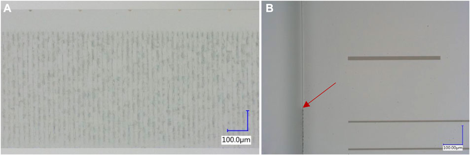
FIGURE 6. (A) End-view and (B) top-view optical micrographs of a laser cut optical circuit with an optical-quality region around ion-exchanged waveguides (dark spots on the top surface in (A)). The red arrow indicates the start of the waveguide region where the laser modifications start 125 μm below the surface.
Figure 7 shows an end-view scanning electron micrograph (SEM) of a laser cut glass substrate with an optical-quality region realized by the absence of laser modifications, similar to the optical micrograph in Figure 6A. This mirror-like finish is desirable for low-loss fiber-to-chip coupling. The inset image confirms that the optical-quality surface has no chipping or other fracture features.
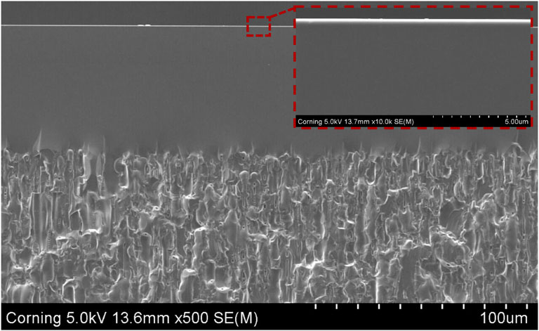
FIGURE 7. End-view SEM micrograph of a laser cut glass substrate with an optical-quality region left near the surface. Inset, a higher magnification image of the region shown in the red square.
To confirm that the mirror-like optical regions would indeed be suitable for low-loss optical coupling, a glass substrate with 12 ion-exchanged waveguides was laser cut leaving an optical-quality region around the waveguides as shown in Figure 6A. The fiber-to-fiber insertion loss (at 1,310 nm wavelength) of the 15 mm long ion-exchanged waveguides was measured after laser singulation with the resulting optical-quality end-facet and again after subsequent optical polishing using traditional methods. The data plotted in Figure 8 reveals on average a difference of 0.04 dB between the two measurements, which is within the experimental error of the measurement. Therefore, the optical-quality end-facets obtained from the laser singulation method can be considered equivalent to those obtained by optical polishing for the purpose of low-loss optical fiber-to-chip coupling.
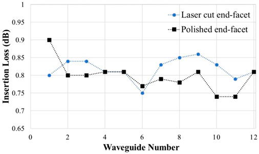
FIGURE 8. Plot showing the insertion loss (at 1,310 nm wavelength) for 12 ion-exchanged waveguides after laser singulation with optical-quality end-facets (blue circles) and again after subsequent polishing (black squares).
3.2.2 Ultrafast laser written 3D optical waveguides
To meet the increasing data center bandwidth demands, the next-generation transceiver modules will need to continue to increase their optical fiber count. Simply increasing the dimensions of these photonic circuits to accommodate more fibers is not a scalable solution as it would increase the overall costs and optical waveguide propagation losses. Increasing the density of optical fibers is the path towards scalability. This has motived the use of reduced cladding (e.g., to 80 μm) and coating (e.g., to 125 μm) diameter fibers to enable higher density optical interconnects (Bickham et al., 2020). Alternative approaches to increasing the fiber-to-chip density, such as using multicore fibers (Djogo et al., 2019) or multi-row fiber connectors, require moving beyond 2D planar waveguide technology to 3D buried waveguides formed in bulk glass by femtosecond laser inscription. However, in many glasses [especially those written in the heat accumulation regime (Eaton et al., 2005)] such as Corning® Eagle XG®, the resulting waveguides taper and can have defects near the end-facets (Figure 9A) due to the focal distortions as the focused laser beam encounters the air-glass boundary at the side edges of the substrate. These distortions increase the waveguide coupling loss and while mitigation approaches using a spatial light modulator to shape the beam to pre-compensate for these focal distortions has been demonstrated (Salter and Booth, 2012), the most common approach is to polish the substrate end-facets post-fabrication. Femtosecond laser written waveguide are also combined with laser modifications tracks that require subsequent chemical etching to define fiber guiding sockets (Djogo et al., 2019) or fiber V-grooves (Psaila, 2019) to improve fiber-to-chip connectivity. This can result in a small section of the optical waveguide near the end-facet to become etched, which leads to a significant coupling loss. Laser singulation can be used instead of end-facet polishing to address the abovementioned challenges efficiently.
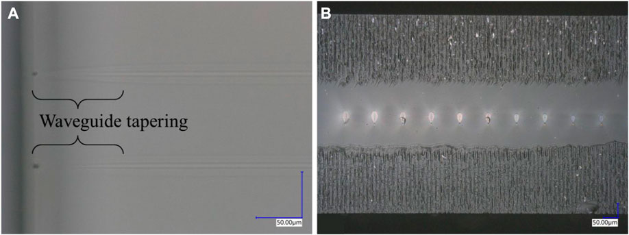
FIGURE 9. (A) Top-view and (B) end-view (post laser cutting) optical micrographs of femtosecond laser written waveguides in Corning® Eagle XG® glass.
As discussed in Section 3.2, the Bessel beam laser cutting technique used to singulate glass substrates with optical-quality end-facets can be applied to waveguides in the bulk glass as shown in Figure 9B. In this example, pulses from 1,030 nm fs (300 fs) laser set at 500 kHz repetition rate were focused through a 40× (0.55 NA) lens to write 50 mm long waveguides 250 µm below surface of a Corning® Eagle XG® glass substrate at a scan speed of 10 mm/s. Note that these waveguides were not optimized and only used to demonstrate the laser singulation with optical-quality regions around them. The controlled placement of the laser modifications above and below the waveguides was achieved by two passes with adjusted focal position offsets.
4 Fiber-to-chip connectivity using passive alignment
In datacenters, next generations switches will require advanced fiber-to-chip connectivity and novel packaging concepts to meet the cost per capacity targets which are increasingly driven by the photonic integration, packaging, and assembly costs. This challenge can be met by enabling the (MPO) interface at the edge of integrated glass waveguide substrates. A major cost saving can also be realized by replacing the complex active alignment process for fiber-to-chip coupling. In this section, a passive alignment technique is demonstrated by accurately forming laser-ablated alignment trenches on the glass substrate that can hold the MPO guide-pins in place and thereby enable the connector to be mated.
4.1 Concept and design of trenches
In this work, laser-formed trenches are accurately positioned on the glass waveguide substrates in order to mount the 550 μm diameter guide pins from an MPO-16 connector as shown in Figure 10A. The 5.4 mm long trenches are separated by 5.3 mm, and have a width designed so that when the guide pins rest on the top edges of the trench, the height of fiber connector waveguides align to the ion-exchanged glass waveguide array. In this way, the trench depth profile (Figure 12B) does not need to be uniform or accurately controlled, but rather only needs to be greater than the amount (30 μm) by which the guide pin protrudes into the trench below the glass substrate. Another advantage of this design is that any fabrication error in the designed trench width only results in a vertical misalignment between the fiber connector and ion-exchanged waveguides by approximately one-fourth of that amount. To minimize the lateral misalignment of the connector interface, and hence the coupling loss, the high accuracy placement of the laser-formed trenches was achieved by using automated vision recognition on lithographically defined fiducials from the ion-exchanged diffusion mask layer.
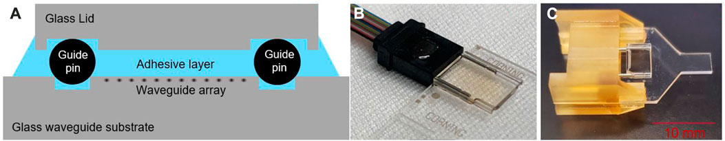
FIGURE 10. (A) End-face view of a fiber-to-chip connector concept to enable connectorization with an (B) MPO-16 ferrule or (C) MPO-16 adapter.
After the trenches were formed, a guide pin was inserted into each trench and a 0.7 mm thick glass lid was bonded on top using an adhesive as illustrated in Figure 10A. The composition of the glass lid was chosen to be the same as the waveguide substrate to ensure a matched coefficient of thermal expansion and thus minimize any thermo-mechanical stress. Once assembled, an MPO-16 ferrule could be easily connected using the guide pins, as shown in Figure 10B, and index matching material applied at the interface. Then, no force is required to push the fibers constantly against the glass waveguide facet. Alternatively, an adapter (Figure 10C) was designed, and precision machined from polyetherimide plastic (ULTEM-1000) to enable physical contact with a standard MPO-16 connector providing a constant mating force with the fiber ferrule against the glass facet by the spring that is part of the MPO-16 connector assembly. An additional wider trench (820 μm; Figure 11A) located to the left of the two guide-pin trenches was formed to align a custom designed MPO adapter, as shown in Figure 10C. The adapter used the standard latching mechanism of the MPO-16 connector which guide the bores of the MPO-16 ferrule onto the guide pins.
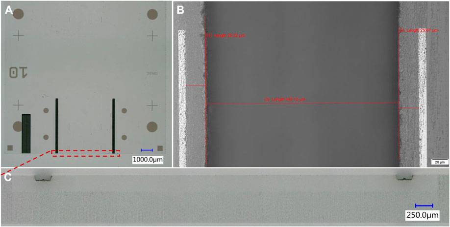
FIGURE 11. Top-view optical micrograph of (A) a 15×15×0.7 mm optical circuit and (B) a magnified section of the laser ablated trench. (C) An end-view optical micrograph of the connector interface region (red dashed rectangle in (A)) showing the laser ablated trenches centered around 12 ion-exchanged waveguides.
4.2 Ultrafast laser-ablated trenches in glass waveguide substrates
After laser singulation, but prior to the actual separation step, laser ablated trenches in which to mount the MPO-16 guide pins were formed. This ensured any ablation debris (minimal with picosecond pulses) remains on top of the wafer, can be easily cleaned, and does not contaminate the end-facets where coupling to optical fibers occurs. To form the laser ablated trenches, pulses from a 532 nm ps (∼10 ps) laser set at 400 kHz repetition rate were routed through a galvanometer laser scanner and focused through an F-Thetha lens (f = 167 mm). The laser power, scan speed, and number of laser passes were optimized to yield the desired trench width and depth (>30 μm) without micro-cracks and/or thermal damage. Once optimized, a study of 16 samples revealed that the standard deviation for trench width and positional accuracy were ±1.2 μm and ±0.4 μm, respectively. These trenches are seen in the top-view image of Figures 11A and a section of one of the laser-formed trenches centered between the two lithographically defined alignment lines is shown with higher magnification in Figure 11B. A 3D image of a section of a trench created using the scanning feature from a digital microscope (Keyence VHX-6000) is shown in Figure 12B and confirms that the depth of the trench is greater than the required 30 μm. This ensures that the guide-pins sit at the desired height as defined by the width of the trenches. The high positional accuracy in the placement of the trenches was achieved by executing a three-point alignment routine that used the center location of three circular fiducials that were extracted by in situ imaging and fitting algorithms. After all the trenches were formed, the wafer was separated into individual optical circuits revealing the optical-quality end-facets that extend beyond the 12 ion-exchanged waveguides to the entire 6.5 mm connector width as shown in Figure 11C.
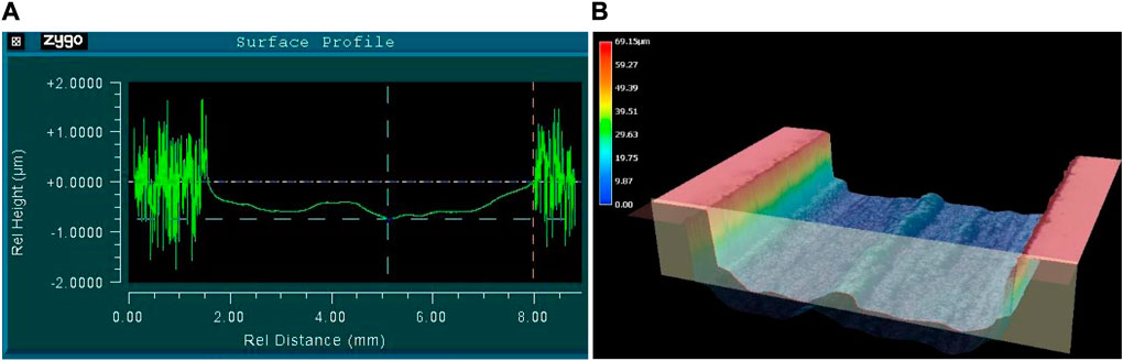
FIGURE 12. (A) Optical profilometer data of the laser cut glass end-facet shown in Figure 11C. (B) 3D profile from a section of the laser-formed trench in Figure 11B.
To assess the flatness along the 6.5 mm long optical-quality region along the end-facet (Figure 11C), an optical profilometer was used to measure the surface profile. Data along a horizontal line extending across the entire optical-quality region, (Figure 12A), reveals that the surface remains flat to within 1 μm, which enables the low-loss coupling to an array of fibers. The higher relative height changes on either side of the optical-quality region are the areas with laser modifications.
To quantify the losses due to the passive alignment technique, the insertion loss of the twelve, 15 mm long ion-exchanged waveguides was first measured using active alignment with single-mode optical fiber on both the input and output sides yielding on average, an insertion loss of 0.82 dB. Next, an MPO-16 adapter (Figure 10C) was assembled and mated with an MPO-16 connector. The applied spring force of 7.5 N provided a constant mating force of the fiber ferrule against the glass waveguide end-face on the input side. An insertion loss of 1.01 ± 0.27 dB was measured after four mating cycles, which after subtracting the baseline insertion loss of 0.82 dB yields on average a misalignment loss of 0.19 dB compared to using active alignment.
5 Conclusion
Glass substrates present many advantages for applications in co-packaged optics where low-loss, high-fiber count connector interfaces are required. In this work, the multi-fiber push-on (MPO) interface was enabled at the edge of integrated glass waveguide substrates providing the opportunity for muti-fiber connectivity using edge coupling. This approach has the additional benefit of leveraging the existing fiber connector eco-system including the ferrule fabrication, fiber assembly, and optical fiber end-face polishing and characterization. Low-loss (<0.1 dB/cm at 1,310 nm wavelength) single-mode optical waveguides were integrated in glass wafers by a silver-ion exchange process and singulated into individual optical circuits by a high-speed ultrafast laser cutting technology. By controlling the gating of the laser pulses as well as the focused laser beam offset, laser modifications could be avoided around the waveguide regions located near the surface or within the bulk glass. The resulting laser singulated end-facets with optical-quality regions were shown to yield the same low-loss coupling as polished end-facets. Ultrafast laser-ablated features were accurately positioned on the glass substrate to enable self-alignment of the MPO connector guide-pins. This passive alignment approach yields on average a 0.19 dB increase in coupling loss compared to using active alignment. The ultrafast laser processing techniques presented in this work address major challenges towards the manufacturing of high-fiber count connectivity solutions for co-packaged optics in next-generation datacenters and high-performance computers.
Data availability statement
The original contributions presented in the study are included in the article; further inquiries can be directed to the corresponding author.
Author contributions
All authors listed have made a substantial, direct, and intellectual contribution to the work and approved it for publication.
Acknowledgments
The authors would like to acknowledge Briar F. Thompson for drafting the illustrations in Figures 1, 5.
Conflict of interest
Authors JG and KW were employed by the company Corning Incorporated, Authors LB and CT were employed by the company Corning Research & Development Corporation, and Author JM was employed by Corning Optical Communications GmbH & Co KG. Some of the work contained in the manuscript relates to a granted patent US11054574B2 Methods of singulating optical waveguide sheets to form optical waveguide substrates.
Publisher’s note
All claims expressed in this article are solely those of the authors and do not necessarily represent those of their affiliated organizations, or those of the publisher, the editors and the reviewers. Any product that may be evaluated in this article, or claim that may be made by its manufacturer, is not guaranteed or endorsed by the publisher.
This manuscript was transferred from Walter De Gruyter GmbH to Frontiers Media SA. The peer review for this paper was conducted in full by Walter De Gruyter GmbH. In accordance with their peer review, editor names and reviewer names have not been published. For any queries regarding the peer review of this manuscript, please contact YWR2YW5jZWRvcHRpY3MuZWRpdG9yaWFsLm9mZmljZUBmcm9udGllcnNpbi5vcmc=.
References
Ashkenasi, D., Kaszemeikat, T., Mueller, N., Lemke, A., and Eichler, H. J. (2012). “Machining of glass and quartz using nanosecond and picosecond laser pulses,” in Proc. SPIE 8243, laser applications in microelectronic and optoelectronic manufacturing (LAMOM) (San Francisco, California, United States: SPIE).
Baghsiahi, H., Wang, K., Kandulski, W., Pitwon, R. C., and Selviah, D. R. (2013). Optical waveguide end facet roughness and optical coupling loss. J. Light. Technol. 31 (16), 2659–2668. doi:10.1109/jlt.2013.2271952
Baltrukonis, J., Ulcinas, O., Gotovski, P., Orlov, S., and Jukna, V. (2020). “Realization of higher order vector Bessel beams for transparent material processing applications,” in Proceedings volume 11268, laser-based micro- and nanoprocessing XIV (San Franscico, California, United States: SPIE).
Barwicz, T., Taira, Y., Numata, H., Boyer, N., Harel, S., Kamlapurkar, S., et al. (2014). “Assembly of mechanically compliant interfaces between optical fibers and nanophotonic chips,” in IEEE 64th Electronic Components and Technology Conference (ECTC), Orlando, FL, USA, 27-30 May 2014 (IEEE).
Bickham, S. R., Marro, M. A., Derick, J. A., Kuang, W. L., Feng, X., and Hua, Y. (2020). Reduced cladding diameter fibers for high-density optical interconnects. J. Light. Technol. 38 (2), 297–302. doi:10.1109/jlt.2019.2939547
Bondarev, K. T., and Malevannyi, I. V. (1956). Cutting glass by abrasive saws. Glass Ceram. 13, 372–375. doi:10.1007/bf00673452
Brusberg, L., Grenier, J. R., and Kocabaş, S. E. (2022). “Glass interposer for high-density photonic packaging,” in Optical Fiber Communications Conference, San Diego, CA, USA, 06-10 March 2022 (IEEE).
Brusberg, L., Whalley, S., Pitwon, R. C. A., Faridi, F. R., and Schröder, H. (2016). Large optical backplane with embedded graded-index glass waveguides and fiber-flex termination. J. Light. Technol. 34, 2540–2551. doi:10.1109/jlt.2016.2529651
Djogo, G., Li, J., Ho, S., Haque, M., Ertorer, E., Liu, J., et al. (2019). Femtosecond laser additive and subtractive micro-processing: Enabling a high-channel-density silica interposer for multicore fibre to silicon-photonic packaging. Int. J. Extrem. Manuf. 1 (4), 045002. doi:10.1088/2631-7990/ab4d51
Du, K., and Shi, P. (2003). Subsurface precision machining of glass substrates by innovative lasers. Glass Sci. Technol. 76 (2), 95.
Dudutis, J., Pipiras, J., Stonys, R., Daknys, E., Kilikevičius, A., Kasparaitis, A., et al. (2020). In-depth comparison of conventional glass cutting technologies with laser-based methods by volumetric scribing using Bessel beam and rear-side machining. Opt. Express 28 (21), 32133–32151. doi:10.1364/oe.402567
Dudutis, J., Stonys, R., Račiukaitis, G., and Gečys, P. (2018). Bessel beam asymmetry control for glass dicing applications. Procedia CIRP 74, 333–338. doi:10.1016/j.procir.2018.08.127
Eaton, S. M., Zhang, H., Herman, P. R., Yoshino, F., Shah, L., Bovatsek, J., et al. (2005). Heat accumulation effects in femtosecond laser-written waveguides with variable repetition rate. Opt. Express 13 (12), 4708–4716. doi:10.1364/opex.13.004708
Flamm, D., Bergner, K., Grossmann, D., Hellstern, J., Kleiner, J., Jenne, M., et al. (2017). “Higher-order Bessel-like beams for optimized ultrafast processing of transparent materials,” in Conference on Lasers and Electro-Optics Europe & European Quantum Electronics Conference (CLEO/Europe-EQEC), Munich, Germany, 25-29 June 2017 (IEEE).
Grenier, J. R., Brusberg, L., Terwilliger, C. C., and Wieland, K. A. (2022). “Ultrafast laser singulation of optical circuits with optical quality end-facets,” in Frontiers in ultrafast optics: Biomedical, scientific, and industrial applications XXII (San Francisco: SPIE).
Hosseini, S. A., and Herman, P. R. (2017). Method of material processing by laser filamentation. USA Patent 20170028505.
Jacoby, M. (2022). As telecom demands grow, optical fibers will need to level up. Chem. Eng. News 98, 10.
Liu, X., Liang, Z., Wen, G., and Yuan, X. (2019). Waterjet machining and research developments: A review. Int. J. Adv. Manuf. Technol. 102, 1257–1335. doi:10.1007/s00170-018-3094-3
Lumley, R. M. (1969). Controlled separation of brittle materials using a laser. Am. Ceram. Soc. Bull. 48, 850–854.
Mahajan, R., Takenobu, S., Laflamme, S., and Engelmann, S. (2016). “Embedded multi-die interconnect bridge (emib) -- A high density, high bandwidth packaging interconnect,” in IEEE 66th Electronic Components and Technology Conference (ECTC), Las Vegas, NV, USA, 31 May 2016 - 03 June 2016 (IEEE).
Malinauskas, M., Žukauskas, A., Hasegawa, S., Hayasaki, Y., Mizeikis, V., Buividas, R., et al. (2016). Ultrafast laser processing of materials: From science to industry. Light Sci. Appl. 5 (8), e16133. doi:10.1038/lsa.2016.133
Marchetti, R., Lacava, C., Carroll, L., Gradkowski, K., and Minzioni, P. (2019). Coupling strategies for silicon photonics integrated chips [Invited]. Phot. Res. 7 (2), 201–239. doi:10.1364/prj.7.000201
Minkenberg, C., Krishnaswamy, R., Zilkie, A., and Nelson, D. (2021). Co-packaged datacenter optics: Opportunities and challenges. IET Optoelectron. 15 (2), 77–91. doi:10.1049/ote2.12020
Ndip, I., Töpper, M., Löbbicke, K., Öz, A., Guttowski, S., Reichl, H., et al. (2012). Characterization of interconnects and RF components on glass interposers. Int. Symposium Microelectron. 2012, 000770–000780. doi:10.4071/isom-2012-wp13
Nisar, S., Li, L., and Sheikh, M. A. (2013). Laser glass cutting techniques—a review. J. Laser Appl. 25 (4), 42010. doi:10.2351/1.4807895
Nisar, S., Sheikh, M. A., Li, L., and Safdar, S. (2009). Effect of thermal stresses on chip-free diode laser cutting of glass. Opt. Laser Technol. 41 (3), 318–327. doi:10.1016/j.optlastec.2008.05.025
Psaila, N. (2019). “3D laser direct writing for advanced photonic integration,” in SPIE photonics west, optical interconnects XIX (San Francisco: SPIE).
Salter, P. S., and Booth, M. J. (2012). Focussing over the edge: Adaptive subsurface laser fabrication up to the sample face. Opt. Express 20 (18), 19978–19989. doi:10.1364/oe.20.019978
Schröder, H., Brusberg, L., Erxleben, R., Ndip, I., Töpper, M., Nissen, N. F., et al. (2010). “glassPack — a 3D glass based interposer concept for SiP with integrated optical interconnects,” in 60th Electronic Components and Technology Conference (ECTC), Las Vegas, NV, USA, 01-04 June 2010 (IEEE).
Smirnov, M. I., Spiridonov, Y. A., and Karapetyan, A. R. (2011). Modern sheet-glass cutting technologies. Glass Ceram. 68 (6), 6–10. doi:10.1007/s10717-011-9310-3
Stoian, R., Bhuyan, M. K., Zhang, G., Cheng, G., Meyer, R., and Courvoisier, F. (2018). Ultrafast Bessel beams: Advanced tools for laser materials processing. Adv. Opt. Technol. 7 (3), 165–174. doi:10.1515/aot-2018-0009
Terbrueggen, R. (2020). “From proof of principle to 98.5% yield of a high-speed laser processing tool,” in Proc. SPIE 11267, laser applications in microelectronic and optoelectronic manufacturing (LAMOM) (United States: SPIE).
Keywords: ultrafast laser processing, co-packaged optics, photonic packaging, optical circuits, glass waveguides
Citation: Grenier JR, Brusberg L, Wieland KA, Matthies J and Terwilliger CC (2023) Ultrafast laser processing of glass waveguide substrates for multi-fiber connectivity in co-packaged optics. Adv. Opt. Technol. 12:1244009. doi: 10.3389/aot.2023.1244009
Received: 21 June 2023; Accepted: 27 July 2023;
Published: 30 August 2023.
Copyright © 2023 Grenier, Brusberg, Wieland, Matthies and Terwilliger. This is an open-access article distributed under the terms of the Creative Commons Attribution License (CC BY). The use, distribution or reproduction in other forums is permitted, provided the original author(s) and the copyright owner(s) are credited and that the original publication in this journal is cited, in accordance with accepted academic practice. No use, distribution or reproduction is permitted which does not comply with these terms.
*Correspondence: Jason R. Grenier, Z3JlbmllcmpyQGNvcm5pbmcuY29t