 Sourav De1,2*
 Md. Aftab Baig1
 Bo-Han Qiu1Franz Müller2Hoang-Hiep Le1
 Maximilian Lederer2
 Thomas Kämpfe2
 Tarek Ali2Po-Jung Sung3Chun-Jung Su3Yao-Jen Lee3
 Darsen D. Lu1*
- 1Institute of Microelectronics, National Cheng Kung University, Tainan, Taiwan
- 2Center for Nanotechnology, Fraunhofer IPMS, Dresden, Germany
- 3Taiwan Semiconductor Research Institute, Hsinchu, Taiwan
This work presents 2-bits/cell operation in deeply scaled ferroelectric finFETs (Fe-finFET) with a 1 µs write pulse of maximum ±5 V amplitude and WRITE endurance above 109 cycles. Fe-finFET devices with single and multiple fins have been fabricated on an SOI wafer using a gate first process, with gate lengths down to 70 nm and fin width 20 nm. Extrapolated retention above 10 years also ensures stable inference operation for 10 years without any need for re-training. Statistical modeling of device-to-device and cycle-to-cycle variation is performed based on measured data and applied to neural network simulations using the CIMulator software platform. Stochastic device-to-device variation is mainly compensated during online training and has virtually no impact on training accuracy. On the other hand, stochastic cycle-to-cycle threshold voltage variation up to 400 mV can be tolerated for MNIST handwritten digits recognition. A substantial inference accuracy drop with systematic retention degradation was observed in analog neural networks. However, quaternary neural networks (QNNs) and binary neural networks (BNNs) with Fe-finFETs as synaptic devices demonstrated excellent immunity toward the cumulative impact of stochastic and systematic variations.
Introduction
The advent of convolutional neural networks (Lecun et al., 2015) has made machine learning or neural network–based computation an inevitable choice for solving many complex tasks in recent times. The real-time processing of the enormous amount of data generated from the internet search engines, social networks, and edge devices in health care systems requires massive computing power in conventional von-Neumann computing architecture. The memory-bandwidth bottleneck in von-Neumann computing and the torrent of data generated on the internet every second have reinvigorated the research in brain-inspired computing. Although modern data centers, furnished by high-performance GPU or TPU, perform the data handling and classification task precisely, the power-hungry nature makes them inappropriate for the end-user devices. Artificial neural networks implemented in such a traditional von-Neumann computing system endure severe bottlenecks during the data transfer between segregated memory and processing units. Quintessentially, there are two pathways for implementing the artificial neural network (ANN). The first one is the computer science–based approach of ANN (Fukushima, 1988; Riesenhuber and Poggio, 1999), which fails to imitate the proper brain functions in terms of power consumption and speed of operations. Therefore, a significant interest in the area of emerging non-volatile memory based on non-von-Neumann computing (Chen et al., 2015; Diehl et al., 2015; Gokmen and Vlasov, 2016; Bae et al., 2017; Ambrogio et al., 2018; Chang et al., 2018; Kim H. et al., 2018; Kim J. et al., 2018; Ernoult et al., 2019; Fu et al., 2019) has grown. The pivotal motivation of the present-day research on the neural network is building dedicated hardware modules for implementing low-power, fast-computing units without affecting the recent trend of scaling.
CMOS-compatibility and low process temperature of hafnium zirconium oxide (HZO) makes HZO-based ferroelectric (Fe) finFETs an excellent candidate for logic, memory, and neuromorphic devices. This property can be attributed to its superior endurance and write speed as compared to Flash, significantly higher on-to-off current ratio than MRAM, as well as the negligible impact from random telegraphic noise due to charge-based operation, unlike RRAM. The advantage of HZO over other perovskite ferroelectric materials and Si-doped hafnium oxides (HSO) has been mentioned in previous reports, which involves ease of deposition by the ALD process, scalability to thin film, and lower process temperature (Muller et al., 2012; Jerry et al., 2017; Kim H. et al., 2018; Ali et al., 2019; Ni et al., 2019; Cheema et al., 2020). Recent reports have also shown that low process temperature, superior interface quality, and reducing the numbers of defect sites in HZO improve the endurance of the HZO-based transistors (Dutta et al., 2020; De et al., 2021a; De et al., 2021b; Khakimov et al., 2021). Apart from the device structure, low process temperature and interface properties, the pulse scheme, and bias-technique during the WRITE operation also play an important role in determining the WRITE-endurance limit of the device. However, the pivotal issue lies in the increasing stochasticity with scaling as well as inherent charge-trapping sites that may capture electrons or holes from the channel side (CS) or gate side (GS) (Dunkel et al., 2017; Alam et al., 2019). These effects create serious reliability issues in terms of degradation of endurance (Dunkel et al., 2017) and increased variation during program–erase (WRITE) operation in deeply scaled HZO-based ferroelectric FET (Fe-FET) devices.
Ferroelectricity is a crystal structure–dependent property engendered from the polarization catastrophe (Slater, 1950; Kittel, 1951; Cochran, 1959; Cowley, 1965). The non-centrosymmetric Pca21 orthorhombic phase is responsible for ferroelectricity in HZO. The other phases, cubic or monoclinic symmetry, do not show ferroelectricity. Therefore, it is essential to form the orthorhombic phase in the HZO film to instigate the ferroelectric switching. Usually, hafnium oxide is doped with silicon, aluminum, or zirconium and subjected to thermal annealing under various conditions to stabilize the metastable ferroelectric orthorhombic phase (Frascaroli et al., 2015; Materlik et al., 2018; Park et al., 2019; Sultana et al., 2019). Despite the adoption of these stabilization techniques, atomic-layer-deposited (ALD) HZO films exhibit non-uniform crystal properties. There have been numerous efforts from the scientific community to find the possible solutions to mitigate these non-idealities for improving the performance of ferroelectric FETs. However, the previous studies on the variability of Fe-FETs have primarily focused on large (>1 µm2) and planar MOSFET devices, in which the random distribution of ferroelectric–dielectric domains and trapping are the two primary sources of variation. Figure 1 provides a qualitative overview of Fe-FET’s applicability as an artificial synapse and the scaling trends toward implementing the finFET-based neuromorphic computing platform from planar CMOS technologies.
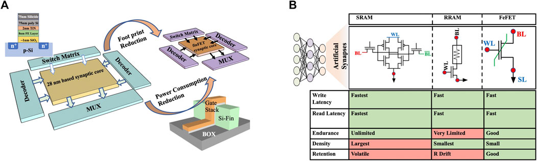
FIGURE 1. (A) Transition from planar FeFET-based neuromorphic circuits to Fe-finFET-based neuromorphic circuit brings several challenges and promises. Although the power consumption and area are reduced, the stochastic variation associated with the scaling will also increase. (B) Qualitative comparison of the critical features of state-of-the-art memory cells highlights the advantage of FeFET as a synaptic device.
The feasibility of 28 nm technology node-based Fe-FETs was successfully demonstrated with the fabrication of such synaptic device in GlobalFoundries facilities (Soliman et al., 2020). Figure 2A illustrates the 28 nm technology node-based FeFET with the schematic and transmission electron microscopic (TEM) image. The binary WRITE operation was conducted by 4.5 and −5 V pulse of 500 ns pulse width. A reset pulse of opposite amplitude preceded each WRITE pulse. Figure 2B shows pulse-driven binary switching capability among sixty devices. Gradual increasing pulse-driven (step size 0.1 V) granular switching capability in a single FeFET cell has been shown in Figure 2C. However, this work focuses on ferroelectric finFETs (Fe-finFETs) fabricated on silicon-on-insulator (SOI) wafers at the Taiwan Semiconductor Research Institute’s nanofabrication facility. The primary geometrical difference between a planar MOSFET and a finFET is that the former is a planar structure, and the latter is a non-planar structure. The process involved in fin formation involves reactive ion etching (RIE) of the bottom electrode (Si-fin), which is not required in planar MOSFETs. We have observed that during RIE, the line edge roughness of the sidewalls of the Si-fin is increased, and the RIE via H-Br plasma creates a Si–Br bond at the interface (Bestwick and Oehrlein, 1990). The primary issues with the degradation in Fe-finFET’s performance are three-fold. First, the random variation of the ferroelectric and dielectric phase in gate-stack was reported by De et al. (2021a) that long duration annealing could mitigate the issues associated with the random distribution of the ferroelectric–dielectric phase in HZO. The second is parasitic charge clouds at the interface and fin line-edge-roughness (LER), which increases the charge-trapping probability and inhibits fast WRITE. Previous reports have shown that surface treatment can alleviate the issues associated with the poor interface quality and reduce the device-to-device variations up to a maximum 10% deviation from the mean value (De et al., 2021a; De et al., 2021b). The final and third one is systematic retention degradation, which directly impacts the inference operation (Baig et al., 2021).
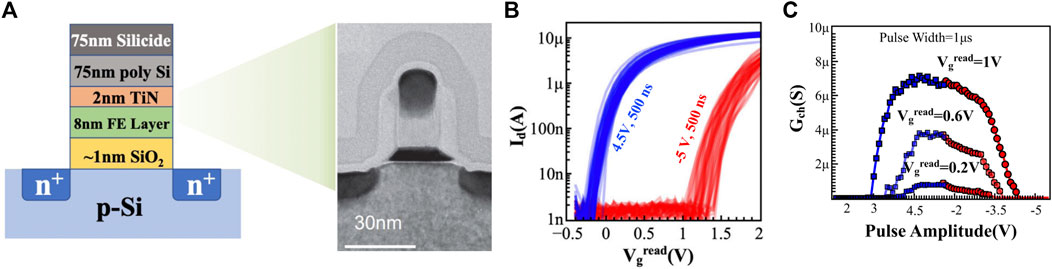
FIGURE 2. (A) Schematic illustration with the transmission electron micrograph of the FeFET cell fabricated in the GlobalFoundries’ 28-nm HKMG facility. (B) Program-–erase operation conducted across sixty test devices using 1 µs pulse of amplitude ±5 V. (C) Analog program–erase operations in a single FeFET cell show the impact of Vgread on the number of different states and linearity (Soliman et al., 2020; Lederer et al., 2021).
This work focuses on evaluating the impact of systematic retention degradation and random device-to-device and cycle-to-cycle variations on the training and inference accuracy of Fe-finFET-based neural networks. In the first part of this article, we describe the fabrication, characterization, and analysis of variability in Fe-finFETs. The second part of this article evaluates the impact of experimentally observed device-to-device and cycle-to-cycle variation on training and inference operation. Neural network simulation is performed using the CIMulator (Le et al., 2020) software platform. Fe-finFETs may also be used for online training, which requires constant updating of weight coefficient (memory write) during training. With endurance up to 109 demonstrated for HZO films (Chung et al., 2018; De et al., 2021b), such application is possible. For inference-only applications, Fe-finFETs form a memory array to perform multiply-and-accumulate (MAC) tasks. It is programmed only one time to store the weight coefficient of the neural network and used for MAC operations by read-only (READ) operations without changing weights (memory write), which necessitates the stable data retention capability. Systematic variations, such as retention degradation, are expected to play an essential role in inference-only applications, whereas cycle-to-cycle variation, physically originating from random telegraphic noise, is expected to play a crucial role in both inference and training applications. Based on our findings, we conclude that the quaternary neural network (QNN) demonstrates higher immunity than the analog neural network toward systematic and random variation.
Materials and Methods
The voltage-dependent partial switching mechanism in HZO-based Fe-finFETs (Trentzsch et al., 2016; Jerry et al., 2017) can be exploited to obtain analog synaptic behavior. However, the infidelity in updating the conductance states of all the devices in the memory array in a reliable manner during the weight update process possesses a fundamental challenge in designing an analog neural network using FeFET devices as a synapse. The following section extends the investigation on such variation in Fe-finFET devices and their applicability as synaptic devices in neural networks’ training and inference operation.
Hf0.5Zr0.5O2-Based Ferroelectric FinFET Fabrication, Characterization, and Modeling
Nanoscale n-type and p-type tri-gate Fe-finFETs were fabricated on an SOI wafer using a gate first self-aligned high-K and metal gate process (De et al., 2021b). The devices under consideration have a gate length (L) of 70 nm and fin width (W) of 20 nm. The fin height (H) for all devices was fixed at 30 nm, and the thickness of the ferroelectric (TFe) layer was 10 nm. Figure 3 schematically illustrates the process flow. During the fabrication process, dry oxidation was performed after fin formation by e-beam lithography. This oxide layer was used as a sacrificial layer to reduce fin line-edge-roughness engendered from lithography and dry-etching process. This oxide layer was removed by diluted hydrogen fluoride (DHF) solution, followed by chemical oxidation via hydrogen peroxide (H2O2) solution to form a relatively thinner interfacial oxide layer of thickness 0.8–1 nm. This process reduces the interfacial trap densities by removing the impurities from the surface of the silicon (Si) fin. The gate stack consisting of HZO and TiN was formed by the atomic layer deposition (ALD) and physical vapor deposition (PVD) method on top of the interfacial layer. Figure 3 also displays the schematic process illustration and transmission electron micrograph (TEM).
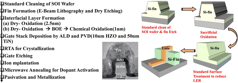
FIGURE 3. Schematic illustration of the process flow along with the TEM image for the front end of line integration of the ferroelectric thin film with finFETs (De et al., 2021a; De et al., 2021b).
The electrical characterization of the devices was carried out by an Agilent B1530A Arbitrary Waveform Generation and Measurement unit. The program (WRITE-1) and erase (WRITE-0) characteristics were analyzed to understand device-to-device and cycle-to-cycle variation in fabricated devices. The devices were subjected to 1-µs-wide pulses with positive or negative amplitudes for characterizing their dynamic behavior, including their response to WRITE operation, multilevel programming behavior, symmetry, and linearity. The characterization of the multi-fin Fe-finFET device was conducted by 1-μs-wide pulses. The low threshold voltage (LVT) state was achieved by applying an +8 V pulse at the gate terminal. On the other hand, a high-voltage state (HVT) was achieved using a pulse of opposite (negative) polarity with similar width and magnitude. To facilitate granular switching and obtain multilevel potentiation and depression characteristics in a single device, we applied a 1-μs-wide pulse of increasing (3–8 V with a step of 0.2 V) and decreasing (−0.8 to −5.4 V with a step of −0.2 V) amplitudes to partially polarize the HZO stack in Fe-FET (Figure 4A).
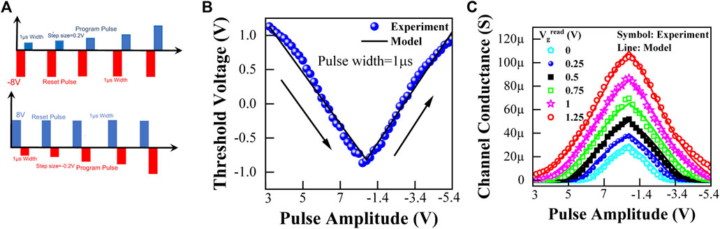
FIGURE 4. (A) LTP–LTD pulse scheme. During the potentiation, the amplitude of the pulse is increased by 0.2 V in each step, and during depression the amplitude is reduced by −0.2 V. A full (±8 V) RESET pulse precedes each potentiation or depression pulse to ensure stable WRITE operation. (B) Threshold voltage modulation curve shows the evolution of threshold voltage after each pulse during gradual potentiation and depression operation. (C) As the threshold voltage changes with program and erase operation, the channel conductance at a fixed gate voltage also varies. Variation of channel conductance is shown here. The number of conductance state depends on the WRITE pulse numbers as well as choice of Vgread.
Although we have observed a ferroelectric domain switching–assisted threshold voltage (Vth) shift upon the application of WRITE pulse of much lower amplitude, the WRITE scheme described in this work is suitable for wafer-scale integration with higher linearity (Lederer et al., 2021). The drain voltage was kept at 0 V during the WRITE operation. Each set (potentiation or depression) pulse was preceded by a reset pulse (±8 V) to drive the conductance back to the starting point. The incrementing WRITE pulse amplitude in each step increments the remnant polarization of the HZO film by a small amount, which inevitably changes the Vth and channel conductance of the Fe-finFETs (Faran and Shilo, 2010; Van Houdt and Roussel, 2018).
The READ of the memory state of the device was accomplished 100 μs after each WRITE pulse. The drain terminal was kept at a constant 100 mV during the READ operation, and a ramp voltage was applied at the gate terminal. The ramp magnitude was varied during the READ operations, similar to Lu et al. (2020), to eradicate the trapping in the HZO film. The conductance was extracted from the Id–Vg curve of potentiation and depression operations at a specific gate voltage. We have used various gate voltages of values 0, 0.25, 0.5, 0.75, 1, and 1.25 V to extract the conductance. Figure 4B shows the highly linear and symmetric threshold voltage modulation traits obtained by partial polarization of the ferroelectric stack in a Fe-finFET with a gate length 70 nm. We have applied positive and gradually increasing pulses for LTP and negative pulses for LTD. Each pulse changes the remnant polarization of the HZO stack, which changes the device’s threshold voltage, thus resulting in a new memory state. We have obtained a maximum of 50 numbers of memory states and a minimum of 26 numbers of memory states for a single device. This variation in available conducting states can be attributed to charge trapping, channel percolation, and nucleation growth domain dynamics (Xiang et al., 2020; Xiang et al., 2021). Figure 4C shows the gradual change in channel conductance during potentiation and depression. The channel conductance is modeled according to one of our previous publications (Lu et al., 2020):
The model is based on the industry-standard BSIM4 model (Dunga et al., 2007). The term “
Although the characterization of a single stand-alone device depicts 26-different conducting states, the device-to-device variation in WRITE operation inhibits 26-level operation in memory arrays. Amid variation, the conductance states start overlapping, and the numbers of available forms start reducing. The root causes for device-to-device variation are the ferroelectric switching process, random distribution of coercive voltage, ferroelectric-dielectric domains, presence of different trapping sites, and surface roughness at the interfaces (De et al., 2021b). The impact of these variations becomes acute, and the number of programming states gets limited to only two when the device is further scaled down. We have obtained bi-directionally programmable 2 bits/cell operation in the fabricated finFET devices with 70 nm gate length and 20 nm fin width. Figure 5A illustrates the pulse scheme used for WRITE operations. Figure 5B demonstrates the 2 bits/cell operation conducted among 12 devices of similar dimensions (L = 70 nm; W = 20 nm). The probability distribution of the channel current, demonstrating the device-to-device variation is shown in Figure 5C. The READ operation was carried out by non-disturbing DC sweep at the gate, and the extraction of the channel current was carried out at the 1 V value of Vgread. Figure 5D demonstrates cycle-to-cycle variation for WRITE operation for four equi-distance current levels. The stability of Vgread is of utmost essential to implement 2 bits/cell operation. Vgread should not alter the programmed state, and it should be high enough to avoid low-frequency noises.
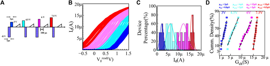
FIGURE 5. (A) Pulse scheme used to obtain 2 bits/cell operation among twelve Fe-finFET devices. (B) READ operation shows 2 bits/cell operation in 12 Fe-finFET devices with a gate length 70 nm and fin width 20 and 10 nm ferroelectric layer. (C) Probability distribution shows four distinct current levels among the devices under consideration. (D) Cycle-to-cycle variation also indicates the presence of four equi-distance current levels in a single cell.
Apart from the multi-bit operation, linearity, and symmetry in WRITE operation, device endurance and retention are two other essential characteristics of neuromorphic applications. Typically, endurance above 107 cycles is required for online training of a fully connected multi-layer perceptron neural network (De et al., 2021b). The endurance characteristics of the fabricated Fe-finFET devices are measured by applying 1-μs-wide pulses of amplitude ±5 V. Figure 6A illustrates the endurance characteristics along with the pulse scheme. The endurance over 109 write cycles in fabricated Fe-finFET devices makes them ideal for online training operations. Once a neural network is successfully trained using online training, the inference operation must be stable. As the online training of neural networks requires high endurance in the synaptic devices, re-training the neural network to compensate for accuracy loss during inference is not a viable option. Therefore, the retention of the synaptic devices plays an essential role in maintaining stable inference accuracy. The conductance drift due to retention degradation was measured by applying a ±5 V pulse of 1 µs width (Figure 6B). The change of Gch for the intermediate states was obtained by linear interpolation. The difference in Gch was captured using a compact model to apply in system-level neural network simulation. We observe that the impact of systematic variations such as retention degradation has a more severe effect on the system-level performance of neural networks than the random variations. Finally, we have benchmarked the performance of the fabricated finFET devices with other emerging non-volatile memories (Table 1).
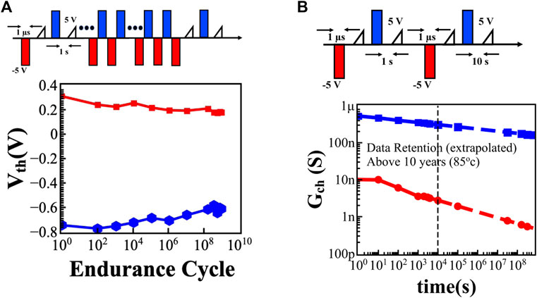
FIGURE 6. (A) Endurance characterization conducted by ±5 V pulse of 1 µs width shows excellent performance up to 109 cycles. Further reduction of amplitude and width of WRITE pulses can improve the WRITE endurance (De et al., 2021b). (B) Endurance and retention characteristics are always counter complimenting. WRITE pulses of lower amplitude and width always engender good endurance characteristics but they result in poor retention. Therefore, optimization of the pulse scheme is necessary to create a balance between endurance and retention characteristics. The retention characteristics, measured at 85°C, show up to 104 s, illustrate excellent extrapolated data retention over 10 years with the same pulse amplitude and width used to measure the endurance.
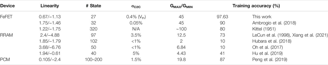
TABLE 1. Device-level benchmarking.
Fe-FinFET as a Synapse in Neuromorphic Applications
To quantify the impact of variations in Fe-finFETs, neuromorphic simulation has been performed. The modeled LTP and LTD characteristics along with the experimentally calibrated device-to-device and cycle-to-cycle variations or the standard deviations (σD2D and σC2C) in Vth distribution have been used to train a Fe-finFET-based multilevel perceptron (MLP)–based neural network with the MNIST data set (Lecun et al., 1998). The layers of the neural network are illustrated in Figure 7A. Figure 7B shows the implementation of ferroelectric devices as a pseudo-crossbar synaptic memory array (Jerry et al., 2017) for the neuromorphic simulation in our CIMulator platform (Le et al., 2020). The CIMulator platform is used to estimate classification accuracy for given device’s characteristics and statistical distribution. Two scenarios are considered. The first scenario is online training, wherein 60,000 MNIST image samples are used to train the hardware neural network, as illustrated in Figure 7. The back-propagation algorithm was adopted for training, with a batch size of 600. In the online training scenario, each device-to-device variation (ΔVth) is fixed at the beginning of training and remains unchanged throughout the training process. For cycle-to-cycle variation, on the other hand, ΔVth changes randomly during READ or WRITE throughout the training process for each device in each cycle. The second scenario is offline training, wherein neural network weight coefficients are pre-trained in software (without considering hardware-related variation). The weights are subsequently written into hardware. Such hardware neural networks will operate differently from software with errors due to device-to-device variation. In this case, there is no chance for the neural network to have its weight adjusted to compensate for hardware-related device-to-device variation.
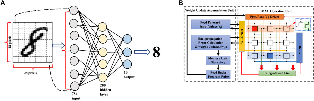
FIGURE 7. (A) Multi-layer perceptron architecture considered during neuromorphic simulation in the CIMulator platform. The network consists of an input layer with 784 nodes, one hidden layer with 200 nodes, and an output layer with 10 nodes. (B) Deploying Fe-FET as an analog synaptic memory array in a simple single layer perceptron.
Results
The online training simulation of Fe-finFET–based synaptic arrays shows that the continuous weight adjustment can avoid the accuracy drop due to device-to-device variations during the training process. While online training is completed, there is minimal accuracy degradation (Figure 8A) due to the sole impact of the device-to-device variation in the WRITE process. Figure 8A highlights that the online training is beneficial toward the robustness of neural networks in the presence of device-to-device variation. For example, for a device with 10% higher intrinsic maximum conductance, the training algorithm automatically adjusts it to have a higher Vth, reducing the conductance by 10% to compensate for the higher intrinsic conductance. This is not the case for offline training. The accuracy drops below 90% when the device-to-device variation exceeds 250 mV.
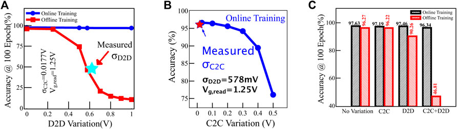
FIGURE 8. (A) Impact of device-to-device variations is significant only for offline-trained neural networks. (B) Impact of cycle-to-cycle variations cannot be compensated by online training. Hardware suggests its effect is negligible. (C) Effect of variations on training accuracy is minimal for hardware-calibrated variability for the online training scenario but is significant for the offline training scenario.
Unfortunately, the online training cannot fully compensate for cycle-to-cycle variation, as this variation source changes from one cycle to another (Figure 8B). The accuracy quickly degrades as cycle-to-cycle becomes larger. A 400 mV cycle-to-cycle variation brings down the accuracy to 90% during the training process. Fortunately, our hardware measurements show that cycle-to-cycle variation is only 17.7 mV in Vth, so accuracy degradation is minimal. Figure 8C shows the cumulative impact of the device-to-device and cycle-to-cycle variation. The degradation in performance in terms of accuracy becomes acute in the offline training scenario. The accuracy was dropped from 97.46 to 90.26% by the device-to-device variation alone. The cumulative effect of the device-to-device and cycle-to-cycle variation deteriorates the recognition accuracy down to 46.81%. Such non-linear behavior is a distinct characteristic of neural networks. When variability is small within a certain threshold, added cycle-to-cycle variation has little impact. On the other hand, once such threshold is reached, the slight randomness of 17.7 mV has a significant effect on degrading neural network classification accuracy.
It is worth noting that in CIMulator, we have adopted the accumulated weight updated method (Hubara et al., 2018) to train the neural network. It is a methodology similar to the Σ-Δ modulation method in communications, which saves the weight residue for each training cycle to compensate for the insufficient weight resolution. It provides good immunity for neural networks with low-weight precision, or low number of states. The downside, however, is the necessity of additional circuits (digital memory) to store the residue portion of the weights, which are not yet written to hardware.
In Figure 9A, we compare the accumulated update mode and the conventional linear update mode, where the weight is rounded to the nearest quantization value with residue discarded. The inference accuracy for linear update mode is near 10% (no recognition capability) until the weights have 6 bits or more (>90% accuracy). On the contrary, the accumulated weight update method requires much lower precision, where 97% inference accuracy can be achieved with only two states or 1 bit. As low Vgread is a pre-requisite for low-power applications of neural networks, the accumulated weight update method is a promising algorithm to train Fe-FET with relaxed requirements for high Vgread (more number of states). Although previous researchers have shown multilevel programming in HZO-based Fe-FETs [40–43], this is the first testament to the number of conducting states on gate voltage for read, Vgread. Therefore, the impact of the Vgread on inference accuracy has been investigated. Figure 9B shows the effect of Vgread for a specific number of bits. Vgread as 1 V, it turns out to be the most optimal solution for all four cases shown in the figure. As discussed in the previous section, this Vgread dependency results from different on–off ratios of channel conductance at different gate voltages during READ operations.
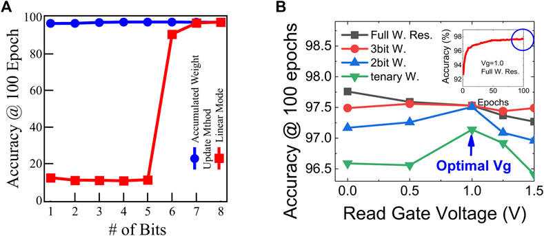
FIGURE 9. (A) Accumulation mode operation requires less number of bits to achieve high accuracy compared to the trivial weight update mechanism. However, this accumulated weight update method requires an extra high precision volatile memory block. (B) Vgread optimization for recognition accuracy.
Finally, we evaluate the cumulative impacts of device variation, retention degradation (assuming Gch drops to 22.6% for HRS and 74.3% for LRS, with intermediate states linearly interpolated), and cycle-to-cycle read variation for inference accuracy (Table 1). Scenario A is the case for the binary neural network (BNN), where all non-ideal-effects-induced accuracy degradation is minimal due to a more significant noise margin. Scenario B is where four-level states are programmed (as in Figure 5), displaying excellent immunity toward such variations. Scenario C is the case where we have considered analog synaptic weights described in Figure 4C. Severe degradation of inference accuracy is observed with retention degradation–induced synaptic weight alteration.
Conclusion
The overall performance of a neuromorphic system is the outcome of the confederated performance of the device, peripheral circuits, network architecture, and algorithm. In this work, we fabricated a nanoscale HZO FeFET device and analyzed the physical reasons for two primary variation sources: 1) paraelectric/ferroelectric phase mixture due to incomplete or insufficient crystallization, which results in the device-to-device variation and 2) random telegraphic noise due to trapping and de-trapping events, which causes the apparent variation from cycle-to-cycle. Experiments are underway to mitigate such variability, especially for small devices. We then translate the observed variability to non-ideality in neural network applications. If online training is possible, 96.34% for MNIST handwritten digits recognition in the presence of variations is achievable. However, offline training may be required due to system constraints, in which case even a moderate device-to-device variation becomes alarming and must be mitigated through further material optimization. We concluded that the impact of experimentally observed variations on system-level accuracy could be negligible by manipulating the neural network algorithm and architecture. Quaternary and binary neural networks both demonstrated excellent immunity toward the cumulative impact of stochastic and systematic variations, whereas the hardware neural network with analog weights shows vulnerability to variation and retention degradation (Table 2).
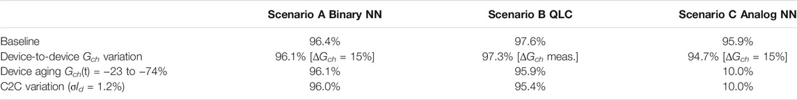
TABLE 2. Cumulative impact of variations on inference accuracy.
Data Availability Statement
The original contributions presented in the study are included in the article/supplementary material; further inquiries can be directed to the corresponding authors.
Author Contributions
The manuscript was written by SD and DL. The primary idea of this research was developed by SD, DL, Y-JL, and TK. Fabrication of the devices and electrical characterization was performed by SD, B-HQ, FM, ML, and TA. MB and H-HL developed the neuromorphic simulation platform and conducted neural network simulation. P-JS, C-JS, and Y-JL developed the Fe-finFET fabrication platform.
Funding
This work was jointly supported by the Ministry of Science and Technology under grant number MOST-108-2634-F-006-008 and MOST-109-2628-E-006-010-MY3 and Lam Research Unlock Ideas 2020.
Conflict of Interest
The authors declare that the research was conducted in the absence of any commercial or financial relationships that could be construed as a potential conflict of interest.
Publisher’s Note
All claims expressed in this article are solely those of the authors and do not necessarily represent those of their affiliated organizations, or those of the publisher, the editors, and the reviewers. Any product that may be evaluated in this article, or claim that may be made by its manufacturer, is not guaranteed or endorsed by the publisher.
Acknowledgments
We are grateful to the Taiwan Semiconductor Research Institute, Fraunhofer IPMS and GlobalFoundries for nanofabrication facilities and services, and National Center for High-Performance Computing, Taiwan, for GPU computing facilities.
References
Alam, Md. N. K., Kaczer, B., Ragnarsson, L.-A., Popovici, M., Rzepa, G., Horiguchi, N., et al. (2019). On the Characterization and Separation of Trapping and Ferroelectric Behavior in HfZrO FET. IEEE J. Electron Devices Soc. 7, 953. doi:10.1109/JEDS.2019.2902953
Ali, T., Polakowski, P., Kuhnel, K., Czernohorsky, M., Kampfe, T., Rudolph, M., et al. (2019). “A Multilevel FeFET Memory Device Based on Laminated HSO and HZO Ferroelectric Layers for High-Density Storage,” in 2019 IEEE International Electron Devices Meeting (IEDM). doi:10.1109/IEDM19573.2019.8993642
Ambrogio, S., Narayanan, P., Tsai, H., Shelby, R. M., Boybat, I., di Nolfo, C., et al. (2018). Equivalent-Accuracy Accelerated Neural-Network Training Using Analogue Memory. Nature 558 (7708), 60–67. doi:10.1038/s41586-018-0180-5
Bae, J.-H., Lim, S., Park, B.-G., and Lee, J.-H. (2017). High-Density and Near-Linear Synaptic Device Based on a Reconfigurable Gated Schottky Diode. IEEE Electron. Device Lett. 38 (8), 1153–1156. doi:10.1109/LED.2017.2713460
Baig, M. A., Hoang-Hiep, L., De, S., Chang, C-W., Hsieh, C-C., Huang, X-S., et al. (2021). Compact Model of Retention Characteristics of Ferroelectric FinFET Synapse with MFIS Gate Stack. Semicond. Sci. Technol. 37 (2), 24001. doi:10.1088/1361-6641/ac3f22
Bestwick, T. D., and Oehrlein, G. S. (1990). Reactive Ion Etching of Silicon Using Bromine Containing Plasmas. J. Vac. Sci. Technol. A: Vac. Surf. Films 8 (3), 6832. doi:10.1116/1.576832
Chang, C.-C., Chen, P.-C., Chou, T., Wang, I.-T., Hudec, B., Chang, C.-C., et al. (2018). Mitigating Asymmetric Nonlinear Weight Update Effects in Hardware Neural Network Based on Analog Resistive Synapse. IEEE J. Emerg. Sel. Top. Circ. Syst. 8 (1), 116–124. doi:10.1109/JETCAS.2017.2771529
Cheema, S. S., Kwon, D., Shanker, N., dos Reis, R., Hsu, S.-L., Xiao, J., et al. (2020). Enhanced Ferroelectricity in Ultrathin Films Grown Directly on Silicon. Nature 580, 7804. doi:10.1038/s41586-020-2208-x
Chen, P.-Y., Lin, B., Wang, I.-T., Hou, T.-H., Ye, J., Vrudhula, S., et al. (2015). “Mitigating Effects of Non-ideal Synaptic Device Characteristics for On-Chip Learning,” in 2015 IEEE/ACM International Conference on Computer-Aided Design (ICCAD). doi:10.1109/ICCAD.2015.7372570
Chung, W., Si, M., and Ye, P. D. (2018). “First Demonstration of Ge Ferroelectric Nanowire FET as Synaptic Device for Online Learning in Neural Network with High Number of Conductance State and Gmax/Gmin,” in 2018 IEEE International Electron Devices Meeting (IEDM), 15.2.1–15.2.4. doi:10.1109/IEDM.2018.8614516
Cochran, W. (1959). Crystal Stability and the Theory of Ferroelectricity. Phys. Rev. Lett. 3 (9), 412. doi:10.1103/PhysRevLett.3.412
Cowley, R. A. (1965). On the Theory of Ferroelectricity and Anharmonic Effects in Crystals. Philos. Mag. 11 (112), 77. doi:10.1080/14786436508230077
De, S., Lu, D. D., Le, H-H., Mazumder, S., Lee, Y-J., Tseng, W-C., et al. (2021a). “Ultra-Low Power Robust 3bit/cell Hf0.5Zr0.5O2 Ferroelectric FinFET with High Endurance for Advanced Computing-In-Memory Technology,” in 2021 Symposium on VLSI Technology, 1–2.
De, S., Qiu, B.-H., Bu, W.-X., Baig, M. A., Sung, P.-J., Su, C.-J., et al. (2021b). Uniform Crystal Formation and Electrical Variability Reduction in Hafnium-Oxide-Based Ferroelectric Memory by Thermal Engineering. ACS Appl. Electron. Mater. 3 (2), 610. doi:10.1021/acsaelm.0c00610
Diehl, P. U., Neil, D., Binas, J., Cook, M., Liu, S.-C., and Pfeiffer, M. (2015). “Fast-classifying, High-Accuracy Spiking Deep Networks through Weight and Threshold Balancing,” in 2015 International Joint Conference on Neural Networks (IJCNN). doi:10.1109/IJCNN.2015.7280696
Dunga, M. V., Lin, C-H., Niknejad, A., and Hu, C. (2007). “BSIM-CMG: A Compact Model for Multi-Gate Transistors,” in Chapter 3 in FinFETs and Other Multi-Gate Transistors. Editor J. P. Colinge (New York, NY: Springer Science Business Media, LLC.), 113–153.
Dunkel, S., Trentzsch, M., Richter, R., Moll, P., Fuchs, C., Gehring, O., et al. (2017). “A FeFET Based Super-low-power Ultra-fast Embedded NVM Technology for 22nm FDSOI and beyond,” in 2017 IEEE International Electron Devices Meeting (IEDM). doi:10.1109/IEDM.2017.8268425
Dutta, S., Ye, H., Chakraborty, W., Luo, Y.-C., San Jose, M., Grisafe, B., et al. (2020). “Monolithic 3D Integration of High Endurance Multi-Bit Ferroelectric FET for Accelerating Compute-In-Memory,” in 2020 IEEE International Electron Devices Meeting (IEDM), 36.4.1–36.4.4. doi:10.1109/IEDM13553.2020.9371974
Ernoult, M., Grollier, J., and Querlioz, D. (2019). Using Memristors for Robust Local Learning of Hardware Restricted Boltzmann Machines. Sci. Rep. 9 (1), 1851. doi:10.1038/s41598-018-38181-3
Faran, E., and Shilo, D. (2010). Twin Motion Faster Than the Speed of Sound. Phys. Rev. Lett. 104 (15). doi:10.1103/PhysRevLett.104.155501
Frascaroli, J., Volpe, F. G., Brivio, S., and Spiga, S. (2015). Effect of Al Doping on the Retention Behavior of HfO2 Resistive Switching Memories. Microelectron. Eng. 147, 43. doi:10.1016/j.mee.2015.04.043
Fu, J., Liao, Z., Gong, N., and Wang, J. (2019). Mitigating Nonlinear Effect of Memristive Synaptic Device for Neuromorphic Computing. IEEE J. Emerg. Sel. Top. Circ. Syst. 9 (2), 377–387. doi:10.1109/JETCAS.2019.2910749
Fukushima, K. (1988). Neocognitron: A Hierarchical Neural Network Capable of Visual Pattern Recognition. Neural Networks 1 (2), 119. doi:10.1016/0893-6080(88)90014-7
Gokmen, T., and Vlasov, Y. (2016). Acceleration of Deep Neural Network Training with Resistive Cross-Point Devices: Design Considerations. Front. Neurosci. 10, 333. doi:10.3389/fnins.2016.00333
Hu, V. P.-H., Lin, H.-H., Zheng, Z.-A., Lin, Z.-T., Lu, Y.-C., Ho, L.-Y., et al. (2019). “Split-gate FeFET (SG-FeFET) with Dynamic Memory Window Modulation for Non-volatile Memory and Neuromorphic Applications,” in Symposium on VLSI Technology, Kyoto, Japan, 134–135. doi:10.23919/VLSIT.2019.8776555
Hubara, I., Courbariaux, M., Soudry, D., El-Yaniv, R., and Bengio, Y. (2018). Quantized Neural Networks: Training Neural Networks with Low Precision Weights and Activations. J. Mach. Learn. Res.
Jerry, M., Chen, P.-Y., Zhang, J., Sharma, P., Ni, K., Yu, S., et al. (2017). “Ferroelectric FET Analog Synapse for Acceleration of Deep Neural Network Training,” in 2017 IEEE International Electron Devices Meeting (IEDM). doi:10.1109/IEDM.2017.8268338
Khakimov, R. R., Chernikova, A. G., Lebedinskii, Y., Koroleva, A. A., and Markeev, A. M. (2021). Influence of the Annealing Temperature and Applied Electric Field on the Reliability of TiN/Hf0.5Zr0.5O2/TiN Capacitors. ACS Appl. Electron. Mater. 3 (10), 4317–4327. doi:10.1021/acsaelm.1c00511
Kim, H., Hwang, S., Park, J., Yun, S., Lee, J.-H., and Park, B.-G. (2018). Spiking Neural Network Using Synaptic Transistors and Neuron Circuits for Pattern Recognition with Noisy Images. IEEE Electron. Device Lett. 39 (4), 630–633. doi:10.1109/LED.2018.2809661
Kim, J., Koo, J., Kim, T., and Kim, J.-J. (2018). Efficient Synapse Memory Structure for Reconfigurable Digital Neuromorphic Hardware. Front. Neurosci. 12, 829. doi:10.3389/fnins.2018.00829
Kittel, C. (1951). Theory of Antiferroelectric Crystals. Phys. Rev. 82 (5), 729. doi:10.1103/PhysRev.82.729
Le, H.-H., Hong, W.-C., Du, J.-W., Lin, T.-H., Hong, Y.-X., Chen, I.-H., et al. (2020). “Ultralow Power Neuromorphic Accelerator for Deep Learning Using Ni/HfO 2/TiN Resistive Random Access Memory,” in 2020 4th IEEE Electron Devices Technology & Manufacturing Conference (EDTM). doi:10.1109/EDTM47692.2020.9117915
LeCun, Y., Bengio, Y., and Hinton, G. (2015). Deep Learning. Nature 521 (7553), 436–444. doi:10.1038/nature14539
LeCun, Y., Bottou, L., Bengio, Y., and Haffner, P. (1998). Gradient-Based Learning Applied to Document Recognition. Proc. IEEE 86 (11), 2278–2324. doi:10.1109/5.726791
Lederer, M., Kämpfe, T., Ali, T., Müller, F., Olivo, R., Hoffmann, R., et al. (2021). Ferroelectric Field Effect Transistors as a Synapse for Neuromorphic Application. IEEE Trans. Electron Devices 68 (5), 2295–2300. doi:10.1109/TED.2021.3068716
Lu, D. D., De, S., Baig, M. A., Qiu, B.-H., and Lee, Y.-J. (2020). Computationally Efficient Compact Model for Ferroelectric Field-Effect Transistors to Simulate the Online Training of Neural Networks. Semicond. Sci. Technol. 35 (9), 95007. doi:10.1088/1361-6641/ab9bed
Materlik, R., Künneth, C., Falkowski, M., Mikolajick, T., and Kersch, A. (2018). Al-, Y-, and La-Doping Effects Favoring Intrinsic and Field Induced Ferroelectricity in HfO2: A First Principles Study. J. Appl. Phys. 123 (16), 1746. doi:10.1063/1.5021746
Muller, J., Boscke, T. S., Schroder, U., Mueller, S., Brauhaus, D., Bottger, U., et al. (2012). Al-, Y-, and La-Doping Effects Favoring Intrinsic and Field Induced Ferroelectricity in HfO2: A First Principles Study. Nano Lett. 12 (8), 4318–4323. doi:10.1021/nl302049k
Ni, K., Chakraborty, W., Smith, J., Grisafe, B., and Datta, S. (2019). “Fundamental Understanding and Control of Device-To-Device Variation in Deeply Scaled Ferroelectric FETs,” in 2019 Symposium on VLSI Technology. doi:10.23919/VLSIT.2019.8776497
Oh, S., Kim, T., Kwak, M., Song, J., Woo, J., Jeon, S., et al. (2017). HfZrOx-Based Ferroelectric Synapse Device with 32 Levels of Conductance States for Neuromorphic Applications. IEEE Electron. Device Lett. 38 (6), 732–735. doi:10.1109/LED.2017.2698083
Park, M. H., Lee, Y. H., and Hwang, C. S. (2019). Understanding Ferroelectric Phase Formation in Doped HfO 2 Thin Films Based on Classical Nucleation Theory. Nanoscale 11 (41), 5786. doi:10.1039/C9NR05768D
Peng, Y., Xiao, W., Han, G., Liu, Y., Wu, J., Wang, K., et al. (2019). Nanocrystal-embedded-insulator (NEI) Ferroelectric Field-Effect Transistor Featuring Low Operating Voltages and Improved Synaptic Behavior. IEEE Electron Devices Lett. 40 (12), 1933–1936. doi:10.1109/LED.2019.2947086
Riesenhuber, M., and Poggio, T. (1999). Hierarchical Models of Object Recognition in Cortex. Nat. Neurosci. 2 (11), 1019–1025. doi:10.1038/14819
Slater, J. C. (1950). The Lorentz Correction in Barium Titanate. Phys. Rev. 78 (6), 748. doi:10.1103/PhysRev.78.748
Soliman, T., Müller, F., Kirchner, T., Hoffmann, T., Ganem, H., Karimov, E., et al. (2020). “Ultra-Low Power Flexible Precision FeFET Based Analog In-Memory Computing,” in 2020 IEEE International Electron Devices Meeting (IEDM), 29.2.1–29.2.4. doi:10.1109/IEDM13553.2020.9372124
Sultana, R., Islam, K., Rakshit, A., Mukherjee, M., and Chakraborty, S. (2019). Effect of Zr Doping and Lattice Oxygen Release on the Resistive Switching Properties of Zr Hf1−O2-Based Metal-Oxide-Semiconductor Devices. Microelectron. Eng. 216, 99. doi:10.1016/j.mee.2019.111099
Trentzsch, M., Flachowsky, S., Richter, R., Paul, J., Reimer, B., Utess, D., et al. (2016). “DecemberA 28nm HKMG Super Low Power Embedded NVM Technology Based on Ferroelectric FETs,” in 2016 IEEE International Electron Devices Meeting (IEDM). doi:10.1109/IEDM.2016.7838397
Van Houdt, J., and Roussel, P. (2018). Physical Model for the Steep Subthreshold Slope in Ferroelectric FETs. IEEE Electron. Device Lett. 39 (6), 877–880. doi:10.1109/LED.2018.2829604
Xiang, Y., Garcia Bardon, M., Kaczer, B., Alam, Md. N. K., Ragnarsson, L. Å., Kaczmarek, K., et al. (2021). Compact Modeling of Multidomain Ferroelectric FETs: Charge Trapping, Channel Percolation, and Nucleation-Growth Domain Dynamics. IEEE Trans. Electron Devices 68 (4), 2107–2115. doi:10.1109/TED.2021.3049761
Xiang, Y., Garcia Bardon, M., Kaczer, B., Alam, Md. N. K., Ragnarsson, L. Å., Groeseneken, G., et al. (2020). “Implication of Channel Percolation in Ferroelectric FETs for Threshold Voltage Shift Modeling,” in 2020 IEEE International Electron Devices Meeting (IEDM), 18.2.1–18.2.4. doi:10.1109/IEDM13553.2020.9371907
Keywords: hafnium oxide, ferroelectric finFET, non-volatile memory, variation, neural networks
Citation: De S, Baig MA, Qiu B-H, Müller F, Le H-H, Lederer M, Kämpfe T, Ali T, Sung P-J, Su C-J, Lee Y-J and Lu DD (2022) Random and Systematic Variation in Nanoscale Hf0.5Zr0.5O2 Ferroelectric FinFETs: Physical Origin and Neuromorphic Circuit Implications. Front. Nanotechnol. 3:826232. doi: 10.3389/fnano.2021.826232
Received: 30 November 2021; Accepted: 28 December 2021;
Published: 26 January 2022.
Edited by:
Ying-Chen Chen, Northern Arizona University, United StatesReviewed by:
Sumant Sarkar, Northern Arizona University, United StatesJiyong Woo, Kyungpook National University, South Korea
Copyright © 2022 De, Baig, Qiu, Müller, Le, Lederer, Kämpfe, Ali, Sung, Su, Lee and Lu. This is an open-access article distributed under the terms of the Creative Commons Attribution License (CC BY). The use, distribution or reproduction in other forums is permitted, provided the original author(s) and the copyright owner(s) are credited and that the original publication in this journal is cited, in accordance with accepted academic practice. No use, distribution or reproduction is permitted which does not comply with these terms.
*Correspondence: Sourav De, sourav.de@ipms.fraunhofer.de; Darsen D. Lu, darsenlu@mail.ncku.edu.tw