 Sai Aditya Raman Kuchibhatla
 Michael J. Leamy
- George W. Woodruff School of Mechanical Engineering, Georgia Institute of Technology, Atlanta, Georgia
In this paper we conceptualize electroacoustic transistors based on topologically protected interface states in a reconfigurable valley-Hall topological insulator. Using piezoelectric media and active shunt circuits, we numerically model the spatial inversion symmetry breaking in a unit cell to produce topological bandgaps. These gaps are known to host robust modes for wave propagation along an interface. We use two such modes to design a transistor where the wave propagation in one topological channel switches on or off a second topological channel between a source and receiver elsewhere in the structure. Multiple such transistors may be combined to develop logic gates. Further, we develop and simulate the behavior of an electronic circuit which enables the transistor action. Our design opens a pathway to novel wave-based devices which may find applications in structure-based computing, as hybrid multiplexers in communication devices, and as structural switches or embedded sensors in robotics and internet of things.
1 Introduction
Topological acoustics has attracted attention in recent years owing to the robustness of edge and interface states exhibiting scattering-free wave propagation. First identified as electronic states in condensed matter (Hasan and Kane, 2010; Qi and Zhang, 2011; Lu et al., 2014), such phenomena have now been established in photonic (Haldane and Raghu, 2008; Raghu and Haldane, 2008; Khanikaev et al., 2013), electromagnetic (microwave frequencies) (Wang et al., 2009; Poo et al., 2011) and acoustic media (Fleury et al., 2014; Yang et al., 2015; He et al., 2016). Topological modes found in acoustics are analogs of quantum effects such as the quantum Hall effect (QHE) (Von Klitzing, 1986), quantum spin-Hall effect (QSHE) (Kane and Mele, 2005), or quantum valley-Hall effect (QVHE) (Mak et al., 2014). While the quantum Hall effect requires breaking time reversal symmetry (TRS) in the system, the other two only require spatial inversion symmetry (SIS) to be broken. The robustness associated with the simpler SIS breaking is lower than with TRS breaking (Noh et al., 2018). However, the waveguiding offered by such topological insulators is still superior to conventional waveguides (Mousavi et al., 2015). Amongst the three, QVHE-analogs are the simplest to achieve as they do not require external bias, like QHE-analogs, or strong coupling of modes, like QSHE-analogs. QVHE was first predicted in graphene (Rycerz et al., 2007; Xiao et al., 2007; Yao et al., 2008; Zhang et al., 2011) and subsequently observed in solid-state devices (Gorbachev et al., 2014; Mak et al., 2014; Sui et al., 2015).
A valley-Hall topological insulator (VHTI) is typically designed from a hexagonal unit cell with SIS (or closely-related mirror symmetry (Lu et al., 2017)) known to possess Dirac cones (Ochiai and Onoda, 2009; Mei et al., 2012; Li et al., 2014)) in its band structure. The inversion symmetry is broken to open a topological bandgap at the vertex of the Dirac cone. At frequencies within the gap, topologically protected waves propagate along an interface of two mediums composed of distinct, mirrored SIS-broken unit cells on either side. VHTIs have been demonstrated using photonic (Ma and Shvets, 2016; Dong et al., 2017) and acoustic periodic media (Zhang et al., 2018; Kliewer et al., 2021; Qu et al., 2021; Wang et al., 2021). Particularly in elastic systems, VHTIs have been demonstrated by breaking mirror symmetry through thickness variations (Ma et al., 2019), strain field tuning (Liu and Semperlotti, 2018), arrays of resonators (Pal and Ruzzene, 2017), arrangement of localized masses (Vila et al., 2017), and other scatterers (Darabi and Leamy, 2019; Gao et al., 2021).
Topological insulators are attractive candidates for acoustic logic devices as they offer the advantage of nearly scattering-free (lossless) wave propagation through topological channels, which may be scaled using MEMS/NEMS technology. Reconfigurability is a highly desired feature in topological media for supporting the development of wave-based devices offering acoustically-controlled output. In recent literature, researchers have demonstrated a programmable acoustic topological insulator where the sound propagation path is altered by physically moving cylindrical inserts in a hexagonal lattice using solenoids (Xia et al., 2018). Another work proposed topological phononic logic by reconfiguring the geometry of a hexagonal unit cell using ultrasonic heating (Pirie et al., 2022). However, these acoustic topological insulator designs reconfigure on relatively slow time scales. An alternative means to achieving reconfigurability is through changes in material properties. Such reconfigurable topological insulators have been demonstrated using piezoelectric media and active shunt circuits (Darabi et al., 2020a; Darabi et al., 2020b; Darabi et al., 2021). As such, topological waveguiding is achieved near-instantaneously by switching electrical shunts in the system.
In this work, we propose and model an electroacoustic transistor where wave propagation between two locations on the periphery of the device is controlled by an input wave at a peripheral gate location, similar to the operation of a field effect transistor (FET). FETs typically contain three terminals; namely a gate, drain and a source. A voltage at the gate terminal determines the current flow between the drain and source terminals. Similarly, in our proposed device, the presence of a wave input at a gate terminal is used to establish a topological channel between a wave source and a drain (output) located elsewhere in the transistor structure. The amplitude of the input gate wave below or above a set threshold results in OFF or ON states of the output as shown in Figures 1A, B, respectively. We present a general design procedure to develop such electroacoustic transistors and demonstrate, using finite element (FE) simulations, the presence of the required topological interfaces. Further, we develop an electronic circuit which supports the transistor action. The proposed device opens a pathway towards rapid structure-based logic using hybrid electrical-acoustic elements and may find applications in industry 4.0; internet of things (IoT) and robotics as embedded sensors and structural switches; and as multiplexer/demultiplexer elements in next-generation communication devices.
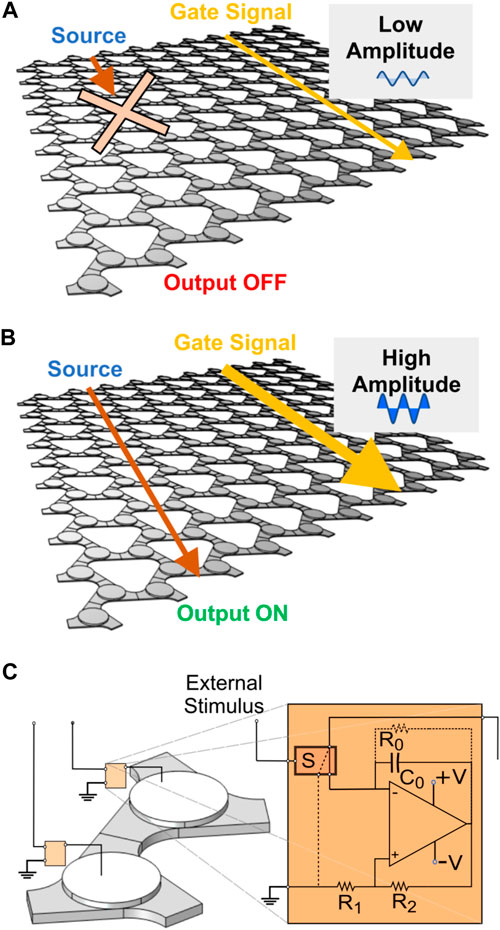
FIGURE 1. Illustration of the proposed transistor in (A) OFF and (B) ON states depicting the absence and presence of an output signal corresponding to low and high amplitude gate signals, respectively. (C) The unit cell of the proposed transistor depicting two piezoelectric disks bonded to an aluminum host and shunted using a negative capacitance circuit via a controllable switch.
2 Electroacoustic unit cell
We begin with the unit cell depicted in Figure 1C. Conceptually, it consists of two piezoelectric disks [e.g., made of lead zirconate titanate (PZT)] bonded to a host material (e.g., aluminum). By using an active shunt circuit, specifically a negative capacitance shunt circuit (Date et al., 2000; Beck et al., 2013; Chen et al., 2014), we can break the spatial inversion symmetry in the unit cell by shunting one piezoelectric disk and short-circuiting the second. The equations governing the piezoelectric media are given as (Erturk and Inman, 2011)
where S denotes the strain, T the stress, D the electric displacement, and E the electric field. The material compliance, electromechanical coupling, and permittivity are denoted by sE, d, and ϵ, respectively. Upon shunting either piezoelectric disk with a negative capacitance circuit, the charge on the PZT for a given strain can be increased or decreased, which results in the variation of the effective elastic modulus via the piezoelectric effect. The elastic modulus, Y, for a simplified case of uniform electric field in the out-of-plane direction, is given as (Date et al., 2000),
where Y0 denotes the short-circuit Young’s modulus of the piezoelectric medium, k31 the electromechanical coupling coefficient, and α = |Cn|/Cp the ratio of negative capacitance, Cn, offered by the shunt circuit, to the inherent capacitance, Cp, of the piezoelectric disk. The negative capacitance shunt circuit can be constructed using an operational amplifier, passive resistances R0, R1 and R2, and capacitance C0, as shown in the circuit depicted in Figure 1C. In this scheme, the circuitry offers a negative capacitance Cn = −C0R2/R1 and can be used to reduce the elastic modulus of the piezoelectric disk. A relay S can be used to switch between shorted and shunted states of the piezoelectric disk. This gives an electrical handle on the unit cell symmetry. Alternatively, the relay could be used to turn on or off the operational amplifier power supply as used in Ref. (Darabi et al., 2021). This would reduce the number of relays used. However, the powered off condition of the supply would result in an open or nearly open circuit configuration of the piezoelectric disk depending on the electrical impedance of the powered-off operational amplifier and passive components. We consider typical values of Y0 = 74 GPa, k31 = 0.37 and Cp = 3.5 nF (e.g., Steminc part # SMD15T09S411) for the PZT disk in the unit cell. A value of α close to 1 results in a large deviation from short-circuit elastic modulus of the PZT. However, practical implementation of such a shunt circuit is prone to instabilities. We consider α = 1.2 to keep the circuit sufficiently away from an electrical instability (Marconi et al., 2020). Using Eq. 2, the shunted PZT modulus obtained with α = 1.2 is Y = 44 GPa. The required Cn = −5.6 nF can be constructed with any combination of the passive components of the NC circuits. For instance, C0 = 1.6 nF, R1 = 1 kΩ and R2 = 3.5 kΩ can be used for this purpose. Typically, a high value for R0 (∼ 1 MΩ) is used to keep the shunt circuit stable at high frequencies. Using the elastic modulus for the shorted and shunted PZTs, the unit cell (and the transistor) can be studied by solving the governing equation for elastic waves (Graff, 2012) with appropriate boundary conditions,
where U denotes the displacement field in the domain. E and ν represent the elastic modulus and Poisson’s ratio of the constitutive material model in various regions of the wave propagation domain. Specifically, E = Y(Y0) for the shunted (short-circuited) PZT disk and E = 69 GPa for the aluminum host domain. Poisson’s ratio of 0.31 and 0.33 are used for PZT and aluminum, respectively. To obtain large asymmetry in the unit cell, we maximize the region in the host geometry bonded to PZT disks. The area of the host not bonded to the PZT disks can be further altered to enhance bandgaps or shift the frequency of the Dirac cones, thus providing a handle on the operating frequency of the transistor. We formulate an eigenvalue problem by applying Bloch boundary condition to a single cell (Phani et al., 2006). Using a commercial FE package (Multiphysics®C. v. 6.0, 2022), we solve the eigenvalue problem and compute the band structure of the unit cell.
Figure 2A depicts the band structure computed along the irreducible Brillouin zone (IBZ) of the unit cell without (left) and with (right) SIS breaking. Multiple Dirac cones can be identified at the K point in the band structure corresponding to the symmetric unit cell, while bandgaps [shaded in Figure 2A] open in the band structure corresponding to the SIS-broken unit cell, as expected. The color represents the flexural polarization of the mode. A value of 1 on the colorbar indicates that the mode is predominantly flexural while a value of 0 indicates longitudinal modes. A complete bandgap of 3 kHz width is found around 48 kHz in the asymmetric unit cell dispersion. Note that the unit cell symmetry can be broken by shunting either the “lower” disk or the “upper” disk while short-circuiting the other. The two resulting asymmetric unit cells are mirror images of each other and have the same eigenvalues, but are topologically distinct (as described below). For the two asymmetric unit cells, the displacement fields at the K points in the Brillouin zone above and below the gap (marked by K + and K− in Figure 2A, respectively) are depicted in Figure 2B. The mode shapes indicate band inversion and the topological nature of the gap. We further confirm this by computing the Berry curvature and the valley-Chern number given by,
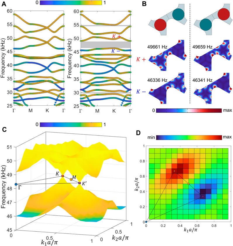
FIGURE 2. (A) Band structure of the unit cell along the IBZ with (left) and without (right) SIS. (B) Displacement field at the K + and K − marked in (A) for mirrored unit cells with broken SIS—red (green) circle indicates shunted (shorted) piezoelectric disk. (C) Dirac cones in the dispersion of the symmetric unit cell at K and K′ points in the Brillouin zone. (D) Numerically computed Berry curvature for unit cell with broken SIS.
and
respectively. Figure 2C shows the Dirac cones in the dispersion (in the reciprocal vector basis) near 48 kHz at the K and K′ points in the Brillouin zone with the colorbar indicating the flexural polarization of the modes. The numerically computed Berry curvature (Blanco de Paz et al., 2020) of the lower band is depicted in Figure 2D. The K and K′ valleys differ in the valley-Chern number by a minus sign as expected. The numerical value (calculated to be ±0.19) deviates from the ideal theoretical value of ±1/2 due to strong SIS breaking (Zhu et al., 2018). For a weaker breaking of inversion symmetry (e.g., shunted PZT modulus of 70 GPa) and thus a smaller bandgap, we obtained a value of ±0.45 for the analogous numerically-computed valley-Chern numbers. With the topological bandgap established, we analyze various possible interfaces to construct an appropriate supercell for the transistor.
3 Topological states for electroacoustic logic
To identify the interface states useful for designing the proposed transistor, we study the eigenmodes of supercells made by repeating the unit cell 10 times in one lattice direction. We apply Bloch boundary condition in the other lattice direction and compute the eigenvalues for the system. The PZT disks neighboring an interface can either be shunted or short-circuited. Further, there can be three different types of interfaces, i.e. armchair, bridge and zigzag (Orazbayev and Fleury, 2019). Here, we consider shorted (type A and B) and shunted (type C and D) interfaces of the zigzag (type B and C) and bridge (type A and D) arrangement such that the interface direction is same as one of the lattice vector directions. The states found in the topological gap are identified as either edge modes or interface modes by visually inspecting their mode shape. Figure 3 depicts the four interfaces that are studied. Also shown are the supercell band structures in the frequency range of interest and the mode shape of the interface state close to a frequency of 49 kHz, marked by a dashed circle in the band structure. The specific operating frequency for the transistor is identified later in the analysis. We refer to the marked state as the ‘first interface mode’ even if it occurs at a higher frequency than other interface modes. In addition to the first interface mode, the supercells with shunted ends (type A and C) or shunted interfaces (type C and D) are observed to host additional modes inside the gap with localization of energy at the respective locations which is similar to the presence of Tamm modes in SSH-like systems (Wang et al., 2018; Chen et al., 2019; Kuchibhatla and Leamy, 2022). We refer to the additional interface state as the “second interface mode”. Figure 4 depicts the out-of-plane displacement field of the two interface modes in the type D interface. The field is normalized to the maxima of the respective eigenmodes for better visualization. The displacement is localized in both the cases with the first interface offering a relatively tighter localization. For constructing the transistor, we look for two interfaces which can be incorporated into a single supercell to enable two distinct states with amplitude localization at the interfaces such that one of them can be switched off by reconfiguring a portion of the supercell. The choice of the type of interface is driven by the availability of distinct topological states over a relatively wide range of frequency within the gap.
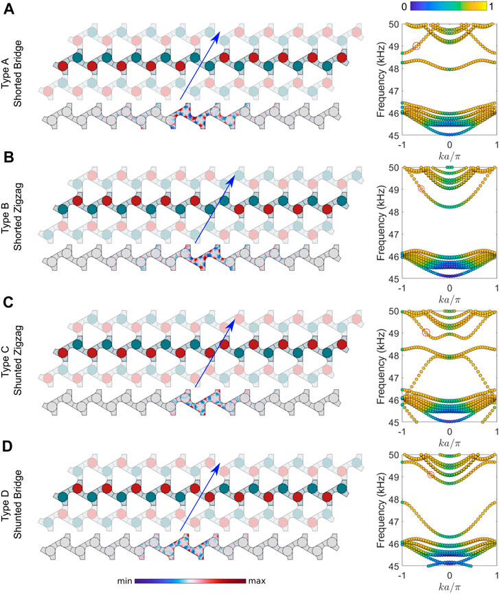
FIGURE 3. Band structures of supercells with two possible cases, neighboring (A,B) shorted and (C,D) shunted PZT disks, of zigzag and bridge type interfaces. The different types of supercells are illustrated with red (green) circles indicating shunted (shorted) PZT disks. The mode shape of the interface state marked by a red dashed circle in the band structure is shown at the bottom of each subfigure.
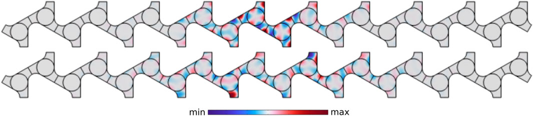
FIGURE 4. Displacement localization in the first (top) and second (bottom) interface mode in the type D interface.
Since either side of the interface must have a differently configured unit cell, it is not possible to combine two of the same type of interfaces into a transistor supercell without causing a defect in periodicity or introducing a third interface (which results in extra localized modes). Instead, we choose two different types of interfaces, A and B, to construct the transistor supercell. The imaginary part of the Bloch wavenumber determines the decay of interface waves into the bulk of the medium. The separation between the two interfaces, or between an interface and the terminated end of the supercell, must be chosen based on the imaginary part of the Bloch wavenumber within the unit cell bandgap. For small values of imaginary Bloch wavenumbers the separation distance needs to be large to ensure the waves originating in the two waveguides, or reflected from the ends of the supercell, do not constructively interfere to result in high amplitude displacements other than at the interfaces. For narrow gaps with small values of imaginary Bloch wavenumber, keeping a large separation distance allows for distinguishable localization at the interfaces. This comes at the cost of an increase in the total size of the transistor structure. Taking advantage of the wide topological gap obtained, we chose 12 unit cells with at least 3 cells between interfaces, or an interface and the end of the supercell. Figures 5A, B depict the proposed transistor supercell in the OFF and ON configurations, along with their band structures indicating the presence of a single interface for the OFF configuration and two interfaces for the ON configuration. Typical mode shapes of the transistor supercell depict the localization of displacement at the two interfaces. One of these interfaces (here type B) can be used at the gate terminal (referred to as the gate interface) for the transistor while the other (type A) serves as the topological channel between the source and drain terminals. The transistor can be switched between the two configurations by changing the shunt status of the piezoelectric disks within the control region in supercells marked in Figure 5. At the chosen operating frequency of 48.8 kHz, we note the presence of the type B interface in both OFF and ON states, while the type A interface only presents in the ON state. As seen in the band structures in Figure 5, there are no other eigenmodes in the system around this frequency and we expect strong localization along these interfaces in a finite structure. As discussed previously, the second interface mode also shows localization at the interface. It is possible to combine, for instance, type C and D interfaces to form a supercell. Using the wider range of frequency offered by the second interface mode, we construct a transistor supercell with 10 unit cells hosting a type D interface at the gate and a type C interface between the source and drain. The supercell is depicted in Figure 6 along with its band structure for OFF and ON configurations. At 47.1 kHz, we find localization in the type D interface in both the OFF and ON states while localization in the type C interface is only present in the ON state (as seen in the modeshapes at the bottom of Figures 6A, B). Again, there are no other eigenmodes in the system around this frequency. These results suggest that the transistor based on the second interface mode is functionally identical to the one based on the first interface mode, albeit at a different operating frequency. We chose to study the transistor behavior using the first interface mode. A transistor based on the second interface mode can be analyzed in the same manner. The transistor action is achieved by switching the control region between ON and OFF states based on an input at the gate using an electrical circuit discussed next.
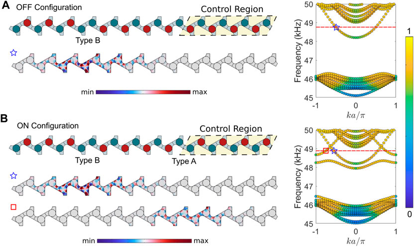
FIGURE 5. (A) OFF and (B) ON states of the transistor supercell constructed using the first interface modes—each subfigure shows the configuration (left), band structure (right) and typical mode shape(s) (bottom) of the interface states. Interface modes for Type B and A are denoted using stars and squares, respectively.
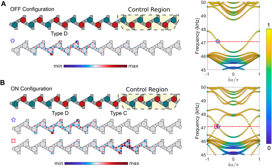
FIGURE 6. (A) OFF and (B) ON states of the transistor supercell constructed using the second interface modes - each subfigure shows the configuration (left), band structure (right) and typical mode shape(s) (bottom) of the interface states. Interface modes for Type D and C are denoted using stars and squares, respectively.
3.1 Switching topological modes
We next describe an electronic module consisting of active feedback circuits using operational amplifiers (OAs) (Sedra and Smith, 1998) which reads the voltage of a PZT disk in the gate interface and outputs an amplified voltage to the relay S in the shunt circuit of Figure 1C. This module is used to control the PZT disks in the control region of the transistor supercell. The module is tuned such that an input wave amplitude above a set threshold generates an output voltage sufficient to trigger the relays, thereby shunting the short-circuited PZTs and short-circuiting the shunted PZTs. Figure 7A depicts the circuit diagram of the electronic module as modeled in Simulink (MATLAB, 2023). The voltage generated across the PZT for small strains is represented by a voltage source. The module amplifies this voltage (using OA1) and rectifies it (using a precision full-wave rectifier implemented with OA2 and OA3) to provide a smooth DC output, which is then amplified by OA4 to supply the trigger voltage. Two different sinusoidal voltages at 48.8 kHz shown in Figures 7B, C, below and above set threshold of 0.1 V (dashed line), are provided as input. The corresponding output of the developed electronic module is shown in Figures 7D, E. The voltage required to trigger a relay (3 V, typical) is marked by a dashed line. Clearly, the module can distinguish a low and high amplitude incoming wave and can trigger the reconfiguring of the control region to switch between the OFF and ON states of the transistor. The threshold values can be conveniently tuned by varying the feedback resistance (marked in Figure 7A as 5R) at the final stage in the electronic module. Next we discuss the predicted response of a finite-sized transistor.
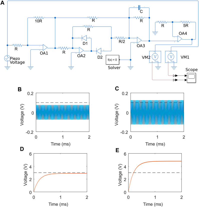
FIGURE 7. (A) Electrical circuit desiged to switch a topological interface. Voltage across a PZT disk (B) below and (C) above a set threshold (dashed line) provided as input to the electrical circuit. (D,E) corresponding output voltage of the circuit.
4 Binary output of the topological transistor
The ability to distinguish low and high amplitude waves allows for bit abstraction using the proposed transistor. With respect to a set threshold, a low (or zero) amplitude wave represents a logical low and a high amplitude wave represents a logical high. We construct a finite transistor structure with 6 repetitions of the supercell in Figure 5. We prescribe a wave input at the gate terminal to mimic an incoming signal. In practice, such an input signal could be generated by an event in the physical surroundings of the transistor, which results in a wave impinging on the domain wall of the device or could be coming from the drain terminal of another transistor. The positions of gate, source and drain are marked using stars and the PZT disk whose voltage is used as input to the electronic module is indicated by a triangle in Figure 8 (left). A continuous wave input independent of the gate is provided at the source. The operating frequency of 48.8 kHz (eigenfrequency of the two interface states identified in the supercell) is used to simulate the harmonic response of the system. Figure 8A depicts the transistor OFF configuration (left) and the displacement field at steady state (right) while the same is depicted in Figure 8B for the ON state. The topological interface between the source and drain has no wave/vibration energy in the OFF state, whereas in the ON state we see a high-amplitude localized standing wave pattern established along the interface. We note that the response in the gate interface is relatively low. This is primarily due to the difference in the wavenumber associated with the interface modes at this frequency which results in different amplitudes of standing waves in the finite structure. The threshold of the electronic module can be tuned to recognize the difference between low and high amplitude inputs specifically in the gate interface. Moreover, each transistor can have a different threshold setting as required by its application.
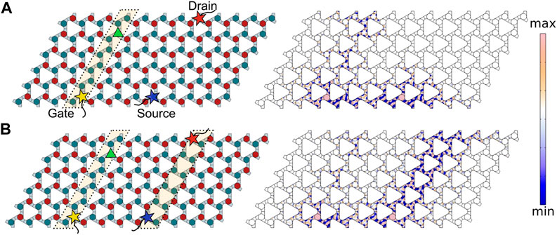
FIGURE 8. The configuration (left) and the displacement field (right) across the finite-sized transistor in the (A) OFF and (B) ON states at an operating frequency of 48.8 kHz. The gate, source and drain terminals of the device are indicated by stars. The triangle indicates the position of the PZT disk in gate interface connected to the electronic module. The topological interfaces in the configurations are highlighted with dashed borderline.
4.1 Boolean operations
The transistor is designed as a monolithic structure and allows us to combine multiple transistors to produce logic gates in a manner similar to conventional FETs. As an example, we present here the design of an AND gate. The designed logic gate is a combination of two transistors. It takes inputs at two gate terminals (IN1 and IN2) to reconfigure the control regions of the two transistors hosted within a single electroacoustic structure. This results in the flow of the wave energy between the source of one transistor and the drain of the second in accordance with the truth table of the logic gate. The reconfigured states corresponding to the different rows of the truth table are shown in Figure 9. A value of 0 in the truth table is equivalent to a low-amplitude wave while a value of 1 indicates a high-amplitude wave at the gate. Since there are no other (edge) modes for wave propagation near the operating frequency the two input waveguides are isolated. Further, as the topological waves are known for minimal scattering at corners, a high amplitude wave in IN1 does not trigger IN2. In a similar manner, logic gates such as OR and NAND can be developed using the proposed transistor by appropriately configuring topological wave paths in tandem.
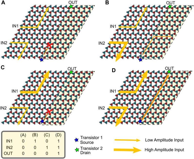
FIGURE 9. Configuration of an AND logic gate for different combinations (A–D) of inputs (IN1 and IN2) listed in the truth table shown at the bottom. 0 (1) in the truth table represents low (high) amplitude wave. Red (green) filled circles represent shunted (shorted) PZT disks. The control region of the logic gate which is reconfigured based on the inputs is marked by dashed line and highlighted.
5 Concluding remarks
In summary, we proposed and numerically verified electroacoustic transistors enabled by reconfigurable interface states in valley-Hall topological insulators. We outlined a design procedure to obtain such interface states in piezoelectric media by using active shunt circuits. We demonstrated through band structure and harmonic response computation that several such states can be leveraged to construct a transistor. Further, we designed and numerically modeled an electronic circuit that enables the transistor action. Such transistors provided two logically distinct states for bit abstraction and can be combined together like conventional electronic transistors to create logic gates. We envision the proposed electroacoustic transistors finding applications as structural switches or embedded sensors for robots and IoT. For example, an autonomous inspection robot deployed in harsh environments may use the proposed transistor on its outer body to distinguish between hard and soft contacts in its path. An impact with an external object (which can be expected to excite a wide frequency spectrum including the operating frequency of the transistor) may be used as the gate signal while the transistor output can be used for course correction or decision making. Further, a similar implementation of the electroacoustic transistor with topological surface acoustic waves may open a pathway for devising robust hybrid devices with applications in telecommunications.
Data availability statement
The original contributions presented in the study are included in the article/Supplementary material, further inquiries can be directed to the corresponding author.
Author contributions
SK and ML conceived the idea. SK performed the numerical simulations and data analysis under the supervision of ML. All authors contributed to the article and approved the submitted version.
Funding
This material is based upon work supported by the National Science Foundation under Grant 1929849. Any opinions, findings, and conclusion or recommendations expressed in this article are those of the authors and do not necessarily reflect the views of the National Science Foundation.
Acknowledgments
SK thanks Dr. Amir Darabi for useful discussions on reconfigurable topological insulators and the computation of valley Chern numbers.
Conflict of interest
The authors declare that the research was conducted in the absence of any commercial or financial relationships that could be construed as a potential conflict of interest.
The author(s) ML declared that they were an editorial board member of Frontiers, at the time of submission. This had no impact on the peer review process and the final decision.
Publisher’s note
All claims expressed in this article are solely those of the authors and do not necessarily represent those of their affiliated organizations, or those of the publisher, the editors and the reviewers. Any product that may be evaluated in this article, or claim that may be made by its manufacturer, is not guaranteed or endorsed by the publisher.
References
Beck, B. S., Cunefare, K. A., and Collet, M. (2013). The power output and efficiency of a negative capacitance shunt for vibration control of a flexural system. Smart Mater. Struct. 22, 065009. doi:10.1088/0964-1726/22/6/065009
Blanco de Paz, M., Devescovi, C., Giedke, G., Saenz, J. J., Vergniory, M. G., Bradlyn, B., et al. (2020). Tutorial: Computing topological invariants in 2d photonic crystals. Adv. Quantum Technol. 3, 1900117. doi:10.1002/qute.201900117
Chen, T., Yu, Y., Song, Y., Yu, D., Ye, H., Xie, J., et al. (2019). Distinguishing the topological zero mode and tamm mode in a microwave waveguide array. Ann. Phys. 531, 1900347. doi:10.1002/andp.201900347
Chen, Y., Huang, G., and Sun, C. (2014). Band gap control in an active elastic metamaterial with negative capacitance piezoelectric shunting. J. Vib. Acoust. 136, 378. doi:10.1115/1.4028378
Darabi, A., Collet, M., and Leamy, M. J. (2020a). Experimental realization of a reconfigurable electroacoustic topological insulator. Proc. Natl. Acad. Sci. 117, 16138–16142. doi:10.1073/pnas.1920549117
Darabi, A., Kliewer, E., and Leamy, M. J. (2021). Reconfigurable acoustic multiplexer/demultiplexer using time division. Appl. Phys. Lett. 119, 113501. doi:10.1063/5.0062735
Darabi, A., and Leamy, M. J. (2019). Reconfigurable topological insulator for elastic waves. J. Acoust. Soc. Am. 146, 773–781. doi:10.1121/1.5114920
Darabi, A., Ni, X., Leamy, M., and Alù, A. (2020b). Reconfigurable floquet elastodynamic topological insulator based on synthetic angular momentum bias. Sci. Adv. 6, eaba8656. doi:10.1126/sciadv.aba8656
Date, M., Kutani, M., and Sakai, S. (2000). Electrically controlled elasticity utilizing piezoelectric coupling. J. Appl. Phys. 87, 863–868. doi:10.1063/1.371954
Dong, J. W., Chen, X. D., Zhu, H., Wang, Y., and Zhang, X. (2017). Valley photonic crystals for control of spin and topology. Nat. Mater. 16, 298–302. doi:10.1038/nmat4807
Erturk, A., and Inman, D. J. (2011). Piezoelectric energy harvesting. Chichester, West Sussex, UK: John Wiley & Sons.
Fleury, R., Sounas, D. L., Sieck, C. F., Haberman, M. R., and Alù, A. (2014). Sound isolation and giant linear nonreciprocity in a compact acoustic circulator. Science 343, 516–519. doi:10.1126/science.1246957
Gao, N., Qu, S., Si, L., Wang, J., and Chen, W. (2021). Broadband topological valley transport of elastic wave in reconfigurable phononic crystal plate. Appl. Phys. Lett. 118, 063502. doi:10.1063/5.0036840
Gorbachev, R., Song, J., Yu, G., Kretinin, A., Withers, F., Cao, Y., et al. (2014). Detecting topological currents in graphene superlattices. Science 346, 448–451. doi:10.1126/science.1254966
Graff, K. F. (2012). Wave motion in elastic solids. Mineola, NY, United States: Dover Publications, Inc.
Haldane, F., and Raghu, S. (2008). Possible realization of directional optical waveguides in photonic crystals with broken time-reversal symmetry. Phys. Rev. Lett. 100, 013904. doi:10.1103/physrevlett.100.013904
Hasan, M. Z., and Kane, C. L. (2010). Colloquium: Topological insulators. Rev. Mod. Phys. 82, 3045–3067. doi:10.1103/revmodphys.82.3045
He, C., Ni, X., Ge, H., Sun, X. C., Chen, Y. B., Lu, M. H., et al. (2016). Acoustic topological insulator and robust one-way sound transport. Nat. Phys. 12, 1124–1129. doi:10.1038/nphys3867
Kane, C. L., and Mele, E. J. (2005). Quantum spin hall effect in graphene. Phys. Rev. Lett. 95, 226801. doi:10.1103/physrevlett.95.226801
Khanikaev, A. B., Mousavi, S. H., Tse, W. K., Kargarian, M., MacDonald, A. H., and Shvets, G. (2013). Photonic topological insulators. Nat. Mater. 12, 233–239. doi:10.1038/nmat3520
Kliewer, E., Darabi, A., and Leamy, M. J. (2021). Additive manufacturing of channeled acoustic topological insulators. J. Acoust. Soc. Am. 150, 2461–2468. doi:10.1121/10.0006452
Kuchibhatla, S. A. R., and Leamy, M. J. (2022). Nonadiabatic shifting of a topological interface in an electroacoustic su-schrieffer-heeger lattice. Phys. Rev. Appl. 18, 054058. doi:10.1103/physrevapplied.18.054058
Li, Y., Wu, Y., and Mei, J. (2014). Double Dirac cones in phononic crystals. Appl. Phys. Lett. 105, 014107. doi:10.1063/1.4890304
Liu, T. W., and Semperlotti, F. (2018). Tunable acoustic valley–hall edge states in reconfigurable phononic elastic waveguides. Phys. Rev. Appl. 9, 014001. doi:10.1103/physrevapplied.9.014001
Lu, J., Qiu, C., Ye, L., Fan, X., Ke, M., Zhang, F., et al. (2017). Observation of topological valley transport of sound in sonic crystals. Nat. Phys. 13, 369–374. doi:10.1038/nphys3999
Lu, L., Joannopoulos, J. D., and Soljačić, M. (2014). Topological photonics. Nat. Photonics 8, 821–829. doi:10.1038/nphoton.2014.248
Ma, J., Sun, K., and Gonella, S. (2019). Valley hall in-plane edge states as building blocks for elastodynamic logic circuits. Phys. Rev. Appl. 12, 044015. doi:10.1103/physrevapplied.12.044015
Ma, T., and Shvets, G. (2016). All-si valley-hall photonic topological insulator. New J. Phys. 18, 025012. doi:10.1088/1367-2630/18/2/025012
Mak, K. F., McGill, K. L., Park, J., and McEuen, P. L. (2014). The valley hall effect in mos2 transistors. Science 344, 1489–1492. doi:10.1126/science.1250140
Marconi, J., Riva, E., Di Ronco, M., Cazzulani, G., Braghin, F., and Ruzzene, M. (2020). Experimental observation of nonreciprocal band gaps in a space-time-modulated beam using a shunted piezoelectric array. Phys. Rev. Appl. 13, 031001. doi:10.1103/physrevapplied.13.031001
Mei, J., Wu, Y., Chan, C. T., and Zhang, Z. Q. (2012). First-principles study of Dirac and Dirac-like cones in phononic and photonic crystals. Phys. Rev. B 86, 035141. doi:10.1103/physrevb.86.035141
Mousavi, S. H., Khanikaev, A. B., and Wang, Z. (2015). Topologically protected elastic waves in phononic metamaterials. Nat. Commun. 6, 8682. doi:10.1038/ncomms9682
Multiphysics®C. v. 6.0 (2022). Comsol. Stockholm, Sweden: COMSOL AB. Avaliable At: www.comsol.com.
Noh, J., Huang, S., Chen, K. P., and Rechtsman, M. C. (2018). Observation of photonic topological valley hall edge states. Phys. Rev. Lett. 120, 063902. doi:10.1103/physrevlett.120.063902
Ochiai, T., and Onoda, M. (2009). Photonic analog of graphene model and its extension: Dirac cone, symmetry, and edge states. Phys. Rev. B 80, 155103. doi:10.1103/physrevb.80.155103
Orazbayev, B., and Fleury, R. (2019). Quantitative robustness analysis of topological edge modes in c6 and valley-hall metamaterial waveguides. Nanophotonics 8, 1433–1441. doi:10.1515/nanoph-2019-0137
Pal, R. K., and Ruzzene, M. (2017). Edge waves in plates with resonators: An elastic analogue of the quantum valley hall effect. New J. Phys. 19, 025001. doi:10.1088/1367-2630/aa56a2
Phani, A. S., Woodhouse, J., and Fleck, N. (2006). Wave propagation in two-dimensional periodic lattices. J. Acoust. Soc. Am. 119, 1995–2005. doi:10.1121/1.2179748
Pirie, H., Sadhuka, S., Wang, J., Andrei, R., and Hoffman, J. E. (2022). Topological phononic logic. Phys. Rev. Lett. 128, 015501. doi:10.1103/physrevlett.128.015501
Poo, Y., Wu, R., Lin, Z., Yang, Y., and Chan, C. (2011). Experimental realization of self-guiding unidirectional electromagnetic edge states. Phys. Rev. Lett. 106, 093903. doi:10.1103/physrevlett.106.093903
Qi, X. L., and Zhang, S. C. (2011). Topological insulators and superconductors. Rev. Mod. Phys. 83, 1057–1110. doi:10.1103/revmodphys.83.1057
Qu, H., Liu, X., and Hu, G. (2021). Topological valley states in sonic crystals with willis coupling. Appl. Phys. Lett. 119, 051903. doi:10.1063/5.0055789
Raghu, S., and Haldane, F. (2008). Analogs of quantum-hall-effect edge states in photonic crystals. Phys. Rev. A 78, 033834. doi:10.1103/physreva.78.033834
Rycerz, A., Tworzydo, J., and Beenakker, C. (2007). Valley filter and valley valve in graphene. Nat. Phys. 3, 172–175. doi:10.1038/nphys547
Sui, M., Chen, G., Ma, L., Shan, W. Y., Tian, D., Watanabe, K., et al. (2015). Gate-tunable topological valley transport in bilayer graphene. Nat. Phys. 11, 1027–1031. doi:10.1038/nphys3485
Vila, J., Pal, R. K., and Ruzzene, M. (2017). Observation of topological valley modes in an elastic hexagonal lattice. Phys. Rev. B 96, 134307. doi:10.1103/physrevb.96.134307
Von Klitzing, K. (1986). The quantized hall effect. Rev. Mod. Phys. 58, 519–531. doi:10.1103/revmodphys.58.519
Wang, L., Cai, W., Bie, M., Zhang, X., and Xu, J. (2018). Zak phase and topological plasmonic tamm states in one-dimensional plasmonic crystals. Opt. express 26, 28963–28975. doi:10.1364/oe.26.028963
Wang, Z., Chong, Y., Joannopoulos, J. D., and Soljačić, M. (2009). Observation of unidirectional backscattering-immune topological electromagnetic states. Nature 461, 772–775. doi:10.1038/nature08293
Wang, Z., Yang, Y., Li, H., Jia, H., Luo, J., Huang, J., et al. (2021). Multichannel topological transport in an acoustic valley hall insulator. Phys. Rev. Appl. 15, 024019. doi:10.1103/physrevapplied.15.024019
Xia, J. P., Jia, D., Sun, H. X., Yuan, S. Q., Ge, Y., Si, Q. R., et al. (2018). Programmable coding acoustic topological insulator. Adv. Mater. 30, 1805002. doi:10.1002/adma.201805002
Xiao, D., Yao, W., and Niu, Q. (2007). Valley-Contrasting physics in graphene: Magnetic moment and topological transport. Phys. Rev. Lett. 99, 236809. doi:10.1103/physrevlett.99.236809
Yang, Z., Gao, F., Shi, X., Lin, X., Gao, Z., Chong, Y., et al. (2015). Topological acoustics. Phys. Rev. Lett. 114, 114301. doi:10.1103/physrevlett.114.114301
Yao, W., Xiao, D., and Niu, Q. (2008). Valley-dependent optoelectronics from inversion symmetry breaking. Phys. Rev. B 77, 235406. doi:10.1103/physrevb.77.235406
Zhang, F., Jung, J., Fiete, G. A., Niu, Q., and MacDonald, A. H. (2011). Spontaneous quantum hall states in chirally stacked few-layer graphene systems. Phys. Rev. Lett. 106, 156801. doi:10.1103/physrevlett.106.156801
Zhang, Z., Tian, Y., Wang, Y., Gao, S., Cheng, Y., Liu, X., et al. (2018). Directional acoustic antennas based on valley-hall topological insulators. Adv. Mater. 30, 1803229. doi:10.1002/adma.201803229
Keywords: wave-based logic, valley-hall effect, elastic topological insulators, reconfigurable metamaterials, piezoelectric devices, shunt circuits
Citation: Kuchibhatla SAR and Leamy MJ (2023) Numerical demonstration of a topologically-protected electroacoustic transistor. Front. Acoust. 1:1251215. doi: 10.3389/facou.2023.1251215
Received: 01 July 2023; Accepted: 24 August 2023;
Published: 19 September 2023.
Edited by:
Bogdan Popa, University of Michigan, United StatesReviewed by:
Serife Tol, University of Michigan, United StatesChristophe Droz, Inria Rennes—Bretagne Atlantique Research Centre, France
Xiuyuan Peng, Apple, Inc, United States
Copyright © 2023 Kuchibhatla and Leamy. This is an open-access article distributed under the terms of the Creative Commons Attribution License (CC BY). The use, distribution or reproduction in other forums is permitted, provided the original author(s) and the copyright owner(s) are credited and that the original publication in this journal is cited, in accordance with accepted academic practice. No use, distribution or reproduction is permitted which does not comply with these terms.
*Correspondence: Michael J. Leamy, bWljaGFlbC5sZWFteUBtZS5nYXRlY2guZWR1