 Zhongming Cao1
 Sorcha Hulme
 Tim D. Veal
 Ian Sandall
- 1Department of Electrical Engineering and Electronics, University of Liverpool, Liverpool, United Kingdom
- 2Department of Physics and Stephenson Institute for Renewable Energy, University of Liverpool, Liverpool, United Kingdom
- 3Department of Physics, University of Warwick, Coventry, United Kingdom
The viability of incorporating Bi and N into GaSb layers to realise photodetectors operating in the mid-infrared has been investigated. The effects of Bi and N on the cut-off wavelength of GaSb metal-semiconductor-metal photodetectors has been evaluated. The spectral responsivity measurements indicate a clear wavelength extension, to 1950 nm (Bi, 2.9%), 1990 nm (Bi, 3.8%), 2080 nm (Bi, 4.5%) and 2190 nm (N, 1.5%) from a reference GaSb device at 1720 nm, with only a relatively modest reduction in the external quantum efficiency (EQE). Comparisons of spectral response characteristics indicate that Bi incorporation reduces the carrier extraction and the impact of this on future device design is considered.
Introduction
The mid-infrared (MIR) spectral range has been widely employed in many sciences and technical fields. Optoelectronic devices working between 2 and 5 μm have great potential in areas such as night vision imaging (Razeghi and Nguyen, 2014), telecommunications (Soibel et al., 2009) and molecular spectroscopy (Haas and Mizaikoff, 2016). Gas sensing with a high resolution is also possible due to many gases, such as CO, CO2, HF and CH4, having strong absorption lines in the MIR domain (Rothman et al., 1992). MIR radiation can also travel through the atmosphere without significant losses, opening potential applications in free-space communications (Karstad et al., 2005). Military vision enhancement, industrial leakage detection and missile tracking are among other important usages of MIR detection.
In order to fulfil the increasing demand, high-performance MIR detectors with high responsivity and low dark current are eagerly pursued. One of the most widely used semiconductor materials for fabricating MIR detectors is Mercury Cadmium Telluride (HgCdTe). The advantages of HgCdTe include the direct band gap, ability to obtain both low and high carrier concentrations (Weiss et al., 2001), and the ability to tune the band gap for detection across a wide part of the infrared region. However, the primary motivation for replacing HgCdTe is the price and the technological disadvantages of material fabrication (Lei et al., 2015), which impair its competitiveness in many applications. Other material such as InGaAs have also been used to target the infrared spectral range due to the similarity of its band structure with that of HgCdTe. Commercial InGaAs photodiodes mainly operate in the wavelength range around 2 μm, some of the InGaAs photodiodes have shown high device performance close to the theoretical limits which can get extended to 2.5 μm, but the performance decreases rapidly beyond this due to large lattice mismatch effects (Jurczak et al., 2017).
Over the past few years, researchers have begun to investigate the dilute GaSb-related alloys such as GaSbBi and GaNSb. Rajpalke et al. developed the growth of GaSbBi with Bi content controlled by varying the temperature (Rajpalke et al., 2013), growth rate (Rajpalke et al., 2014)and Bi flux (Rajpalke et al., 2015). They also used the valence band anti-crossing model and Bi-induced downward shift of the conduction band minimum, implemented using the kp approach, to describe the experimentally observed band gap reduction as a function of Bi (Rajpalke et al., 2013), (Rajpalke et al., 2014), (Rajpalke et al., 2015) and reported temperature-dependence of both photoluminescence and photomodulated reflectance (Kopaczek et al., 2013; Kopaczek et al., 2014). More recently, Das et al. (Das et al., 2019) have investigated the band structure of GaSbBi as functions of Bi mole fraction and along with different symmetry directions of the crystal by using a 14 band kp anti-crossing model. Sharma et al. (Sharma and Dhar, 2019) have applied a two-oscillator model to investigate the temperature dependence of the bandgap energy of GaSbBi. The result indicates that the phonon dispersion co-efficient is reduced with an increase of Bi content in the material. Before GaSbBi research had been established, Buckle et al. developed the growth of GaNSb alloys (Buckle et al., 2005). Band gap reduction of ∼320 meV for 1.52% N incorporation was reported by Veal et al (Veal et al., 2005), and subsequently accounted for by the conduction band anti-crossing model (Jefferson et al., 2006). Their results were broadly confirmed by Wang et al. (Wang et al., 2009) who studied the band structure of dilute nitride GaNSb bulk materials by photoluminescence and optical absorption measurements, demonstrating a bandgap reduction up to 300 meV with increasing nitrogen incorporation. The role of N pair states in determining the evolution of the optical absorption for up to 2.5% N incorporation was subsequently elucidated using the Anderson impurity model (Mudd et al., 2013). In contrast to several studies of thin films, there are only a few reports realizing band structure and optical properties of GaSbBi via a complex optoelectronic device such as quantum well laser diodes (Delorme et al., 2017a; Yue et al., 2018), and no reports to date of any photodetector from these novel alloys. furthermore no optoelectronic device has been reported based on GaNSb. We have previously demonstrated (Cao et al., 2020) the operation of a GaAsBi Metal Semiconductor Metal Photodetector which demonstrated an increased cutoff wavelength compared to a reference GaSb device, indicating the viability of this material system to operate further into the infrared. In this paper, we expand upon this initial proof of concept, to look at a series of GaSbBi layers with increasing Bi content as well as investigating the potential of using GaNSb. The epitaxial growth of a full GaSbBi photodiode structure is complicated, due to the need to grow thick layers with possible strain issues, and the need for doping, additionally the fabrication process will need extensive development of appropriate etching and passivation procedures. As such the work here focuses on utilising thin films of GaSbBi or GaNSb as simple photodetectors to provide the proof of concept devices and begin to study the material quality for future device development. The spectral response characteristics are compared to study the quality of the device and the effect of Bi incorporation on the photo responses.
Experimental Work
The thin film GaSbBi samples were grown by solid-source MBE with a base pressure of 10–10 torr, on GaSb (001) undoped substrates with an initial GaSb 100 nm buffer layer, to a thickness of 350 nm. The Bi incorporations in the GaSbBi epilayers were characterised using Rutherford backscattering (Rajpalke et al., 2015). The Bi concentration in the GaSbBi samples used in this work varied from 2.9 to 4.5%, as listed in Table 1. From our previous work on similar epilayers we would expect the Bi containing films to be p-type with a carrier concentration in the range of 10 × 1018 cm−3 (Segercrantz et al., 2017). The thin film GaNSb used in this work was grown by plasma-assisted MBE semi-insulating GaAs (001) substrates. The N contents of the relaxed films were determined from x-ray diffraction (Segercrantz et al., 2015). The N concentration in the GaNSb sample used in this work is listed in Table 1. A reference GaSb sample with no Bi or N was also grown.
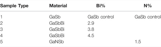
TABLE 1. Content details of GaSb, GaSbBi, and GaNSb samples.
The thin film GaSbBi, GaNSb and GaSb wafers are then fabricated into metal-semiconductor-metal photodetectors (MSM-PDs). The wafers were first cleaved into the size of 1 × 1 cm2 and then cleaned with acetone and isopropyl alcohol for 10 min each. The samples were dried under nitrogen before being patterned with different geometry contacts via a standard photolithography process, using the positive photo-resist Shipley 1813. The interdigital top electrode was patterned, and Al was deposited by thermal evaporation to a thickness of 50 nm. The unwanted Al was lifted off using acetone then the sample was dried under N2. Six different types of geometry with interdigital gaps varying from 20 to 100 μm were compared to study the effect on spectral responses. The details of the different geometries used is listed in Table 2 and Figure 1A. A straight bar and a zig-zag configuration were utilised to enable us to investigate the influence of an increased edge length on the electrodes, while maintaining the same electrode gap spacing. The ratio of metallized to unmetallized area is kept approximately constant for all configurations to ensure that any observed changes are due to device performance and not changes in reflectivity/absorption on the surface of the sample.
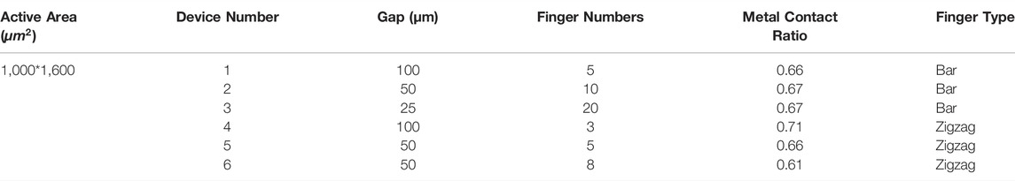
TABLE 2. Detail of different geometry of the interdigital electrode.
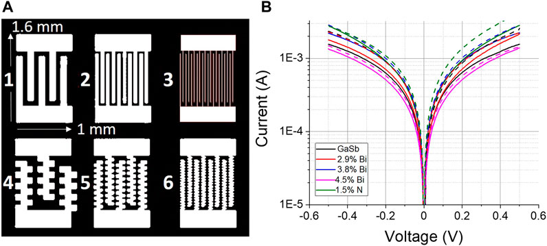
FIGURE 1. (A) Top view geometry of the different interdigital electrode arrangements and (B) current voltage characteristics measured in the dark (solid lines) and light (dashed lines) for devices with geometry 3 electrodes for each sample.
The current voltage responses were measured using a probe station with an Agilent B1500A Semiconductor Device Parameter Analyser, with the samples placed in a Faraday cage, for illuminated measurements a Thorlabs SLS202C broadband source was used. In order to investigate the photo responses upon illumination, the fabricated MSM-PDs sample is placed into a calibrated Horiba iHR320 monochromator system. A Stanford Research SR570 low-noise current pre-amplifier and a Stanford research SR850 DSP lock-in amplifier with an optical chopper are used to recover the photocurrent and minimise the effect of noise. The optical chopper set to a frequency of 330 Hz was placed between the output light source of the monochromator system and the sample. To determine the responsivity and hence external quantum efficiency for the devices the output power from the monochromator is measured and calibrated at each wavelength using a Thorlabs FD05D—InGaAs photodiode.
Result and Discussion
To first verify the devices were working current voltage measurements were performed for each sample in the dark and under broadband IR illumination. The results for the devices from each sample with electrode configuration 3 (straight bar interdigit fingers) in shown in Figure 1B. For all devices a relatively high dark current is observed, but there is a clear increase in the measured current upon illumination.
Figure 2A shows the room temperature spectral responses of the GaSb and GaSbBi MSM-PD devices with the different Bi content (again with electrode configuration 3). The photocurrent spectra have been recorded at a bias voltage of 100 mV, with the incident light focused onto the central region between the electrodes. The spectra have been normalised to the value at the peak photocurrent to aid comparison. Each of the GaSbBi samples demonstrates a clear extension in the cut-off wavelength (defined here as 10% of the maximum intensity) compared to the reference device. As the photocurrent begins to decrease from the peak value the three Bi containg devices show similar behaviour with a constant increase in wavelength compared to the reference device. However once the current has reduced to below 50% of the peak value a clear difference between the three samples is observed with the tail extending further into the red as Bi content is increased. While this spectral shape is a little unusual it is repeatable across multiple devices and a similar effect is seen at other biases, indicating it is real, it is also clearly above the noise floor for the response. The cut-off wavelength has extended from a reference GaSb MSM-PD device at 1720 nm (which has good agreement with literature (Adachi, 1987; Adachi, 1989; Vineis et al., 1998)), to 1950, 1990, and 2080 nm for the GaSbBi MSM-PD devices with 2.9, 3.8 and 4.5% Bi incorporation, respectively. This extended cut-off wavelength is caused by the incorporation of Bi into the active layer of the MSM-PDs, indicating a direct bandgap reduction. The bismuth content of the sample used in this work has been confirmed by Rutherford backscattering experiment in previous work (Rajpalke et al., 2015). Figure 3A, shows the determined cut-off energy as a function of the Bi percentage for the three samples. The resultant linear fit for this data gives a bandgap reduction of 27 ± 3 meV/%Bi. Previous reports for the bandgap reduction, from multiple groups and different measurement techniques have been in the range of 35–40 meV/%Bi at room temperature (Das et al., 2012; Polak et al., 2014; Rajpalke et al., 2014; Samajdar et al., 2015; Delorme et al., 2017b). The calculated energy shift from the GaSbBi valance band to conduction band is 36 meV/%Bi agreeing with these previous studies, indicating that something different is occurring in these devices. Our value of 27 meV agrees much more closely to the energy shift due to spatially indirect transitions between the GaSb valance band and the GaSbBi conduction band (Figure 3B) (Rajpalke et al., 2013; Polak et al., 2014). While we would not expect this to be a dominant transition in this device due to the small interface area between the layers and the low oscillator strength of the transition, the agreement between the values warrants some consideration as a possible explanation. Furthermore such spatially indirect (or type II) transitions have been observed in a number of other III-V based heterostructures operating both as photodetectors and optical emitters (Jiang et al., 2018; Yang, 2020). The absorption coefficient of GaSbBi is relatively low near the bandgap meaning that around 75% of the light incident on the surface reaches the GaSbBi/GaSb interface and as such could contribute to this spatially indirect transition. One possible explanation, for this transition becoming dominant could be due the high density of holes in the GaSbBi coupled with their low mobility, resulting in poor transport of holes and hence low collection efficiency in the GaSbBi layer and hence reducing the probability of the expected direct transition occurring. While the underlying GaSb substrate maintains a fairly high collection efficiency, giving rise to this indirect transition dominating. We can also not exclude the possibility that the value we have measured does correspond to the direct transition, but yielding a different value due to inherent differences between ours and previous work. The previous studies have all utilised passive measurements performed on bare wafer (i.e., photoluminescence, absorption, etc.). Whereas here we are undertaking a more dynamic measurement on a functioning device, introducing a Schottky barrier from the contacts and an external electric field across the device during the absorption process. As such the barrier and electric field may be introducing some band bending. This explanation appears to be less likely as if the change in the expected transition energy was due to the external electric field we would expect the result to change at different biases. However within the experimental error and the range of voltages we were able to apply and still resolve the generated photocurrent we obtain the same value of 27 meV/%Bi.
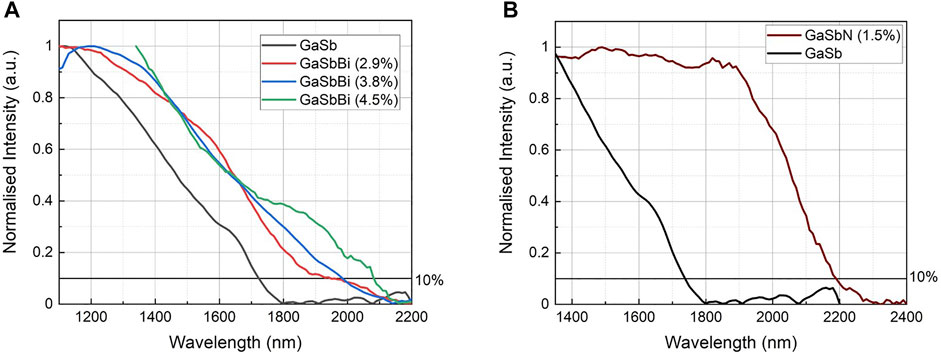
FIGURE 2. Normalised room temperature photocurrent spectra of (A) GaSb and GaSbBi MSM-PDs and (B) GaSb and GaSbN MSM-PDs.
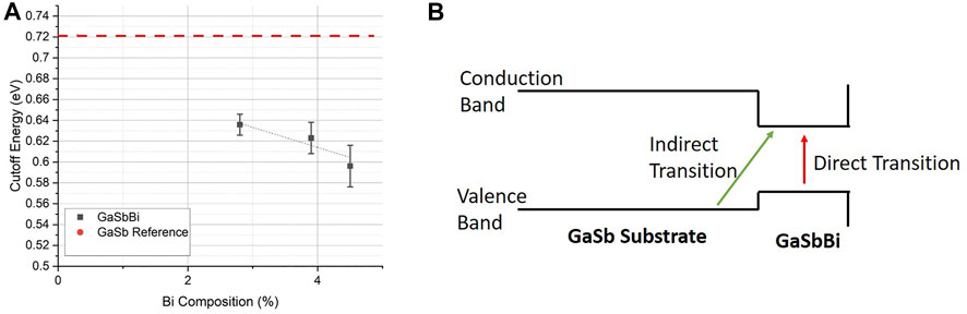
FIGURE 3. (A) Determined cut-off Energy vs Bi concentration at room temperature, the black dotted line gives a linear fit for these values while the red dotted line shows the reference cut-off from the GaSb sample. (B) Band diagram with the direct and indirect optical transitions.
Meanwhile, Figure 2B shows the normalised intensity responses of GaSb and GaNSb MSM-PD device. The GaNSb device with 1.5% N incorporation exhibits a 470 nm wavelength extension compared to the GaSb device, corresponding to an estimated bandgap reduction of 103 meV/%N. However, previous studies on the band structure of GaNSb have calculated the bandgap reduction of N is in a range of 168–300 meV/%N (Veal et al., 2005; Wang et al., 2009; Mudd et al., 2013). The lower than expected bandgap reduction observed in this work could be due to a number of factors, firstly the relatively thin GaNSb layer compared with the thick GaSb substrate, may have resulted in the photo absorption being distorted by reducing the mobility of the carriers leading to a reduced shift of the absorption edge (Wang et al., 2009). Another possibility may be due to a non uniform incorporation of nitrogen during the wafer growth, meaning the part of wafer we have fabricated and tested has a lower than expected Nitrogen composition. To verify this would require a detailed materials characterisation investigation of the wafer using techniques such as RBS, XRD and SIMS, which is beyond the scope of this initial proof of concept device.
However, to the best of our knowledge, this is the first observation of an extended wavelength response in an actual photodetector device based on GaSb alloyed with N or Bi. While the wavelength extension indicates that both Bi and N can indeed be used to extend the operation wavelength of GaSb photodetectors, it does not provide any information regarding any change in efficiency upon Bi and N incorporation.
Figure 4A illustrate the calibrated responsivity for the GaSb and GaSbBi MSM-PDs with different Bi incorporation. It can be seen that the peak responsivity of the device decreases with an increase in the Bi content. The GaSb reference device exhibited the highest value of the peak responsivity of 2.4 × 10⁻² A/W at 1570 nm. This reduces to around 1.8 × 10⁻² A/W for the device with 2.9% Bi, while the GaSbBi device with 4.5% Bi content has the lowest value of the peak responsivity of 1.2 × 10⁻³ A/W at 1860 nm. While all the responsivity values calculated in this work (including the reference device) are relatively small, it should be noted that these device structures have had no optimisation as photodetectors and only comprise relatively thin layers. As such, the important conclusions to draw here come from the comparative performance between the GaSb reference and the dilute alloy devices. This suggests that Bi contents of up to around 3% can be incorporated with only a very modest reduction in the responsivity occurring. However, as the Bi content is further increased, a much more pronounced reduction is observed, resulting in the responsivity reducing by an order of magnitude between the 2.9 and 4.5% Bi samples. The reason for this increased rate of decline in the responsivity is not clear, but may be due to the higher strain induced as the Bi content is increased, potentially leading to an increase in defects and dislocations in the film, which may then act as trap centres for any photo-generated carriers. Another possible explanation is the increased probability of Bi-pair and cluster states as the composition is increased, resulting in a reduced responsivity.
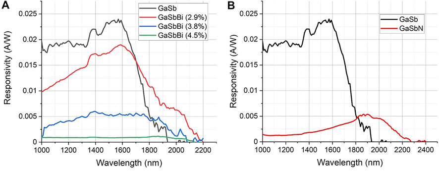
FIGURE 4. Spectral photo response of (A) GaSb and GaSbBi MSM-PDs and (B) GaSb and GaNSb MSM-PDs with different incorporation, measured at room temperature.
The comparison between measured GaSb and GaNSb devices shown in Figure 4B illustrates that the peak responsivity for the GaNSb device. This indicates that the peak responsivity for the GaSbN sample decreases to 5.39 × 10⁻³ A/W at 1900 nm. This appears to be a much faster decrease in the measured responsivity compared to the GaSbBi devices (where Bi content of up to around 3% could be added before significant degradation was observed). The reason for this is likely to be the greater strain introduced when incorporating N compared with Bi into GaSb, resulting in a greater density of defects.
The overall comparison of the responsivity and external quantum efficiency (calculated by comparing the responsivity with the theoretical maximum responsitivy achievable at the peak wavelength) is listed in Table. 3. The associated R0A values, as calculated from the IV data in Figure 1 and the peak specific detectivity (so called D*) value for each device are also compared in Table 3 All of the devices studied have relatively small R0A and D* values compared to other GaSb devices reported (Chen et al., 2018; Fang et al., 2018). However it should be noted that the objective of this work was not to obtain optimised performance (which often requires more exotic devices than reported here) but to observe the effects that incorporating Bi and N into these alloys had on performance. The value of D* is inversely proportional to the Noise Equivalent Power (NEP) of the detector and directly proportional to the responsivity, therefore by either increasing the responsivity or decreasing the noise the measured detectivity can be increased. It is likely that improved design, growth and fabrication can lead to significant increases for each of the devices. For example as already noted only around 25% of the incident light is absorbed in the epitixal layer limiting the responsivity. We have also previously shown (Cao et al., 2019) that post growth annealing can improve the material quality of similar GaSbBi layers by reducing the number of defects which will likely have a positive impact on the RoA and D* values. The choice of metal for Schotkky barrier and electrode geometry are also to be optimised. Given that GaSb detectors have been reported elsewhere with higher D* values than this work (Mansoor et al., 1995; Chen et al., 2018), it is encouraging that we can incorporate around 3% of Bi with almost no change in our value and only observe a decrease by a factor of about 20 at the highest Bi contents, while incorporating N only reduces the peak D* by a factor of about 5. These results are therefore encouraging that with improved design (i.e., resonant cavities, plasmonic absorber, etc.) in principle Bi and N can be incorporated into GaSb photodetectors and still maintain a good level of performance.
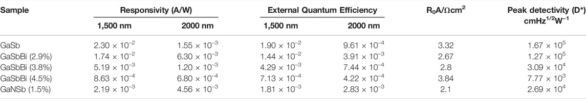
TABLE 3. Comparison of devices responsivity and external quantum efficiency at different wavelength.
The effect of different geometry on the spectral photo responses has also been compared between the bar and zigzag interdigital electrode geometries. For devices with the same electrode spacing no observable difference is measured between the straight and zigzag configurations. This indicates that the increased electrode perimeter from the interdigitated configuration has only a negligible effect on the final device responsivity. Previous studies on MSM-PDs have shown that the final device performance can be greatly influenced by the electrode spacing (Averine et al., 2001; Averine et al., 2008). In these it was shown that, as the electrode gap increased, the response time of the photodetector to an incident pulse increases due to the increased transit time.
Figure 5 shows the responsivity as a function of the electrode gap for each of the devices. All measurements are for devices with the straight bar electrode configuration. Multiple devices were tested for each, with Figure 4 showing the average values. While each shows a fall in the responsivity as the gap spacing is increased, as would be expected due to the increased transit time (Averine et al., 2001), the rate of decrease is much larger for the Bi and N containing samples, with the rate of decrease appearing to increase as more Bi is introduced. This indicates that there is an additional degradation in the transit time upon the addition of dilute amounts of Bi or N. A likely explanation of this phenomenon is the increase in the trap density for the Bi and N samples, with the resultant traps then restricting the extraction of photo generated carriers within the gap, effectively increasing the average transit time for the carriers (Segercrantz et al., 2017).
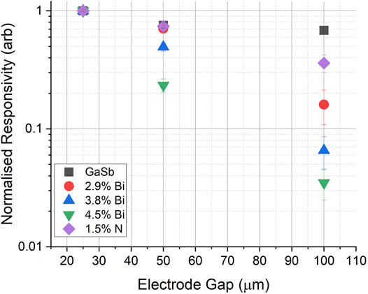
FIGURE 5. Normalised Peak Responsivity as a function of the electrode gap.
Conclusion
In this paper, the viability of incorporating Bi and N into GaSb layers and their use as MSM-PDs has been studied. The cut-off wavelength and photo spectral responses of MSM-PDs have been investigated. Clear wavelength extension has been observed for GaSbBi and GaNSb samples, with the cut-off wavelength extended to 1950 nm (2.9% Bi), 1990 nm (3.8% Bi), 2080 nm (4.5% Bi) and 2190 nm (1.5% N), demonstrating the viability of using Bi and N for mid-infrared sensing. The band-gap reduction for GaSbBi and GaNSb samples, obtained from wavelength extension, of 27 ± 3 meV/%Bi for GaSbBi and 103 meV/%N for GaSbN devices. Both of these are lower than those that have been previously reported, in the case of the GaSbBi samples, this seems to be due to the indirect GaSb valance band to GaSbBi conduction band transition dominating over the expected direct transition. For the GaNSb sample the reason is not clear although may be due to non-uniform N composition across the wafer. While we have not been able to directly measure the response time of the detectors in this work, analysis of the photoresponse when changing the distance between the electrodes indicates an increase in the response time as the Bi incorporation is increased. In terms of the other classic 5S parameters of a detector (Liao, 2021) we have demonstrated that Bi and N can be incorpotated into GaSb devices with only a modest decrease in the responsivity, and no significant change in the dark current, resulting in a slight reduction in the specific detectivity (conversely considered as an increase in the NEP) while increasing the spectral range of the detectors.
Data Availability Statement
The raw data supporting the conclusion of this article will be made available by the authors, without undue reservation.
Author Contributions
Epitaxial Samples were designed by TV and MA and grown by MA. Device design and fabrication undertaken by IS and ZC. Measurements performed by IS, ZC, and SH. Analysis of results undertaken by IS, ZC, TV, SH, and MA.
Conflict of Interest
The authors declare that the research was conducted in the absence of any commercial or financial relationships that could be construed as a potential conflict of interest.
Publisher’s Note
All claims expressed in this article are solely those of the authors and do not necessarily represent those of their affiliated organizations, or those of the publisher, the editors and the reviewers. Any product that may be evaluated in this article, or claim that may be made by its manufacturer, is not guaranteed or endorsed by the publisher.
References
Adachi, S. (1987). Model Dielectric Constants of Gap, Gaas, Gasb, Inp, Inas, and Insb. Phys. Rev. B 35 (14), 7454–7463. doi:10.1103/physrevb.35.7454
Adachi, S. (1989). Optical Dispersion Relations for GaP, GaAs, GaSb, InP, InAs, InSb, Al X Ga1− X as, and In1− X Ga X as Y P1− Y. J. Appl. Phys. 66 (12), 6030–6040. doi:10.1063/1.343580
Averine, S. V., Chan, Y. C., and Lam, Y. L. (2001). Geometry Optimization of Interdigitated Schottky-Barrier Metal–Semiconductor–Metal Photodiode Structures. Solid-State Electron. 45 (3), 441–446. doi:10.1016/s0038-1101(01)00017-x
Averine, S. V., Kuznetzov, P. I., Zhitov, V. A., and Alkeev, N. V. (2008). Solar-blind MSM-Photodetectors Based on AlxGa1− xN/GaN Heterostructures Grown by MOCVD. Solid-State Electron. 52 (5), 618–624. doi:10.1016/j.sse.2007.10.037
Buckle, L., Bennett, B. R., Jollands, S., Veal, T. D., Wilson, N. R., Murdin, B. N., et al. (2005). Growth of Dilute GaNSb by Plasma-Assisted MBE. J. Cryst. Growth 278 (1-4), 188–192. doi:10.1016/j.jcrysgro.2004.12.148
Cao, Z. M., Veal, T. D., Ashwin, M. J., Dawson, K., and Sandall, I. (2019). Influence of Annealing on the Electrical Characteristic of GaSbBi Schottky Diodes. J. Appl. Phys. 126 (5), 053103. doi:10.1063/1.5108870
Cao, Z., Ashwin, M., Veal, T., and Sandall, I. (2020). “GaSbBi Metal-Semiconductor-Metal Photodetectors for Mid-Infrared Sensing,” in IEEE Photonics Conference (IPC), September 7, 2020.
Chen, Y.-H., Jheng, J.-W., Mishra, P., Lin, C.-Y., and Lee, M.-C. M. (2018). GaSb MSM Photodetectors on Si Waveguides by Rapid Melt Growth Method. IEEE Phot. Technol. Lett. 30 (11), 1013–1015. doi:10.1109/lpt.2018.2805679
Das, S. K., Das, T. D., Dhar, S., De La Mare, M., and Krier, A. (2012). Near Infrared Photoluminescence Observed in Dilute GaSbBi Alloys Grown by Liquid Phase Epitaxy. Infrared Phys. Technol. 55 (1), 156–160. doi:10.1016/j.infrared.2011.11.003
Das, S., Bhowal, M. K., and Dhar, S. (2019). Calculation of the Band Structure, Carrier Effective Mass, and the Optical Absorption Properties of GaSbBi Alloys. J. Appl. Phys. 125 (7), 075705. doi:10.1063/1.5065573
Delorme, O., Cerutti, L., Luna, E., Narcy, G., Trampert, A., Tournié, E., et al. (2017). GaSbBi/GaSb Quantum Well Laser Diodes. Appl. Phys. Lett. 110 (22), 222106. doi:10.1063/1.4984799
Delorme, O., Cerutti, L., Tournié, E., and Rodriguez, J.-B. (2017). Molecular Beam Epitaxy and Characterization of High Bi Content GaSbBi Alloys. J. Cryst. Growth 477, 144–148. doi:10.1016/j.jcrysgro.2017.03.048
Fang, X., Wei, Z., Fang, D., Chu, X., Tang, J., Wang, D., et al. (2018). Surface State Passivation and Optical Properties Investigation of GaSb via Nitrogen Plasma Treatment. Acs Omega 3 (4), 4412–4417. doi:10.1021/acsomega.7b01783
Haas, J., and Mizaikoff, B. (2016). Advances in Mid-infrared Spectroscopy for Chemical Analysis. Annu. Rev. Anal. Chem. 9, 45–68. doi:10.1146/annurev-anchem-071015-041507
Jefferson, P. H., Veal, T. D., Piper, L. F. J., Bennett, B. R., McConville, C. F., Murdin, B. N., et al. (2006). Band Anticrossing in GaNxSb1-X. Appl. Phys. Lett. 89 (11), 111921. doi:10.1063/1.2349832
Jiang, J., Shterengas, L., Hosoda, T., Belyanin, A., Kipshidze, G., and Belenky, G. (2018). GaSb-Based Diode Lasers with Asymmetric Coupled Quantum Wells. Appl. Phys. Lett. 113 (7), 071106. doi:10.1063/1.5046426
Jurczak, P., Sablon, K. A., Gutiérrez, M., Liu, H., and Wu, J. (2017). 2.5-µm InGaAs Photodiodes Grown on GaAs Substrates by Interfacial Misfit Array Technique. Infrared Phys. Technol. 81, 320–324. doi:10.1016/j.infrared.2017.02.001
Karstad, K., Stefanov, A., Wegmuller, M., Zbinden, H., Gisin, N., Aellen, T., et al. (2005). Detection of Mid-IR Radiation by Sum Frequency Generation for Free Space Optical Communication. Opt. lasers Eng. 43 (3-5), 537–544. doi:10.1016/j.optlaseng.2004.05.006
Kopaczek, J., Kudrawiec, R., Linhart, W. M., Rajpalke, M. K., Yu, K. M., Jones, T. S., et al. (2013). Temperature Dependence of the Band Gap of GaSb1-xBix Alloys with 0 < X <= 0.042 Determined by Photoreflectance. Appl. Phys. Lett. 103 (26), 261907. doi:10.1063/1.4858967
Kopaczek, J., Kudrawiec, R., Linhart, W., Rajpalke, M., Jones, T., Ashwin, M., et al. (2014). Low- and High-Energy Photoluminescence from GaSb1-xBix with 0 < X <= 0.042. Appl. Phys. Express 7 (11), 111202-1–111202-6. doi:10.7567/apex.7.111202
Lei, W., Antoszewski, J., and Faraone, L. (2015). Progress, Challenges, and Opportunities for HgCdTe Infrared Materials and Detectors. Appl. Phys. Rev. 2 (4), 041303. doi:10.1063/1.4936577
Liao, M. (2021). Progress in Semiconductor Diamond Photodetectors and MEMS Sensors. Funct. Diam. 1 (1), 29–46. doi:10.1080/26941112.2021.1877019
Mansoor, F., Grey, R., and Haywood, S. K. (1995). Long-Wavelength Gaas/Alas Distributed Bragg Reflectors for Use in Gasb-Based Resonant-Cavity Detectors. Electron Lett. 31 (3), 200–202. doi:10.1049/el:19950113
Mudd, J. J., Kybert, N. J., Linhart, W. M., Buckle, L., Ashley, T., King, P. D. C., et al. (2013). Optical Absorption by Dilute GaNSb Alloys: Influence of N Pair States. Appl. Phys. Lett. 103 (4), 042110. doi:10.1063/1.4816519
Polak, M. P., Scharoch, P., Kudrawiec, R., Kopaczek, J., Winiarski, M. J., Linhart, W. M., et al. (2014). Theoretical and Experimental Studies of Electronic Band Structure for GaSb1− xBix in the Dilute Bi Regime. J. Phys. D. Appl. Phys. 47 (35), 355107. doi:10.1088/0022-3727/47/35/355107
Rajpalke, M. K., Linhart, W. M., Birkett, M., Yu, K. M., Scanlon, D. O., Buckeridge, J., et al. (2013). Growth and Properties of GaSbBi Alloys. Appl. Phys. Lett. 103 (14), 142106. doi:10.1063/1.4824077
Rajpalke, M. K., Linhart, W. M., Birkett, M., Yu, K. M., Alaria, J., Kopaczek, J., et al. (2014). High Bi Content GaSbBi Alloys. J. Appl. Phys. 116 (4), 043511. doi:10.1063/1.4891217
Rajpalke, M. K., Linhart, W. M., Yu, K. M., Jones, T. S., Ashwin, M. J., and Veal, T. D. (2015). Bi Flux-dependent MBE Growth of GaSbBi Alloys. J. Cryst. Growth 425, 241–244. doi:10.1016/j.jcrysgro.2015.02.093
Razeghi, M., and Nguyen, B.-M. (2014). Advances in Mid-infrared Detection and Imaging: a Key Issues Review. Rep. Prog. Phys. 77 (8), 082401. doi:10.1088/0034-4885/77/8/082401
Rothman, L. S., Gamache, R., Tipping, R., Rinsland, C., Smith, M., Benner, D. C., et al. (1992). The HITRAN Molecular Database: Editions of 1991 and 1992. J. Quant. Spectrosc. Radiat. Transf. 48 (5-6), 469–507. doi:10.1016/0022-4073(92)90115-k
Samajdar, D. P., Das, T. D., and Dhar, S. (2015). Valence Band Anticrossing Model for GaSb1− xBix and GaP1− xBix Using Kp Method. Mater. Sci. Semicond. Process. 40, 539–542. doi:10.1016/j.mssp.2015.06.065
Segercrantz, N., Makkonen, I., Slotte, J., Kujala, J., Veal, T. D., Ashwin, M. J., et al. (2015). Increased P-type Conductivity in GaN X Sb1− X, Experimental and Theoretical Aspects. J. Appl. Phys. 118 (8), 085708. doi:10.1063/1.4929751
Segercrantz, N., Slotte, J., Makkonen, I., Tuomisto, F., Sandall, I. C., Ashwin, M. J., et al. (2017). Hole Density and Acceptor-type Defects in MBE-Grown GaSb1-xBix. J. Phys. D. Appl. Phys. 50 (29), 1–6. doi:10.1088/1361-6463/aa779a
Sharma, A. S., and Dhar, S. (2019). Influence of Bi on the Temperature Dependent Fundamental Band Gap Parameters of GaSb1− xBix. Mat. Res. Express 6 (4), 046208. doi:10.1088/2053-1591/aafeee
Soibel, A., Wright, M. W., Farr, W. H., Keo, S. A., Hill, C. J., Yang, R. Q., et al. (2009). Midinfrared Interband Cascade Laser for Free Space Optical Communication. IEEE Photonics Technol. Lett. 22 (2), 121–123. doi:10.1109/LPT.2009.2036449
Veal, T. D., Piper, L. F. J., Jollands, S., Bennett, B. R., Jefferson, P. H., Thomas, P. A., et al. (2005). Band Gap Reduction in GaNSb Alloys Due to the Anion Mismatch. Appl. Phys. Lett. 87 (13), 132101. doi:10.1063/1.2058224
Vineis, C., Wang, C., Jensen, K., and Breiland, W. (1998). In Situ monitoring of GaSb, GaInAsSb, and AlGaAsSb. J. Cryst. growth 195 (1-4), 181–186. doi:10.1016/s0022-0248(98)00699-x
Wang, D., Svensson, S. P., Shterengas, L., Belenky, G., Kim, C. S., Vurgaftman, I., et al. (2009). Band Edge Optical Transitions in Dilute-Nitride GaNSb. J. Appl. Phys. 105 (1), 014904. doi:10.1063/1.3055273
Weiss, E., Klin, O., Benory, E., Kedar, E., and Juravel, Y. (2001). Substrate Quality Impact on the Carrier Concentration of Undoped Annealed HgCdTe LPE Layers. J. Electron. Mater. 30 (6), 756–761. doi:10.1007/bf02665868
Yang, R. Q. (2020). Electronic States and Interband Tunneling Conditions in Type-II Quantum Well Heterostructures. J. Appl. Phys. 127 (2), 025705. doi:10.1063/1.5133801
Keywords: Gasbbi, photodetector, bismuth, metal-semiconductor-metal, semiconductor III-V
Citation: Cao Z, Hulme S, Veal TD, Ashwin MJ and Sandall I (2022) GaSbBi Metal Semiconductor Metal Detectors for Mid-Infrared Sensing. Front. Electron. Mater. 2:895959. doi: 10.3389/femat.2022.895959
Received: 14 March 2022; Accepted: 30 May 2022;
Published: 16 June 2022.
Edited by:
Baolai Liang, University of California, Los Angeles, United StatesReviewed by:
Kausik Majumdar, Indian Institute of Science (IISc), IndiaMeiyong Liao, National Institute for Materials Science, Japan
Copyright © 2022 Cao, Hulme, Veal, Ashwin and Sandall. This is an open-access article distributed under the terms of the Creative Commons Attribution License (CC BY). The use, distribution or reproduction in other forums is permitted, provided the original author(s) and the copyright owner(s) are credited and that the original publication in this journal is cited, in accordance with accepted academic practice. No use, distribution or reproduction is permitted which does not comply with these terms.
*Correspondence: Ian Sandall, SXNhbmRhbGxAbGl2ZXJwb29sLmFjLnVr