 Leila Rahimifard1†
 Ahish Shylendra 1†
 Shamma Nasrin 1Stephanie E. Liu 2
 Vinod K. Sangwan 2Mark C. Hersam 2,3,4
 Amit Ranjan Trivedi1*
- 1Department of Electrical and Computer Engineering, University of Illinois at Chicago, Chicago, IL, United States
- 2Department of Materials Science and Engineering, Northwestern University, Evanston, IL, United States
- 3Department of Chemistry, Northwestern University, Evanston, IL, United States
- 4Department of Electrical and Computer Engineering, Northwestern University, Evanston, IL, United States
The increasing complexity of deep learning systems has pushed conventional computing technologies to their limits. While the memristor is one of the prevailing technologies for deep learning acceleration, it is only suited for classical learning layers where only two operands, namely weights and inputs, are processed simultaneously. Meanwhile, to improve the computational efficiency of deep learning for emerging applications, a variety of non-traditional layers requiring concurrent processing of many operands are becoming popular. For example, hypernetworks improve their predictive robustness by simultaneously processing weights and inputs against the application context. Two-electrode memristor grids cannot directly map emerging layers’ higher-order multiplicative neural interactions. Addressing this unmet need, we present crossbar processing using dual-gated memtransistors based on two-dimensional semiconductor MoS2. Unlike the memristor, the resistance states of memtransistors can be persistently programmed and can be actively controlled by multiple gate electrodes. Thus, the discussed memtransistor crossbar enables several advanced inference architectures beyond a conventional passive crossbar. For example, we show that sneak paths can be effectively suppressed in memtransistor crossbars, whereas they limit size scalability in a passive memristor crossbar. Similarly, exploiting gate terminals to suppress crossbar weights dynamically reduces biasing power by ∼20% in memtransistor crossbars for a fully connected layer of AlexNet. On emerging layers such as hypernetworks, collocating multiple operations within the same crossbar cells reduces operating power by
1 Introduction
The increasing complexity of deep neural networks (DNN) and their proliferating applications in embedded computing have pushed conventional architectures and CMOS technologies to their limits (Shukla et al., 2021b; Nasrin et al., 2021; Kim et al., 2020; Iliev et al., 2019). As a result, there is an invigorated interest in exploring alternative technologies and computing architectures to achieve a disruptive improvement in deploying DNNs under stringent area, power, and latency constraints. Memristors are among the most promising emerging non-volatile memory technologies for DNNs (Prezioso et al., 2015; Cheng et al., 2017; Li et al., 2018; Ankit et al., 2019; Wang et al., 2019). Memristors can store DNN’s synaptic weights in a dense and scalable crossbar architecture with multibit precision and passive resistive programming. Moreover, the same crossbar can be used for “compute-in-memory” processing of certain key computations of a DNN. Integrating storage and computations within the same structure allows memristor crossbars to supersede conventional digital accelerators where limited memory-processor bandwidth becomes the key bottleneck for performance scaling (Chen et al., 2016; Basu et al., 2018; Kim et al., 2020).
In parallel, DNN architectures are going through a dramatic evolution to improve their computational efficiency. In the last few years, novel layers such as inception (Szegedy et al., 2016), residual layers (Szegedy et al., 2017), dynamic gating (Hua et al., 2018), polynomial layers (Kileel et al., 2019), self-attention (Wu et al., 2019), and hypernetworks (Ha et al., 2016) have been added to the repository of DNN building blocks. Therefore, a critical challenge for the next generation of DNN accelerators is to exhibit high versatility in their processing flow for efficiently mapping these various DNN layers into hardware circuits. Emerging architectures use additional layers beyond the classical layers, and thus, they can simultaneously correlate multiple variables to enhance the computational efficiency and representation capacity. For example, hypernetworks (Ha et al., 2016) integrate the application context in their prediction by simultaneously correlating all three, viz., inputs, weights, and context features to predict the output. Likewise, recurrent layers such as gated recurrent units (GRU) simultaneously correlate input and weight dot products against history-dependent reset vector using Hadamard product for long or short-term memory.
While a significant advantage of memristor crossbars is their scalability via two-electrode arrays, this same architecture imposes challenges when adapting their use for such emerging DNN layers. Due to only two controlling electrodes, memristor crossbars are only suited for classical DNN layers where only two operands, namely weights and inputs, are processed at a given time. Memristor grids cannot directly map emerging DNN layers where multiple operands must be simultaneously processed. A two-electrode control of memristors also creates challenges for computational scalability. For example, mixed-signal operations on memristor crossbars are susceptible to sneak current paths formed dynamically depending on the input and weight vectors. To suppress these sneak paths, memristor cells in a crossbar are typically integrated with additional selector components such as transistors or diodes. Although the selectors improve the robustness of crossbar processing, the additional circuit elements per cell sacrifice the crossbar scalability and pose other constraints on materials compatibility during fabrication.
In this work, we present a neural network crossbar based on dual-gated memtransistors (Figure 1) to overcome the limitations of memristor crossbars for higher-order processing of emerging deep learning layers. Unlike memristors, memtransistors are multi-terminal gate-tunable active elements whose non-volatile resistance can be persistently programmed but volatile channel resistance can also be adapted dynamically by gate electrodes. The gate-tunability of memtransistors also offers unprecedented circuit and microarchitecture-level co-optimization opportunities for neural crossbars, especially for emerging deep learning layers that rely on higher-order multiplicative interactions.
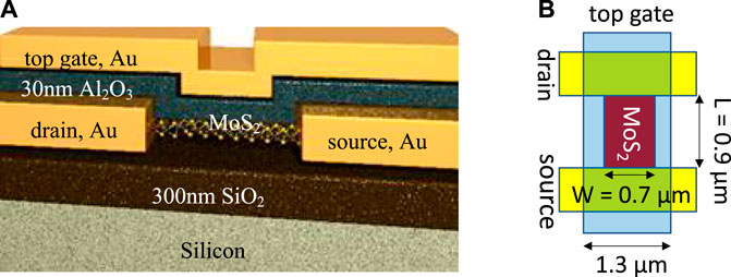
FIGURE 1. Dual-gated memtransistors: (A) Schematic of a dual-gated memtransistor on monolayer MoS2. (B) Top view schematic of a crossbar cell.
Exploiting the dual-gated MoS2 memtransistors for neural processing, our key contributions in this work on classical and emerging neural layers are as follows:
• Classical layers on memtransistor crossbars: We propose a higher-order neural network processing method using a dual-gated memtransistor crossbar in the time and charge domain. In our scheme, inputs are applied row-wise in the time domain, and outputs are accumulated column-wise in the charge domain. The proposed gate-tunable neural processing significantly enhances the scalability of the crossbar and minimizes overheads of mixed-signal processing and peripherals. For example, we exploit gate tunability of memtransistors to eliminate sneak current paths in the crossbar. When time-encoded input to a row is low, memtransistors in the respective row are configured to a very high resistance state using gate controls to suppress sneak current paths. In comparison, conventional memristor crossbars require additional selectors at each cell to control the sneak path and/or are limited to operating with a smaller crossbar size. In addition, by using the gate-tunability of memtransistors, conductance-emulated crossbar weights are dynamically suppressed based on input patterns such that the overall prediction accuracy is not affected but the crossbar’s overall biasing power can be minimized. Although similar input-adaptive weight suppression is also feasible in memristor crossbars, only hard weight gating can be implemented without significantly complicating the physical design. Meanwhile, gate-tunability of memtransistors naturally allows a soft-gating of network weights which opens many more excellent opportunities for crossbar weight adaptation without sacrificing accuracy.
• Emerging layers on memtransistor crossbars: We discuss mapping schemes for emerging higher-order neural layers on memtransistor crossbars, namely, hypernetworks and history-dependent gating mechanisms in long-short term memory (LSTM) and gated recurrent units (GRU). The implementations reveal the significant efficiency of memtransistor crossbars to implement the emerging layers than conventional memristor crossbars. Dual gate controls of memtransistor allow quadratic order multiplications to be implemented within a single device, reducing the total number of operations and processing modules. For example, for hypernetworks, quadratic multiplications within a memtransistor crossbar are
Section 2 discusses the background on fabrication and operating characteristics of memtransistors. Section 3 discusses the advantages of memtransistor crossbars on classical neural network layers. Section 4 presents the benefits of memtransistor crossbars for emerging neural network layers such as Hypernetworks and LSTM on the memtransistor grid. Finally, Section 5 summarizes our key advancements and concludes.
2 Gate-tunable dual-gated memtransistor crossbars
In prior works (Sangwan et al., 2018; Lee et al., 2020), our co-authors Sangwan and Hersam have demonstrated a novel gate-tunable memristive system—the memtransistor—fabricated from polycrystalline monolayer MoS2 with SiO2 as the bottom gate dielectric. For the individual dual-gated memtransistor (Figure 1A), the drain and source electrodes were patterned by electron beam lithography and liftoff processes on MoS2 that was synthesized by chemical vapor deposition. This is followed by patterning of MoS2 channels by reactive ion etching (channel length L and width W are 900 and 700 nm, respectively). The top-gate dielectric Al2O3 (30 nm thick) were grown by atomic layer deposition. A 300-nm-thick SiO2 acted as the gate dielectric on the doped Si wafer serving as a global bottom gate. The dual-gated memtransistor crossbar was fabricated using the same channel geometry, the thickness of metal electrodes, and the thickness of dielectrics layers as the individual devices. Figure 1B shows the channel dimensions of each node in the fabricated crossbar. Figure 1C shows the micrograph of a representative dual-gated 10-by-9 crossbar array. The source and drain terminal lines are interleaved, running in parallel, for a higher density of memtransistor cells. The top gate lines run orthogonal to source/drain terminals. Various other adaptations of memtransistors have been discussed in our prior works Yan X. et al., 2021; Yuan et al., 2021; Sangwan et al., 2015.
2.1 Operating principles of the dual-gated memtransistor
Figure 2A shows the characteristic pinched memristive loop and measured bipolar resistive switching characteristics of the dual-gated MoS2 memtransistor at different bottom gate biases VBG with a floating top gate. The device is initially in a low resistance state (LRS) and switches to a high resistance state (HRS) at forward bias (drain voltage VDS > 0), representing a RESET process. In contrast, the device undergoes a SET process (i.e., switching from HRS to LRS) at reverse bias (VDS < 0). The clockwise switching in SET/RESET processes and inverted rectification polarity suggest that the bottleneck for charge injection occurs at the drain electrode. Thus the dominant resistive switching mechanism occurs at the forward-biased Schottky diode (i.e., under the drain contact in RESET, source contact in SET). This is in contrast to the dominant resistive switching mechanism in reverse-biased Schottky diode at source contacts in single-gated memtransistors (Sangwan et al., 2018, 2015), as shown in Figure 2B. The possible physical mechanisms for the different behavior are discussed in detail in the Lee et al. (2020). The reversible and dynamic modulation of the Schottky barrier could be attributed to the migration of defects or charge trapping events near the contacts in the underlying MoS2 or overlaying Al2O3. Most importantly, the dual-gated memtransistor (Lee et al., 2020) enables not only gate-tunable learning, like the single-gated memtransistor (Sangwan et al., 2018), but also permits efficient scaling into a crossbar array configuration by suppression of sneak currents, unlike the single-gated memtransistor. Memtransistor-based spiking neuron implementations were discussed in prior works Yuan et al., 2021; Yan et al., 2021b whereas this paper focuses on higher order deep learning using the devices.
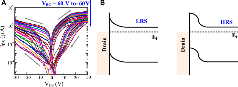
FIGURE 2. Memtransistor characteristics and mechanism: (A) Drain current (IDS) versus drain bias (VDS) characteristics of a dual-gated MoS2 memtransistor. Gate tunable memristive switching is seen at various bottom gate biases (VBG) while the top gate is floating. (B) Left: Schematic diagram showing a Schottky contact and MoS2 band-bending near the drain electrode in low resistance state (LRS). EF is the Fermi energy level. Right: Schematic diagram showing the increased space-charge region near the drain electrode in high resistance state (HRS). Reproduced with permission (Sangwan et al., 2018). Copyright 2018, The Authors, published by Springer Nature.
2.2 Modelling of single gate memtransistor characteristics
In Sangwan et al., 2018, we have discussed memtransistor modeling under a single gate adaptation of the device. A brief summary is provided here. We model the memtransistor behavior by integrating a mathematical formalism of memristive systems with the charge transport model of a Schottky-barrier FET (SB-FET). Memristive systems are defined as:
where t is the time, w is an internal state variable, and V and I are the input (voltage) and output (current). In the sub-threshold regime, the charge transport in SB-FET is dominated by thermionic emission:
where A∗ is the 2D equivalent Richardson constant, the term T3/2 comes from the 2D model (as opposed to T2 in 3D), Φb is the barrier height. Combining SB-FET model with memristive formalism, we derive:
Here, A, D, E, cr, cvd, p, and Δn are fitting parameters. We omit greater details of the above equation here for brevity that can be referred in our prior work Sangwan et al., 2018.
2.3 Projection of dual-gated memtransistor to scaled dimensions
Dimensions of our prototype memtransistors are not scaled to achieve practical low power advantages for neural processing. While our device scaling efforts are underway (Lee et al., 2020), in this work, we project dual-gated memtransistor nodes to approach tens of nanometers and study the potential benefits of crossbar-based neural processing using simulations. In the fabricated prototypes, non-volatility of resistance states is experimentally verified to originate from Schottky Barrier (SB) height modulation. Therefore, to study the device characteristics at the nanometer scale, we integrate the formalism of non-equilibrium Green function (NEGF)-based current conduction and SB height modulation. A NEGF-based model can preserve the wave (quantum-mechanical) character of carrier electrons at the scaled dimensions, and therefore, it is more accurate than classical current transport equations.
Figure 3A shows the schematic of a dual-gated memtransistor with a channel length of 7 nm for simulation using NEGF. The scaled device in the figure is used for our ensuing discussions. The channel in the device is formed using monolayer MoS2. Top gate is patterned on 2 nm thick Al2O3 dielectric. In the fabricated prototype, see Figure 1, MoS2 is grown on SiO2 and a doped silicon layer is used as a bottom gate. Appropriately, a bottom (or back) gate under 10 nm thick SiO2 is considered in the scaled adaptation. Under various SB height (ΔϕB) programming, Figure 3B shows ID-VGS characteristics of the scaled device at VDS = 0.3 V and Figure 3C shows ID-VDS characteristics at the top gate potential being 0.5 V. Due to thermionic emission-based current conduction, IDS through a memtransistor is exponentially sensitive to gate voltage VGS. At varying programming configurations, IDS changes by one to three-orders of magnitude by switching gate voltage to zero from 0.5 V. Therefore, to suppress sneak paths, memtransistor crossbars can utilize gate-tunability of IDS; the advantages of these characteristics will be analyzed in more details subsequently.
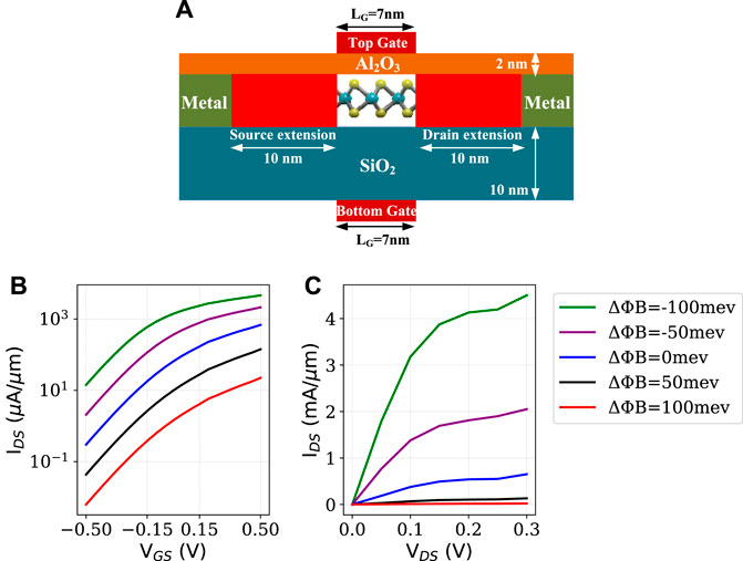
FIGURE 3. Memtransistor characteristics simulations: (A) Scaled dimensions of memtransistor evaluated under NEGF. (B) IDS-VGS at varying Schottky Barrier height (VDS = 0.3 V). The potential at the top gate is sweeping while the potential at the bottom gate is set to 0 V. (C) IDS–VDS at varying SB height. The potential at the top gate is 0.5 V and at the back gate is zero.
2.4 Comparison to competitive synaptic memory technologies
Table 1 compares the proposed technology against the competitive synaptic memory technologies for neural crossbars. Characteristics and benchmarks of other technologies are gathered from Chen 2016; Choi et al., 2020; Cai et al., 2017; Yu and Chen 2016; Endoh et al., 2016; Mladenov 2019, 2020; Mladenov and Kirilov 2013. Two key advantages of memtransistors are multi-terminal control, thus eliminating the need for dedicated selector devices, and potential for better crossbar density due to superlative gate electrostatics even at sub-10 nm scaling. In the demonstrated prototypes Sangwan et al., 2018; Lee et al., 2020; Sangwan and Hersam 2020; Sangwan et al., 2017; Yan X. et al., 2021, HRS/LRS ratio, retention, and endurance are already comparable to the best-reported characteristics among nonvolatile memories (NVMs). Although our current prototype has a larger dimension, at sub-10 nm channel lengths, write voltage is expected to be less than 2 V with latency less than 10 nanoseconds.
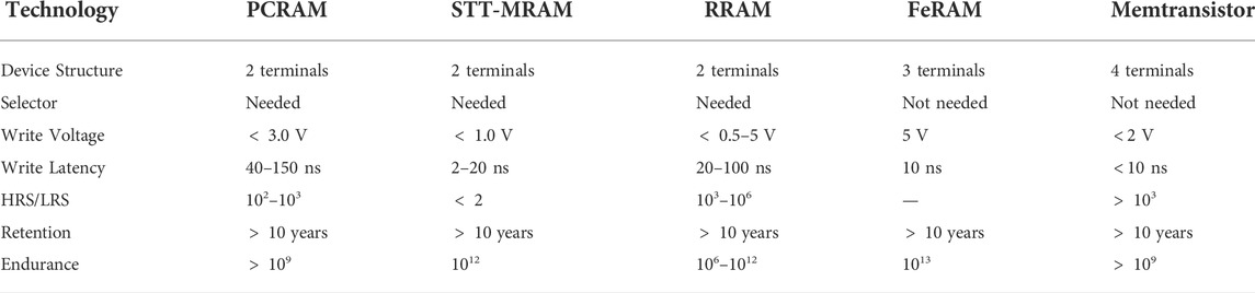
TABLE 1. Comparison of device-level characteristics of memtransistor against conventional NVMs.
Furthermore, memtransistors have critical advantages over dual gate synaptic transistors such as in Yan M. et al., 2021; Tian et al., 2019. In memtransistors, the non-volatile resistive switching is achieved by the drain bias pulses. Therefore, one of the gate terminal can afford the tunability of the resistive states to realize multi-state memory or change the learning rate during neural network training. Importantly, this can be achieved without the second gate that can be then used as a selector to suppress the sneak current in the scaled network. So, the second gate acts as a transistor in a 1T1M architecture of memristor crossbars while the second gate can control learning behavior. On other hand, dual-gated synaptic transistors Yan M. et al., 2021; Tian et al., 2019 achieve non-volatile memory states using pulses on one of the gates, not by the drain electrode. So, the second gate can be used to either change the learning rate or act as a selector, but not for both simultaneously. Therefore, dual-gated memtransistors allow an additional control electrode that is not feasible in dual-gated synaptic transistors. These differences have also been outlined in detailed comparison between different dual-gated synaptic devices including ferroelectric devices in the review article Yan X. et al., 2021.
3 Classical neural layers on memtransistor crossbars
This section studies the advantages of dual-gated memtransistor crossbars for classical deep learning layers. We first discuss a time/charge-domain neural processing scheme simplifies crossbar processing peripherals. Subsequently, we discuss how dual-gate control of memtransitor crossbars can be exploited to dynamically suppress sneak paths and layer weights to maximize the energy efficiency of neural processing.
3.1 Crossbar architecture and time-domain processing
Figure 4 shows the architecture of a crossbar where each cell is made of a dual-gated memtransistor. The drains electrodes of memtransistors along a row are shared and controlled together. The source electrodes of memtransistors along a column are also shared. Dual-gate grids are formed within a crossbar. Front gates of memtransistors along a row are shared, creating a row-wise front-gate grid. Back-gates along a column are shared, forming a column-wise back-gate grid. Comparable memtransistor crossbars were fabricated in Feng et al., 2021. A weight matrix is mapped on a memtransistor grid by programming the height of each crossbar element’s Schottky barrier (SB). An input vector is applied row-wise on the drain ends of memtransistors in the time-domain using digital to pulse converter DAC (T-DAC). T-DAC is composed of digital components—a digital comparator and register to store crossbar inputs—where the count from a digital counter is compared against the stored input. An active high signal is inserted if the count is less than the input.
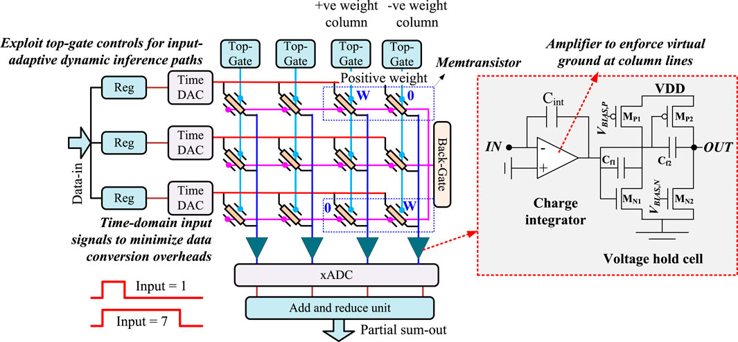
FIGURE 4. Time-domain processing in memtransistor crossbars: Inputs are applied in the time-domain. Inputs and weights are multiplied in the charge domain. Integrator and hold circuit for charge accumulation are shown on the right.
Subsequently, the crossbar operates on time-encoded input signals against the stored weights. Each memtransistor is programmed so that its conductance (gij) at the applied time-encoded input pulse between its drain to source electrodes is proportional to the mapped weight magnitude wij. Since the conductance of a memtransistor can only be positive, whereas the weight matrix values can be both positive and negative, two crossbar cells—positive and negative weight cells—are dedicated for each weight matrix entry, as shown in the figure. The figure shows that positive or negative weight matrix entries are written on the corresponding cell while the other cell is programmed to the minimum conductance.
When input pulses are applied, each memtransistor injects a current Iij = IDS(ϕij) along a column as long as the pulse is active. Here, ϕij is the programmed Schottky barrier height of a memtransistor at the iij row and jij column, programmed according to the corresponding weight value wij mapped at the intersection. Along a column, columns currents are integrated on a capacitor CINT using a charge integrator circuit shown to the right side of Figure 4. At the end of crossbar processing, the potential developed across the integrating capacitor follows ∑Ti × Iij/CINT. Here, Ti is the pulse-width of the encoded input vector element at row “i” and Iij is the current of memtransistor at the iij row and jij column. The front-end amplifier in the charge integrator enforces a virtual ground on the sources of memtransistors to improve the reliability of current integration.
An integrated charge can be held briefly using a voltage hold cell shown to the right in the figure. Hold-cell is designed using common-source (CS) amplifiers with both NMOS (MN1) and PMOS (MP2) input stage to accommodate for rail-to-rail swing of the integrator output and feedback capacitors (Cf1 and Cf2). The potential at the charge-integrator output degrades over time due to crossbar’s leakage. Such degradation will alter the biasing of MN1 and MP2, causing the output of the CS stage to increase due to negative feedback and resulting in potential differences across feedback capacitors. The resulting current through the feedback capacitors due to the potential difference restores charge-integrator output and thereby enhances the retention time of the hold-cell.
The complexity of time-domain digital to analog converter (T-DAC) and voltage-domain analog to digital converter (ADC) in Figure 4 increases exponentially with higher precision input and output processing. Memtransistors can only support a limited precision weight storage. Therefore, the operating precision of neural crossbar is inherently limited. Higher precision inputs and weights can be bit-sliced to alleviate precision scalability challenges, as shown in Figure 4. For example, 8-bit input and weight values can be time-sliced into four-bit sections and four operation cycles can be used for processing. Although the crossbar’s latency increases, its design and implementation become significantly simplified. Similar memristor and other non-volatile memory-based neural accelerators have also been studied in prior works (Trivedi and Mukhopadhyay 2014; Manasi and Trivedi 2016; Shafiee et al., 2016; Wang et al., 2016; Mikhailenko et al., 2018; Nasrin et al., 2019; Fernando et al., 2020; Ma et al., 2020; Nasrin et al., 2020; Shukla et al., 2021a). However, our subsequent discussion will highlight how dual-gated control of the memtransistor grid can offer unique co-optimization opportunities not available to current memristor-based crossbar designs.
3.2 Crossbar scalability with gate-controlled sneak path suppression
A critical challenge for conventional crossbar scaling is the presence of sneak current paths. Consider the earlier discussed time-domain neural processing in a crossbar in Figure 5A. As a vector of time-domain inputs is applied along the rows, charge domain processing in the array computes input vector-weight matrix products along with columns in voltage mode, which must be digitized for downward processing and transmission. Since a typical analog-to-digital converter (ADC) requires significant area/power overhead, integrating parallel ADCs at each crossbar column incurs excessive overhead. Thus typically, only a limited number of integrated ADCs will multiplex over all crossbar columns to sequentially digitize their output. Under such ADC multiplexing, the analog output of a column held at the charge integrator is susceptible to degradation under charge leakage. Therefore, to minimize the crossbar’s bias power under ADC’s multiplexing, only a limited number of column outputs (such as 16 in a crossbar with 128 columns) are computed in one-time step, and the remaining crossbar columns are left floating to prevent leakage power. However, floating crossbar columns can form sneak paths affecting the output accuracy, whereas the number of such sneak paths dramatically increases with increasing crossbar size.
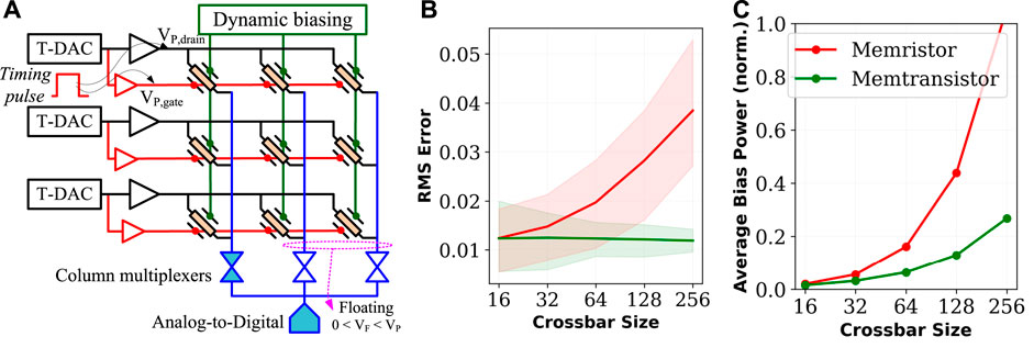
FIGURE 5. Sneak current path analysis of memtransistor crossbar: (A) Sneak paths in a crossbar can arise due to practical considerations such as column multiplexing with limited number of ADCs which requires unselected (floating) columns. For memristor and memtransistor crossbars: (B) average and worse-case scalar product error at increasing crossbar size, and (C) average biasing power if unselected crossbar columns are grounded in memristor crossbars.
In a memtransistor crossbar, gate-bias of crossbar elements can be employed to suppress such sneak paths dynamically. Figure 5A shows the proposed scheme where timing pulses from T-DAC are applied to both drain and gate of a memtransistor. As T-DAC pulses deactivate, the gate voltage of memtransistors along the row is swept from 0 V to −0.5 V, which increases their resistance by orders of magnitude (see Figure 3B) and effectively suppresses the sneak paths formed through floating memtransistor columns. Although similar implementation can be used for memristor crossbars by integrating a transistor in each crossbar cell (Zidan et al., 2014; Yan et al., 2016; Humood et al., 2019; Shi et al., 2020), memtransistors achieve this in a single circuit device.
Figure 5B shows the root-mean-square (RMS) error for memristor-based crossbar arrays against memtransistor crossbar arrays where gate voltages are exploited to suppress sneak current paths dynamically. Various simulation parameters are listed in Table 2. Memtransistors with W/L = 10 nm/7 nm are used for each crossbar cell where ϕB programming within ∼150 mV window varies drain-to-source current Ids from 1–100 nA at drain VD. When the input from T-DAC deactivates, VD of memtransistors along the row is grounded and VG is biased at −0.5 V to cut-off sneak paths as discussed before. An equivalent resistance programming range is assumed for memristors to highlight the advantages of gate tunability in memtransistors specifically. Timing DACs are operated with 4-bit precision and take a minimum time-step of 0.2 ns. 6-Bit precision ADCs are integrated with a crossbar and one ADC operation consumes 8.3 fJ based on the energy model in Ginsburg 2007. Simulations were performed using SPICE. The simulation results show average and worst-case performance over hundred simulations on random input and weight vectors. The error distribution is shown in shaded red and green colors for memristor and memtransistor crossbars.
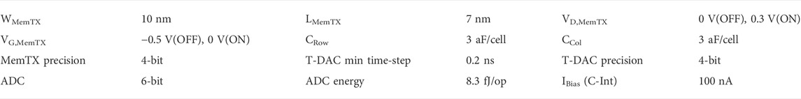
TABLE 2. Memtransistor (MemTX) crossbar simulation parameters.
Note that the sneak current paths problem deteriorates in memristor crossbars with increasing crossbar size, causing degradation to the output, thereby limiting the size of the largest crossbar that can be reliably processed. In the proposed memtransistor crossbar operation, we can control sneak current to the instrumentation noise floor since each gate is connected to the input. Thus, the error is almost independent of the size of the array and is only impacted by the non-idealities of peripherals such as limited OP-AMP gain (∼100 in our case). Moreover, the average power consumption can be significantly reduced in the dual-gated memtransistor crossbar, as shown in Figure 5C. If such sneak paths were to be suppressed by grounding unselected columns in the memristor crossbar, the resulting waste in biasing power would invariably scale with crossbar size as shown in Figure 5C. In avoiding the requirement to ground unselected crossbar columns, memtransistor crossbars can achieve much better energy efficiencies than memristor crossbars.
3.3 Input adaptive deep learning with dynamic weights
The input-adaptive inference is becoming prominent in improving the energy efficiency of deep learning. The central idea in input-adaptive inference is to dynamically re-adjust input-output connections in each layer based on the input characteristics and complexity. For example, complex input patterns can be processed with a more sophisticated inference model, i.e., more weights and more levels of abstractions (DNN layers). In contrast, simpler inputs can be operated with a low complexity model with fewer weights yet maintaining high prediction accuracy. For such input adaptive deep learning, Liu et al. Liu and Deng 2018 discussed dynamic deep neural networks (D2NN) where input-output connections in each deep learning layer are dynamically dropped based on the input characteristics. Channel gating neural networks were discussed in Hua et al. (2019) where channels that contribute less to the classification result are identified and skipped dynamically. Dynamic slimmable networks were presented in Li et al., 2021 exploring a better mapping efficiency under such dynamic pruning by keeping filters stored statically and contiguously in memories.
However, most input-adaptive inference techniques applicable for memristor crossbars show significant training complexity related to the lack of dynamic tunability of the memristor’s characteristics. Since that resistance of a memristor can not be modulated in runtime, only hard gating of output neurons can be implemented. Under such hard gating, an output neuron is completely dropped (gated) depending on the input pattern and thereby its associated bias power on synaptic connections can be saved. However, hard gating of neurons requires adding discrete optimization steps in the learning procedure. Thereby, computationally expensive discrete optimization methods (such as REINFORCE Cai et al., 2018) or reinforcement learning Liu and Deng 2018 are necessitated which significantly increases the training workload. While hard gating of DNN neurons is essential for memristor grids, by exploiting their gate tunability, memtransistor grids can utilize soft gating of neurons for enhanced opportunities for input-adaptive bias power saving as well as simplified learning procedures. Under soft gating, an output neuron can dynamically scale down its synaptic strength through gate tunability of the memtransistor grid. Since the bias power for a weight-input product at an output neuron is proportional to the total conductance of associated synapses, the associated bias power can be saved by scaling down its synaptic weights. We discuss how dual-gate control of memtransistor crossbars can efficiently implement such input-adaptive crossbar weight modulation. More importantly, we will discuss how dual-gate management simplifies the input-adaptive inference training procedure.
In Figure 6B, consider input-adaptation neurons Ai,1 to Ai,N interleaved with output neurons in a crossbar mapping layer i of a neural network. For input-adaptive crossbar energy minimization, the scheme follows a “soft-suppression” of output neurons by controlling their column-wise back gate voltages based on the output from the adaptation neurons. If an adaptation neuron suppresses an output neuron, its output voltage is low, reducing all weights in the output neuron’s column. We consider a block-wise input adaptation where neuron Aij regulates column-wise gate voltages of all output neurons in the respective block Bij as shown in the figure. The input-adaptation transpires in two phases. In the first phase, the output neuron’s suppression voltage are computed through adaptation neurons while disabling regular output neurons using column-wise gate voltages, i.e., VBG = 0 V. Adaptation neurons Aij in the layer perform scalar dot product of adaptation weight matrix and layer input yi−1 to compute the adaptation voltages of the corresponding block. In the second phase, layer outputs are computed by applying suppression voltages to the gate grid of output neurons, as shown in the figure. Thereby, weight matrix Wi of layer i is adapted to
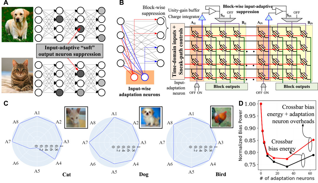
FIGURE 6. Dynamic inference paths: (A) Input-adaptive “soft” suppression of neurons. (B) Within crossbar computations of input-adaptive suppression factor. Input to a layer are applied to adaptation neurons which compute the suppression factor for primary neurons in the layer. Using the crossbar architecture shown to the right, the suppression factor is applied using vertical gate grid. (C) On CIFAR10 dataset, input-adaptive neural weight suppression factors computed for the fully-connected layer of AlexNet. (D) Bias-power saving with increasing number of adaptation neurons on fully-connected layer of AlexNet.
Notably, due to soft suppression of weights, the network is fully differentiable, thereby doesn’t introduce training complexities compared to typical DNNs. In Figure 6C, we consider a fully-connected layer of size 4,096 × 4,096 from AlexNet, trained with the CIFAR10 dataset, and apply the above input-adaptive inference with soft gating of neural weights. Weights of adaptation neurons Aij were trained by modifying the original weight matrix Wi to
4 Higher-order neural networks on memtransistor crossbars
Several new DNN layer styles are being developed to improve computational efficiency and to capture multiple inductive biases in deep learning. A noticeable trend among emerging DNN layer styles is that they exploit higher-order interaction among operands. For example, for inputs x, weight matrix W, and activation function f (), a classical first-order DNN layer computes f (Wx). Comparatively, a second-order DNN layer in hypernetworks computes
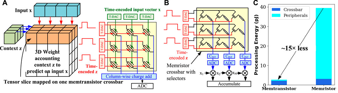
FIGURE 7. Hypernetworks on memtransistor crossbar: (A) Implementation of Hypernetworks on memtransistor crossbar and comparison to memristor crossbar-based mapping in (B). Context vector z is applied row-wise as pulse-width modulated signal and input vector x is applied column-wise. Charge integrated by all output columns is merged and passed to ADC for digitization. Compared to a memristor crossbar, the number of computing operations are minimized significantly. (C) Comparison of crossbar and peripheral energy between memristor and memtransistor crossbars for 64-by-64 weight matrix.
In a hypernetwork Ha et al., 2016, a neural network g generates weights of another network f given some context z. Hypernetworks have found critical success over traditional DNNs for generative modeling, continuous learning, and neural machine translation Klocek et al., 2019; Ehret et al., 2020; Spurek et al., 2020; Suarez 2017. Prior work Jayakumar et al., 2019 has shown that processing in hypernetworks is, in fact, equivalent to higher-order processing of input x and context z through a 3D weight tensor
Figure 7B shows a comparative mapping of hypernetworks on the memristor crossbar to illustrate the advantages of the memtransistor grid on such higher-order processing. Since memristors can only perform first-order matrix-vector multiplication, hypernetwork computations must be split into multiple steps in Figure 7B. Therefore, first, weight-slice Wi is processed against time-encoded context vector z using a memristor crossbar. Then, column outputs are digitized and multiplied digitally with input vector x. Finally, the product sum bits are digitally accumulated. For an n × m × k-sized 3D weight tensor
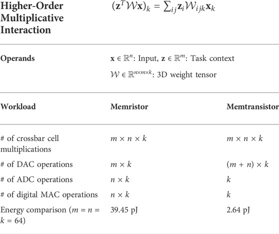
TABLE 3. Memtransistor vs. Memtransitors on Hypernetworks.
Considering a specific test-case of
In gated recurrent neural networks (RNN), such as long short term memory (LSTM) Hochreiter and Schmidhuber 1997 and gated recurrent units (GRU) Ravanelli et al., 2018, the role of previous output state ht−1 to current predictions ht is gated based on the predictions from a forget network rt using Hadamard product, i. e, ht−1 ⊙rt. Figure 8A shows such gating through coupled memtransistor crossbars. Here, the first crossbar Xbar1 computes the gating factors rt. Xbar2 is a special purpose crossbar where both gate lines run row-wise parallel. Significantly, by directly coupling Xbar1 and Xbar2, digital conversion of gating factors from Xbar1 to Xbar2 is not needed, and gating factors can be applied in the voltage domain itself. The activation layer, such as sigmoid on gating factors, can be implemented using an operational transconductance amplifier (OTA). Conversely, additional digital multiplications and domain conversions will be necessary if gating is mapped through the memristor crossbar. Due to such integrated processing, in Table 4 on a 64 × 64 random LSTM/GRU matrix operated on random inputs, memtransistors consume on average
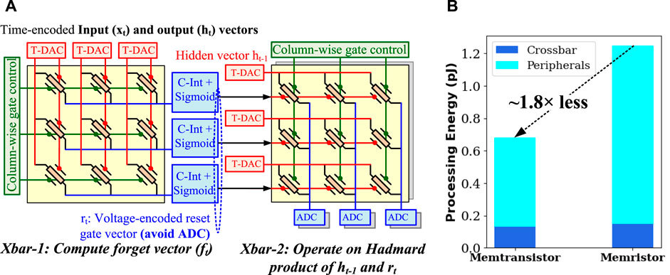
FIGURE 8. Other higher-order emerging layers on memtransistor crossbar: (A) Implementation of Hadamard product layers of LSTM and GRU using coupled memtransistor crossbars. Outputs from left crossbar are directly applied to the gate grid of right crossbar, and thereby the overhead of intermediate digitization is saved. (B) Energy comparisons between memristor and memtransistor-based implementation of Hadamard gating mechanisms.
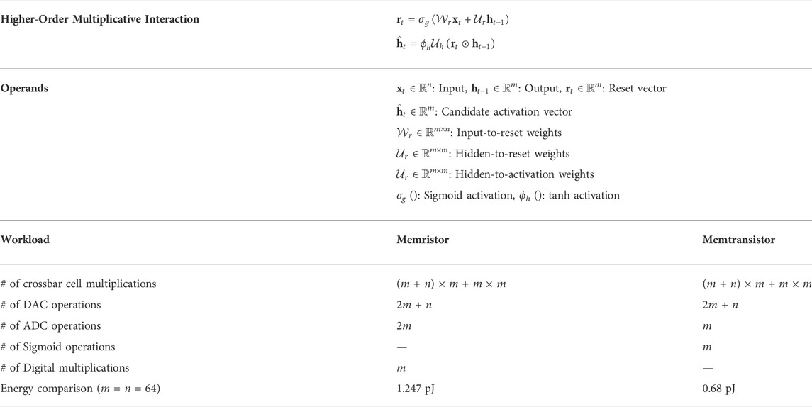
TABLE 4. Memtransistor vs. Memtransitors on Gated Recurrent Units.
Likewise, attention mechanisms can be efficiently implemented on memtransistor crossbars. In particular, recent work has shown remarkably simpler neural architectures composed entirely of attention mechanisms Vaswani et al., 2017. An attention function can be described as mapping a query and a set of key-value pairs to an output. For a multi-headed attention in Vaswani et al. (2017), each attention layer i computes
5 Conclusion
We have discussed emerging trends in deep learning where recent higher-order neural network layers and input adaptive deep learning rely on higher-order multiplicative interactions. Since memristors are two-terminal passive devices, they cannot efficiently emulate such higher-order computations and cannot take advantage of the ongoing algorithmic innovations. Overcoming this critical gap between hardware technologies and emerging neural network layer architectures, we have discussed neural processing with dual-gated memtransistor crossbars. Due to dual-gate controls, memtransistor crossbars can be dynamically adapted by suppressing sneak paths or adapting against input characteristics. Furthermore, dual-gate tunability of memtransistors allows mapping higher-order computations on a single crossbar cell, which results in a significant reduction of analog-to-digital conversions and crossbar biasing power.
Data availability statement
The original contributions presented in the study are included in the article/supplementary material, further inquiries can be directed to the corresponding author.
Author contributions
AT, VS, and MH developed the ideas. LR and SL developed device-level studies. AS and SN performed application-level simulations.
Funding
This work was primarily supported by National Science Foundation (NSF) Grant Number CCF-2106964.
Conflict of interest
The authors declare that the research was conducted in the absence of any commercial or financial relationships that could be construed as a potential conflict of interest.
Publisher’s note
All claims expressed in this article are solely those of the authors and do not necessarily represent those of their affiliated organizations, or those of the publisher, the editors and the reviewers. Any product that may be evaluated in this article, or claim that may be made by its manufacturer, is not guaranteed or endorsed by the publisher.
References
Ankit, A., Hajj, I. E., Chalamalasetti, S. R., Ndu, G., Foltin, M., Williams, R. S., et al. (2019). “Puma: A programmable ultra-efficient memristor-based accelerator for machine learning inference,” in Proceedings of the twenty-fourth international conference on architectural support for programming languages and operating systems, 715–731.
Basu, S., Bryant, R. E., De Micheli, G., Theis, T., and Whitman, L. (2018). Nonsilicon, non-von neumann computing—Part i [scanning the issue]. Proc. IEEE 107, 11–18. doi:10.1109/jproc.2018.2884780
Bellet, A., Habrard, A., and Sebban, M. (2015). Metric learning. Synthesis Lect. Artif. Intell. Mach. Learn. 9, 1–151. doi:10.2200/s00626ed1v01y201501aim030
Cai, H., Kang, W., Wang, Y., Naviner, L. A. D. B., Yang, J., Zhao, W., et al. (2017). High performance mram with spin-transfer-torque and voltage-controlled magnetic anisotropy effects. Appl. Sci. 7, 929. doi:10.3390/app7090929
Cai, H., Zhu, L., and Han, S. (2018). Proxylessnas: Direct neural architecture search on target task and hardware. arXiv preprint arXiv:1812.00332.
Chen, A. (2016). A review of emerging non-volatile memory (nvm) technologies and applications. Solid-State Electron. 125, 25–38. doi:10.1016/j.sse.2016.07.006
Chen, Y.-H., Emer, J., and Sze, V. (2016). Eyeriss: A spatial architecture for energy-efficient dataflow for convolutional neural networks. SIGARCH Comput. Archit. News 44, 367–379. doi:10.1145/3007787.3001177
Cheng, M., Xia, L., Zhu, Z., Cai, Y., Xie, Y., Wang, Y., et al. (2017). Time: A training-in-memory architecture for memristor-based deep neural networks. In 2017 54th ACM/EDAC/IEEE design automation conference (IEEE), 1–6.
Choi, H.-S., Park, Y. J., Lee, J.-H., and Kim, Y. (2020). 3-d synapse array architecture based on charge-trap flash memory for neuromorphic application. Electronics 9, 57. doi:10.3390/electronics9010057
Ehret, B., Henning, C., Cervera, M. R., Meulemans, A., von Oswald, J., and Grewe, B. F. (2020). Continual learning in recurrent neural networks with hypernetworks. arXiv preprint arXiv:2006.12109.
Endoh, T., Koike, H., Ikeda, S., Hanyu, T., and Ohno, H. (2016). An overview of nonvolatile emerging memories—Spintronics for working memories. IEEE J. Emerg. Sel. Top. Circuits Syst. 6, 109–119. doi:10.1109/jetcas.2016.2547704
Feng, X., Li, S., Wong, S. L., Tong, S., Chen, L., Zhang, P., et al. (2021). Self-selective multi-terminal memtransistor crossbar array for in-memory computing. ACS Nano 15, 1764–1774. doi:10.1021/acsnano.0c09441
Fernando, B. R., Qi, Y., Yakopcic, C., and Taha, T. M. (2020). “3d memristor crossbar architecture for a multicore neuromorphic system,” in 2020 international joint conference on neural networks (IEEE), 1–8.
Ginsburg, B. P. (2007). Energy-efficient analog-to-digital conversion for ultra-wideband radio. Cambridge, MA: Ph.D. thesis, Massachusetts Institute of Technology.
Hochreiter, S., and Schmidhuber, J. (1997). Long short-term memory. Neural Comput. 9, 1735–1780. doi:10.1162/neco.1997.9.8.1735
Hua, W., Zhou, Y., De Sa, C. M., Zhang, Z., and Suh, G. E. (2019). “Channel gating neural networks,” in Advances in neural information processing systems. 1886–1896.
Hua, W., Zhou, Y., De Sa, C., Zhang, Z., and Suh, G. E. (2018). Channel gating neural networks. arXiv preprint arXiv:1805.12549.
Humood, K., Hadi, S. A., Mohammad, B., Abi Jaoude, M., Alazzam, A., and Alhawari, M. (2019). “High-density reram crossbar with selector device for sneak path reduction,” in 2019 31st international conference on microelectronics (IEEE), 244–248.
Iliev, N., Gianelli, A., and Trivedi, A. R. (2019). Low power speaker identification by integrated clustering and Gaussian mixture model scoring. IEEE Embed. Syst. Lett. 12, 9–12. doi:10.1109/les.2019.2915953
Jayakumar, S. M., Czarnecki, W. M., Menick, J., Schwarz, J., Rae, J., Osindero, S., et al. (2019). “Multiplicative interactions and where to find them,” in International conference on learning representations.
Kileel, J., Trager, M., and Bruna, J. (2019). On the expressive power of deep polynomial neural networks. Adv. Neural Inf. Process. Syst. 32, 10310–10319.
Kim, B., Lee, S., Trivedi, A. R., and Song, W. J. (2020). Energy-efficient acceleration of deep neural networks on realtime-constrained embedded edge devices. IEEE Access 8, 216259–216270. doi:10.1109/access.2020.3038908
Klocek, S., Maziarka, Ł., Wołczyk, M., Tabor, J., Nowak, J., and Śmieja, M. (2019). “Hypernetwork functional image representation,” in International conference on artificial neural networks (Springer), 496–510.
Lee, H.-S., Sangwan, V. K., Rojas, W. A. G., Bergeron, H., Jeong, H. Y., Yuan, J., et al. (2020). Dual-gated MoS2 memtransistor crossbar array. Adv. Funct. Mat. 30, 2003683. doi:10.1002/adfm.202003683
Li, C., Belkin, D., Li, Y., Yan, P., Hu, M., Ge, N., et al. (2018). Efficient and self-adaptive in-situ learning in multilayer memristor neural networks. Nat. Commun. 9, 2385. doi:10.1038/s41467-018-04484-2
Li, C., Wang, G., Wang, B., Liang, X., Li, Z., and Chang, X. (2021). “Dynamic slimmable network,” in Proceedings of the IEEE/CVF conference on computer vision and pattern recognition, 8607–8617.
Liu, L., and Deng, J. (2018). Proceedings of the AAAI Conference on Artificial Intelligence, 32.Dynamic deep neural networks: Optimizing accuracy-efficiency trade-offs by selective execution.
Ma, X., Yuan, G., Lin, S., Ding, C., Yu, F., Liu, T., et al. (2020). “Tiny but accurate: A pruned, quantized and optimized memristor crossbar framework for ultra efficient dnn implementation,” in 2020 25th asia and south pacific design automation conference (IEEE), 301–306.
Manasi, S. D., and Trivedi, A. R. (2016). Gate/source-overlapped heterojunction tunnel fet-based lamstar neural network and its application to eeg signal classification. In Int. Jt. Conf. Neural Netw. (IEEE), 955–962.
Mikhailenko, D., Liyanagedera, C., James, A. P., and Roy, K. (2018). “M 2 ca: Modular memristive crossbar arrays,” in 2018 IEEE international symposium on circuits and systems (ISCAS) (IEEE), 1–5.
Mladenov, V. (2020). “A modified tantalum oxide memristor model for neural networks with memristor-based synapses,” in 2020 9th international conference on modern circuits and systems technologies (IEEE), 1–4.
Mladenov, V. (2019). Analysis of memory matrices with hfo2 memristors in a pspice environment. Electronics 8, 383. doi:10.3390/electronics8040383
Mladenov, V., and Kirilov, S. (2013). “Analysis of the mutual inductive and capacitive connections and tolerances of memristors parameters of a memristor memory matrix,” in 2013 European conference on circuit theory and design (IEEE), 1–4.
Nasrin, S., Drobitch, J. L., Bandyopadhyay, S., and Trivedi, A. R. (2019). Low power restricted Boltzmann machine using mixed-mode magneto-tunneling junctions. IEEE Electron Device Lett. 40, 345–348. doi:10.1109/led.2018.2889881
Nasrin, S., Drobitch, J., Shukla, P., Tulabandhula, T., Bandyopadhyay, S., Trivedi, A. R., et al. (2020). Bayesian reasoning machine on a magneto-tunneling junction network. Nanotechnology 31, 484001. doi:10.1088/1361-6528/abae97
Nasrin, S., Shukla, P., Jaisimha, S., and Trivedi, A. R. (2021). “Compute-in-memory upside down: A learning operator co-design perspective for scalability,” in 2021 design, automation & test in europe conference & exhibition (DATE) (IEEE), 890–895.
Prezioso, M., Merrikh-Bayat, F., Hoskins, B., Adam, G. C., Likharev, K. K., Strukov, D. B., et al. (2015). Training and operation of an integrated neuromorphic network based on metal-oxide memristors. Nature 521, 61–64. doi:10.1038/nature14441
Ravanelli, M., Brakel, P., Omologo, M., and Bengio, Y. (2018). Light gated recurrent units for speech recognition. IEEE Trans. Emerg. Top. Comput. Intell. 2, 92–102. doi:10.1109/tetci.2017.2762739
Sangwan, V. K., and Hersam, M. C. (2020). Neuromorphic nanoelectronic materials. Nat. Nanotechnol. 1–12, 517–528. doi:10.1038/s41565-020-0647-z
Sangwan, V. K., Jariwala, D., Kim, I. S., Chen, K.-S., Marks, T. J., Lauhon, L. J., et al. (2015). Gate-tunable memristive phenomena mediated by grain boundaries in single-layer MoS2. Nat. Nanotechnol. 10, 403–406. doi:10.1038/nnano.2015.56
Sangwan, V. K., Lee, H.-S., Bergeron, H., Balla, I., Beck, M. E., Chen, K.-S., et al. (2018). Multi-terminal memtransistors from polycrystalline monolayer molybdenum disulfide. Nature 554, 500–504. doi:10.1038/nature25747
Sangwan, V. K., Lee, H.-S., and Hersam, M. C. (2017). “Gate-tunable memristors from monolayer MoS2,” in 2017 IEEE international electron devices meeting (IEEE), 5–1.
Shafiee, A., Nag, A., Muralimanohar, N., Balasubramonian, R., Strachan, J. P., Hu, M., et al. (2016). Isaac: A convolutional neural network accelerator with in-situ analog arithmetic in crossbars. SIGARCH Comput. Archit. News 44, 14–26. doi:10.1145/3007787.3001139
Shi, L., Zheng, G., Tian, B., Dkhil, B., and Duan, C. (2020). Research progress on solutions to the sneak path issue in memristor crossbar arrays. Nanoscale Adv. 2, 1811–1827. doi:10.1039/d0na00100g
Shukla, P., Muralidhar, A., Iliev, N., Tulabandhula, T., Fuller, S. B., and Trivedi, A. R. (2021a). “Ultralow-power localization of insect-scale drones: Interplay of probabilistic filtering and compute-in-memory,” in IEEE transactions on very large scale integration (VLSI) systems.
Shukla, P., Nasrin, S., Darabi, N., Gomes, W., and Trivedi, A. R. (2021b). Mc-cim: Compute-in-memory with monte-carlo dropouts for bayesian edge intelligence. arXiv preprint arXiv:2111.07125.
Spurek, P., Winczowski, S., Tabor, J., Zamorski, M., Zieba, M., and Trzciński, T. (2020). Hypernetwork approach to generating point clouds. arXiv preprint arXiv:2003.00802.
Suarez, J. (2017). “Language modeling with recurrent highway hypernetworks,” in Advances in neural information processing systems, 3267–3276.
Szegedy, C., Ioffe, S., Vanhoucke, V., and Alemi, A. A. (2017). “Inception-v4, inception-resnet and the impact of residual connections on learning,” in Thirty-first AAAI conference on artificial intelligence.
Szegedy, C., Vanhoucke, V., Ioffe, S., Shlens, J., and Wojna, Z. (2016). “Rethinking the inception architecture for computer vision,” in Proceedings of the IEEE conference on computer vision and pattern recognition, 2818–2826.
Tian, B., Liu, L., Yan, M., Wang, J., Zhao, Q., Zhong, N., et al. (2019). Ferroelectric synapses: A robust artificial synapse based on organic ferroelectric polymer (adv. Electron. Mater. 1/2019). Adv. Electron. Mat. 5, 1970006. doi:10.1002/aelm.201970006
Trivedi, A. R., and Mukhopadhyay, S. (2014). Potential of ultralow-power cellular neural image processing with si/ge tunnel fet. IEEE Trans. Nanotechnol. 13, 627–629. doi:10.1109/tnano.2014.2318046
Vaswani, A., Shazeer, N., Parmar, N., Uszkoreit, J., Jones, L., Gomez, A. N., et al. (2017). Attention is all you need. Adv. neural Inf. Process. Syst. 30.
Wang, Y., Xia, L., Cheng, M., Tang, T., Li, B., and Yang, H. (2016). Proceedings of the International Conference on Compilers, Architectures and Synthesis for Embedded Systems, 1–2.Rram based learning acceleration.
Wang, Z., Li, C., Song, W., Rao, M., Belkin, D., Li, Y., et al. (2019). Reinforcement learning with analogue memristor arrays. Nat. Electron. 2, 115–124. doi:10.1038/s41928-019-0221-6
Wu, Y., Ma, Y., Liu, J., Du, J., and Xing, L. (2019). Self-attention convolutional neural network for improved mr image reconstruction. Inf. Sci. 490, 317–328. doi:10.1016/j.ins.2019.03.080
Yan, B., Mahmoud, A. M., Yang, J. J., Wu, Q., Chen, Y., and Li, H. H. (2016). “A neuromorphic asic design using one-selector-one-memristor crossbar,” in 2016 IEEE international symposium on circuits and systems (IEEE), 1390–1393.
Yan, M., Zhu, Q., Wang, S., Ren, Y., Feng, G., Liu, L., et al. (2021a). Ferroelectric synaptic transistor network for associative memory. Adv. Electron. Mat. 7, 2001276. doi:10.1002/aelm.202001276
Yan, X., Qian, J. H., Sangwan, V. K., and Hersam, M. C. (2021b). Progress and challenges for memtransistors in neuromorphic circuits and systems. Adv. Mat., 2108025. doi:10.1002/adma.202108025
Yu, S., and Chen, P.-Y. (2016). Emerging memory technologies: Recent trends and prospects. IEEE Solid-State Circuits Mag. 8, 43–56. doi:10.1109/mssc.2016.2546199
Yuan, J., Liu, S. E., Shylendra, A., Gaviria Rojas, W. A., Guo, S., Bergeron, H., et al. (2021). Reconfigurable MoS2 memtransistors for continuous learning in spiking neural networks. Nano Lett. 21, 6432–6440. doi:10.1021/acs.nanolett.1c00982
Keywords: memtransistor, crossbar, higher-order neural networks, input adaptive deep learning, hypernetworks, LSTM, attention, MoS2
Citation: Rahimifard L, Shylendra A, Nasrin S, Liu SE, Sangwan VK, Hersam MC and Trivedi AR (2022) Higher order neural processing with input-adaptive dynamic weights on MoS2 memtransistor crossbars. Front. Electron. Mater. 2:950487. doi: 10.3389/femat.2022.950487
Received: 22 May 2022; Accepted: 04 July 2022;
Published: 08 August 2022.
Edited by:
Nan Du, Chemnitz University of Technology, GermanyReviewed by:
Valeri Mladenov, Sofia Technical University, BulgariaBobo Tian, East China Normal University, China
Copyright © 2022 Rahimifard, Shylendra , Nasrin , Liu , Sangwan , Hersam and Trivedi. This is an open-access article distributed under the terms of the Creative Commons Attribution License (CC BY). The use, distribution or reproduction in other forums is permitted, provided the original author(s) and the copyright owner(s) are credited and that the original publication in this journal is cited, in accordance with accepted academic practice. No use, distribution or reproduction is permitted which does not comply with these terms.
*Correspondence: Amit Ranjan Trivedi, YW1pdHJ0QHVpYy5lZHU=
†These authors have contributed equal to this work